Aluminium Nanowires: Influence of Work Hardening on Conductance Histograms
Abstract
Conductance histograms of work-hardened Al show a series up to 11 equidistant peaks with a period of 1.150.02 of the quantum conductance unit . Assuming the peaks originate from atomic discreteness, this agrees with the value of 1.16 per atom obtained in numerical calculations by Hasmy et al..
pacs:
73.40.Jn, 61.46.+w, 68.65.LaStability and self-organization phenomena in metallic nanowires (NW) are controlled by an intimate combination of the quantum nature of the conduction electrons and the atomic-scale surface energy (for a review see Ref. Rev, ). At the scale of single atoms Au, Pt, and Ir spontaneously form into chains.Ohn ; AYan1 ; Smi For larger diameters more complex morphologies including spiral and helical multi-shell structures (often referred to as ‘weird wires’) were predicted Gul ; Tosatti and eventually observed in high-resolution transmission electron microscopy (TEM).Kon ; Osh ; Osh1
Electronic shell effects can stabilize and therefore favor certain geometries. Independent series of stable nanowire diameters with periodicities proportional to the square root of the conductance, , were observed for the free-electron-like alkali metals AYan2 ; AYan3 and the noble metals.Med ; Mar ; Mar1 Although these NWs were not imaged as by TEM, their stability was deduced from the statistical analysis of frequently occurring stable conductance values during breaking of the contacts.
With increasing NW diameter the contribution of the surface energy becomes more important and stable configurations are governed by the atomic packing. This gives rise to an atomic shell filling series and the crossover between electronic and atomic shell structure has been observed in the conductance of alkali and noble metals nanowires Mar ; Mar1 ; AYan4 as a change in the regular period on the scale . Atomic shell filling has been observed in TEM as exceptionally long and stable wires,Kon1 ; Kiz ; Rod predominantly along .
During last two years the effects of pseudoelastic deformation and shape memory in nanowires of the simple fcc metals (Ag, Cu) has drawn considerable attention.park ; liang These effects occur through the formation of defect-free twins during the to reorientation process. One can expect the emerging of stable configurations during a cycle of contraction and elongation of the NW. However, such configurations will be nanowire-specific and depend on NW diameter, crystallographic orientation, existence of defects etc. An example of striking repetitiveness of the conductance during the cyclical deformation (without breaking) of a long Au neck at 4.2 K was presented already in Ref. unt, .
Recently, we have reported the observation of a new series of structures periodic in , rather than , in conductance histograms of work hardened gold.Yan We suggested that heavy work hardening of the starting wire results in a high density of inter-crystalline boundaries and leads to texture of the most dense crystal planes [111], [100] and [110] being perpendicular to the nanowire axis. The distances between the maxima in conductance histograms correspond to the changes in the smallest cross section of densest planes by an integer number of atoms. The increment in conductance is then expected to scale as // 0.87/1/1.41 based on the size of the atomic unit cells. The Fourier transform of the data revealed three ‘frequencies’ at a close ratio: , 1.1, and . The mechanical properties of nanocrystalline materials (including NWs bietsch ) differ drastically from those of single crystals. In case of work hardened materials the mobility of atoms at grain boundaries may be high enough to adjust the local orientation of the grains on each side of the contact along one of the principal crystallographic axis.
Numerical simulations of conductance histograms for gold using a parameterized tight-binding approach were performed by Dreher et al.Dre They demonstrated for the main crystallographic orientations a series of peaks in histograms for the minimal cross sections that is related to the atomic discreteness. However they found this periodic structure in the minimal cross section was not reflected in conductance histograms in their calculations.
Here we report the observation of atomic-size oscillations for aluminium nanocontacts. The extension of this effect, previously observed for noble metals, to trivalent Al is of principal significance. One may anticipate that changing the nanowire cross section by a single atom for noble metals results in a change in conductance by approximately one quantum.Sch In Al three valence electrons give rise to three quantum channels: a highly transmissive channel with character and two low transmissive channels with a character.Cuevas ; Agr ; Sch1 The most unexpected result of our experiments is that the incremental conductance between adjacent maxima in conductance histograms of work-hardened Al is again close to one quantum conductance for up to about 11 oscillations (see below). In case of Al we can no longer apply quasi-classical considerations as we did for Au, and have to use a quantum mechanical approach. Such approach was elaborated by Hasmy et al.,Has1 ; Has2 who performed an embedded atom molecular dynamics method coupled with full quantum calculations of electron transport using a procedure based on the ab initio Gaussian embedded-cluster method.Pal The results reveal a statistically linear relationship between the conductance and the number of aluminium atoms in the contact cross-section with the slope equal to 1.16 .
Conductance histograms are constructed from a large number of contact-breaking traces and show the probability for observing a given conductance value . While for chemically inert gold conductance histograms of reasonable quality can be measured in air using very simple table-top devicesHansen this is much less obvious for chemically active aluminium, although some results have recently been reported.ancuta The main problem is that the hardness of aluminium oxide exceeds by far that of Al (9 versus 2.75 at Mohs scale of minerals hardness or 400 compared to 8 at absolute hardness scale ). The direct electrical contact between the electrodes can be established only by a ‘hard indenting’ procedure Sakai causing substantial damage to the lattice. An obvious solution to this problem is employing the mechanically controllable break junction (MCBJ) technique, described in details in Ref. Rev, . In our experiments the notched aluminium wire is broken under cryogenic vacuum conditions at 4.2 K exposing two electrodes with atomically clean surfaces. Accurately controlled indentation-retraction cycles can be obtained through the action of a piezoelectric element. On rare occasions () featureless or ill-reproducible histograms were observed with a small number of maxima positioned at significantly lower as compare to the rest of the data. Possibly this is caused by the break of the work hardened wire occurring along an oxidized microcrack or grain boundary.
For well-annealedanneal Al one typically observes several peaks in the histogram near , with (Fig. 1). One more peak is sometimes found near 5, but in most cases only peaks up to 3 are visible. Although a contribution of conductance quantization effects cannot be excluded completely, the main reason of the appearance of the peaks is the discreteness of the atomic structure of the contacts.Rev ; AYan5 The first peak results from single-atom contacts and higher peaks are due to stable atomic arrangements involving more atoms in the contact cross section (see Fig. 3 in Ref. Has2, ).
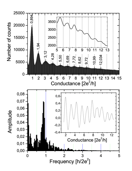
In our experiments we used two types of Al wires. Part of the measurements was done with commercial ‘temper hard’ samples.Adv Practically the same results were obtained by work hardening of annealed wires. To this end we pulled wires through a series of sapphire dies, reducing the diameter from 250 to 100m. In both cases it was possible to observe a structure periodic in having up to 11 oscillations in the conductance range from 0 to 13 (Fig. 2, upper panel). The position of maxima in the conductance histograms and their relative intensity were accurately reproduced for different samples.
The oscillating part of the histogram is presented in the inset to the lower panel of Fig. 2. It was obtained by subtracting the nearly linear background and by normalizing through division by the enveloping curve. The Fourier spectrum of this re-scaled histogram shows a peak at the ‘frequency’ 0.87 (lower panel in Fig. 2). Assuming the oscillations result from atomic discreteness in analogy to those observedYan for Au, this number is very close to the slope 0.86 obtained in numerical simulations for nanowires with a oriented axis.Has2
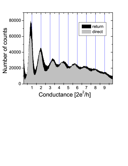
The histogram presented above was obtained for conductance traces recorded while breaking the contact. One can also take histograms for traces of contact-closing, which we refer to as return histograms. We measured direct and return histograms for work-hardened Al by applying an isosceles triangle ramp voltage to the piezodriver and separating data for the pulling and pushing part of the cycle. Surprisingly these histograms are practically equivalent (Fig. 3). This is quite different from our observations for work-hardened gold, where the number of the atomic-scale oscillations was greatly reduced in the return histograms and the electronic shell structure was observed in 40% of the latter.Yan
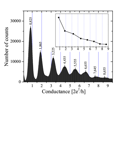
Conductance histograms for work-hardened Au invariably show a clear ‘beating’ pattern in the peak intensities related to the existence of several closely separated periodicities. In contrast for Al histograms with the largest number of peaks (10–11) we observed only a smooth decrease of the enveloping curve and a single frequency in the Fourier spectra around 0.87. In search for different periods we paid attention to histograms with lower numbers of peaks (Fig. 4). One notices kinks in the envelope curve for the histogram maxima (inset in Fig. 4). Although these irregularities may indicate contributions from the various axis orientations, the magnitude of the effect is rather small and the number of peaks in the histogram is not sufficient for more detailed analysis.
Assuming the periodicity being due to atom-size oscillation effects similar to our previous results on Au wiresYan we can estimate a Fermi wave vector in Al for effective free electrons propagating along (111) plane per one atom change of (111) cross section. Using the Sharvin formula, we obtain a value of m-1 for the effective momentum in Al.
The picture emerging from our experiments on Au Yan and more specifically for Al is as follows. For single crystalline necks with the highest atomic packing in the transverse crystal plane (like the (111) plane) not only are the Al atoms stacked at definite positions in the nodes of the lattice but their orbitals are also oriented in the same way. Hence three valence electrons contribute to the conductance with a contribution that scales with the number of atoms. This property is at the heart of the observed linear dependencies of contact conductance on the numbers of atoms in the smallest cross section of the nanowire. These atomic arrangements are associated with transient minima of the lattice free energy leading to maxima on conductance histograms.
Summarizing, we observed a new periodic structure in the conductance histograms of work hardened Al wires, which agrees with a series of stable wire cross sections given by integer numbers of atoms, combined with a conductance per atom as calculated by Hasmy et al.Has2 for the (111) orientation of nanowire axis. The experimentally observed peak in the Fourier transform at 0.87 is very close to the calculated value 0.86. We believe that this periodic structure is due to the same mechanism suggested for Au atomic-scale oscillations observed earlier.Yan
Part of this work was supported by Nanotechnology network in the Netherlands NanoNed, the Dutch nanotechnology programme of the Ministry of Economic Affairs, the Stichting voor Fundamenteel Onderzoek der Materie (FOM) which is financially supported by the Netherlands Organization for Scientific research (NWO), and the NANO-programm of Ukraine. O.I.S. wishes to acknowledge the FOM for a visitor’s grant.
References
- (1) N. Agraït, A. Levy Yeyati, and J. M. van Ruitenbeek, Phys. Rep. 377, 81 (2003).
- (2) H. Ohnishi, Y. Kondo, and K. Takayanagi, Nature (London) 395, 780 (1998).
- (3) A. I. Yanson, G. Rubio Bollinger, H. E. van den Brom, N. Agraït, and J. M. van Ruitenbeek, Nature (London) 395, 783 (1998).
- (4) R. H. M. Smit, C. Untiedt, A. I. Yanson, and J. M. van Ruitenbeek, Phys. Rev. Lett. 87, 266102 (2001).
- (5) O. Gulseren, F. Ercolessi, and E. Tosatti, Phys. Rev. Lett. 80, 3775 (1998).
- (6) E. Tosatti and S. Prestipino, Science, 289, 561 (2000).
- (7) Y. Kondo and K. Takayanagi, Science 289, 606 (2000).
- (8) Y. Oshima, H. Koizumi, K. Mouri, H. Hirayama, K. Takayanagi, and Y. Kondo, Phys. Rev. B 65, 121401 (2002).
- (9) Y. Oshima, A. Onga, and K. Takayanagi, Phys. Rev. Lett. 91, 205503 (2003).
- (10) A. I. Yanson, I. K. Yanson, and J. M. van Ruitenbeek, Nature (London) 400, 144 (1999).
- (11) A. I. Yanson, I. K. Yanson, and J. M. van Ruitenbeek, Phys. Rev. Lett. 84, 5832 (2000).
- (12) E. Medina, M. Diaz, N. Leon, C. Guerrero, A. Hasmy, P. A. Serena, and J. L. Costa-Kramer, Phys. Rev. Lett. 91, 026802 (2003).
- (13) A. I. Mares, A. F. Otte, L. G. Soukiassian, R. H. M. Smit, and J. M. van Ruitenbeek, Phys. Rev. B 70, 073401 (2004).
- (14) A. I. Mares and J. M. van Ruitenbeek, Phys. Rev. B 72, 205402 (2005).
- (15) Y. Kondo and K. Takayanagi, Phys. Rev. Lett. 79, 3455 (1997).
- (16) T. Kizuka, Phys. Rev. Lett. 81, 4448 (1998).
- (17) V. Rodrigues, T. Fuhrer, and D. Ugarte, Phys. Rev. Lett. 85, 4124 (2000).
- (18) H.S. Park, K. Gall, and J.A. Zimmerman, Phys.Rev.Lett. 95, 255504 (2005).
- (19) W. Liang and M. Zhou, Phys.Rev.B 73, 115409 (2006).
- (20) C. Untiedt, G. Rubio, S. Vieira, and N. Agraït, Phys. Rev. B 56, 2154 (1997).
- (21) A. I. Yanson, I. K. Yanson, and J. M. van Ruitenbeek, Phys. Rev. Lett. 87, 216805 (2001).
- (22) I. K. Yanson, O. I. Shklyarevskii, Sz. Csonka, H. van Kempen, S. Speller, A. I. Yanson, and J. M. Van Ruitenbeek, Phys. Rev. Lett. 95, 256806 (2005).
- (23) A. Bietsch and B. Michel, Appl. Phys. Lett. 80 3346 (2002).
- (24) M. Dreher, F. Pauly, J. Heurich, J. C. Cuevas, E. Scheer, and P. Nielaba, Phys. Rev. B 72, 075435 (2005).
- (25) E. Scheer, W. Belzig, Y. Naveh, M.H. Devoret, D. Esteve, and C. Urbina, Phys. Rev. Lett. 86, 284 (2001).
- (26) J. C. Cuevas, A. Levy Yeyati, and A. Martín-Rodero, Phys. Rev. Lett. 80, 1066 (1998).
- (27) J. C. Cuevas, A. Levy Yeyati, A. Martín-Rodero, G. Rubio Bollinger, C. Untiedt, and N. Agraït, Phys. Rev. Lett. 81, 2990 (1998).
- (28) E. Scheer, P. Joyez, D. Esteve, C. Urbina, and M.H. Devoret, Phys. Rev. Lett., 78, 3535 (1997).
- (29) A. Hasmy, E. Medina, and P. A. Serena, Phys. Rev. Lett. 86, 5574 (2001).
- (30) A. Hasmy, A. J. Perez-Jimenez, J. J. Palacios, P. Garcia-Mochales, J. L. Costa-Kramer, M. Diaz, E. Medina, and P. A. Serena, Phys. Rev. B 72, 245405 (2005).
- (31) J.J. Palacios, A.J. Perez-Jimenez, E. Louis, E. SanFabian, and J.A. Verges, Phys. Rev. B66, 035322 (2002).
- (32) K. Hansen, E. Lægsgaard, I. Stensgaard, and F. Besenbacher, Phys. Rev. B56, 2208 (1997).
- (33) A.I. Mares, D.F. Urban, J. Bürki, H. Grabert, C.A. Stafford, and J.M. van Ruitenbeek, cond-mat/0703589, Nanotechnology, in print.
- (34) J. Mizobata, A. Fujii, S. Kurokawa, and A. Sakai, Phys. Rev. B68, 155428 (2003)
- (35) A.I. Yanson and J.M. van Ruitenbeek, Phys. Rev. Lett. 79, 2157 (1997).
- (36) We used aluminium wire 125 diameter, “temper as drawn”, 99.99%+ , Goodfellow Corp. annealed in high vacuum at 350 C for 72 hours.
- (37) Aluminium wire, 125 diameter, “temper hard”, 99.99%, Advent Research Materials Ltd., Catalogue No. AL500111