Observation of a uniform temperature dependence in the electrical resistance across the structural phase transition in thin film vanadium oxide ()
Abstract
An electrical study of thin films in the vicinity of the structural phase transition at shows (a) that the electrical resistance follows over the -range, covering both sides of the structural transition, and (b) a history dependent hysteresis loop in upon thermal cycling. These features are attributed here to transport through a granular network.
pacs:
73.40.-c,73.43.Qt, 73.43.-f, 73.21.-bThe phase of the transition-metal-oxide vanadium-oxide undergoes a structural monoclinic- to tetragonal- phase transition in the vicinity of , which brings with it a band-realignment and an insulator-to-metal transition including, in high quality single crystals, orders-of-magnitude changes in the electrical resistance, and a dramatic alteration in the infrared optical transmission.1 ; 2 ; 3 ; 4 ; 5 ; 6 This interesting electronic-phase-transition has been attributed both to the Peierls-type period doubling lattice distortion, and an electron interaction induced Mott transition.2 ; 3 ; 4 ; 5 From a practical perspective, these large changes in the electrical and optical properties near room temperature have suggested as a smart material in future electro-optic applications. Studies have already shown that a large applied electrical bias7 ; 8 or intense photoexcitation9 ; 10 ; 11 ; 12 can trigger the electrical transition even below the structural transition temperature. Indeed, the electrical transition can be very fast, , in thin films and small particles.10 ; 11 ; 12 This confluence of practical and scientific interest have motivated investigations that aim to better understand the basics, and simultaneously obtain control over the insulator-metal transition, independent of the structural transition.
Here, we characterize and study thin films, which have thus far generally exhibited less dramatic changes than single crystals over the above mentioned transition(s). Thus, thin films of were deposited by electron beam evaporation of pellets, onto photolithographically patterned rectangular windows ranging from 200 x 400 down to 50 x 12.5 , on R-plane sapphire substrates.13 The film thickness was 350 nm. After liftoff, Cr/Au was thermally evaporated onto contact-pad-windows in the photoresist, and this was followed by metal liftoff. The contact fabrication was completed by a slow thermal anneal at . The reported vs. and the measurements were carried in a two-terminal configuration. Typically, the resistance was collected during both the up sweep and the down sweep of . measurements were carried out concurrently at a series of fixed , with the bias ramped in both directions; these results were insensitive to the bias sweep direction.
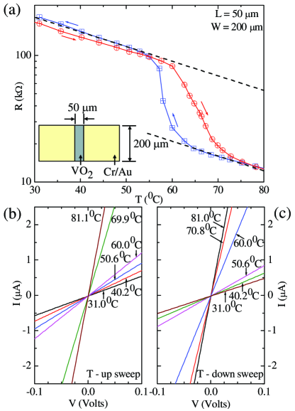
Figure 1(a) shows the resistance, , of a long wide film. This trace shows the electrical switching from a monoclinic, high resistance, nominally ”insulating” state to a tetragonal, lower resistance, nominally ”metallic” state, and the switching occurs occurs at a higher temperature on the up sweep- than on the down sweep- of .1 Other notable features observed in Fig. 1(a) are (i) a difference in the base temperature resistance at the outset- and at the end- of the measurement, (ii) an approximate linear decrease of the resistance with increasing on the low-, high resistance side of the transition in the vs plot, and (iii) a similar dependence of on the high-, low-resistance side of the structural transition.
Concurrent measurements are shown in Fig. 1(b) and 1(c), with Fig. 1(b) and Fig. 1(c) showing the low bias data obtained during the up sweep and down sweep, respectively. Over the measured range, the current increases linearly with the applied bias and the extracted are consistent with the Fig. 1(a). An observable feature in the measurements of Fig. 1(b) and Fig. 1(c) is that the slope of the curves changes rapidly with over the phase transition, and the associated -interval is dependent upon the sweep direction, consistent with the hysteretic transport of Fig. 1(a).
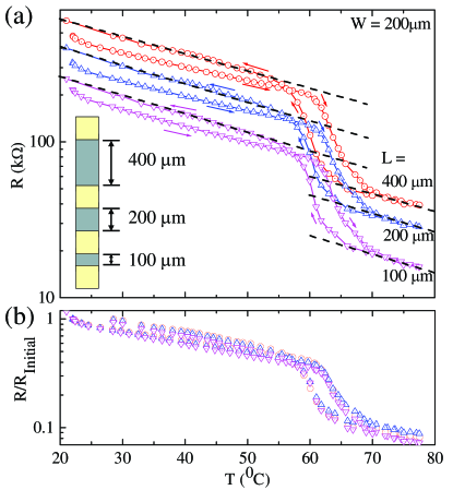
Devices of different lengths were photolithographically fabricated on the same substrate in order to facilitate length-dependence studies. Measurements are exhibited in Fig. 2(a), for a 400, a 200, and a long strip, with a width, . The noteworthy features in these data are once again that (i) in each case, the room temperature resistance after thermal cycling exceeds the initial room temperature resistance at the outset of the experiment, (ii) the width in of the hysteresis loop does not depend upon the length of the device, see also Fig. 2(b), (iii) in the low temperature phase, i.e., below , the variation of is linear in this vs plot, similar to the data in Fig. 1(a), and (iv) the same behavior continues onto the high temperature tetragonal, nominally ”metallic” phase, immediately above the structural transition.
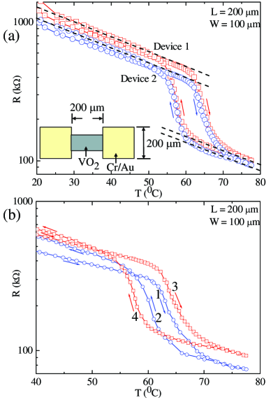
Identical devices on the same substrate also showed similar behavior on both sides of the structural transition; this is illustrated by the data of Fig. 3(a) for a pair of long wide devices.
As mentioned above, these measurements indicate an increase of the base temperature resistance upon thermal cycling. A close examination of such behavior revealed, in addition, a change in the width of the hysteresis loop, as exhibited in Fig. 3(b), especially over the first few thermal cycles. Figure 3(b) shows that the width of the hysteresis loop in the initial thermal cycle formed by the up sweep trace and the down-sweep trace measurements is roughly a factor of two smaller than width of the hysteresis loop observed in the second thermal cycle constituted by traces and . The figure also shows that in these measurements increases as one proceeds from data trace to to to . Thus, there appears to be a correlation between the increase in the base temperature upon thermal cycling and the broadening of the hysteresis loop over the range of characterizing the structural transition.
We present here a qualitative explanation, which builds upon earlier results. Berglund and Guggenheim reported long ago that single crystals of , and many other materials that exhibit a structural transition, include a tendency to fissure upon passing through the phase transition.4 The literature also demonstrates a strong correlation between the width of the hysteresis loop and the size of particles or grains in the system. Most recently, it has been shown that ensembles of nanometer sized particles exhibit a substantial hysteresis loop upon cycling through the transition,14 and this behavior was attributed to the reduced number of transition-triggering nucleation sites in smaller particles, and the consequent spread in transition temperatures in an ensemble of such small particles. The previous report of a wider hysteresis loop in smaller particles suggests the interpretation here that the increasing width of the hysteretic loop with repeated thermal cycling, see Fig. 3(b), originates from a reduction in the average grain size in thin films upon thermal cycling. Thus, the electrical response of these films seems to be a signature of transport through a granular network, and the increase in the base temperature resistance with thermal cycling seems to reflect the increased resistance in a grain-boundary dominated percolating network, as the grains become smaller, within a given device.
The other remarkable feature of these measurements on thin films is the similarity of the -dependence of on both sides of the structural transition. This feature is in sharp contrast to the behavior observed in high quality single crystals, where the structural transition brings with it also a metal-insulator transition.4 Note that the insulating state often exhibits activated transport, , and a divergent resistance in the limit, while the metallic state typically exhibits a finite in the limit. The observation in these experiments of a similar non-activated and non-metallic -dependence on both sides of the structural transition is therefore surprising. This feature suggests, perhaps, the absence of a true metallic state in these thin films.
We suggest here the conjecture that effective localization through the formation of small grains helps to transform the nominally ”metallic” state into a disorder mediated, relatively high resistance state with the characteristics. The hypothesis was advanced long ago that, in disordered single crystals, ”the so-called metallic phase [in ] is not metallic at all”.3 In that instance, Mott3 was referring to data1 from specimens showing just a one-to-two orders-of-magnitude change in over the structural transition. Perhaps, the disordered thin films examined in this study are physically similar to the single crystals then considered. The uniform temperature dependence then appears plausible here, however, if the -dependence of the coupling within the granular network sets the temperature dependence of the resistance on both sides of the structural transition.
Work at Harvard was supported by NSEC-Harvard under NSF PHY-0601184.
References
- (1)
- (2)