Anomalous giant piezoresistance in AlAs 2D electrons with anti-dot lattices
Abstract
An AlAs two-dimensional electron system patterned with an anti-dot lattice exhibits a giant piezoresistance (GPR) effect, with a sign opposite to the piezoresistance observed in the unpatterned region. We trace the origin of this anomalous GPR to the non-uniform strain in the anti-dot lattice and the exclusion of electrons occupying the two conduction band valleys from different regions of the sample. This is analogous to the well-known giant magnetoresistance (GMR) effect, with valley playing the role of spin and strain the role of magnetic field.
pacs:
72.20.-i, 73.23.Ad, 75.47.JnCurrently there is considerable interest in electronic devices whose operating principles go beyond the conventional, charge-based electronics. A prime example is the giant magnetoresistance (GMR) device BaibichPRL88 , one of the first members of a new class of ”spintronic” devices PrinzSci98 ; WolfSci01 whose operation rests on the manipulation of electron’s spin degree of freedom. In certain solids the electrons can reside in multiple conduction band minima (or valleys) and therefore have yet another, , degree of freedom. Here we report a giant, low temperature piezoresistance (GPR) effect in a two-valley AlAs two-dimensional electron system (2DES) patterned with anti-dot lattices. The effect is among the strongest seen in any system and allows the detection of minute strains and displacements via a simple resistance measurement. And yet it is anomalous as it has the opposite sign compared to the conventional piezoresistance found in multi-valley semiconductors SmithPR54 ; ShkolnikovAPL04 . Using magnetoresistance measurements and numerical simulations, we propose a model that qualitatively explains the observed GPR effect based on the non-uniform strain and the exclusion of electrons occupying the two conduction band valleys from different regions of the sample. This is analogous to the operating principle of the GMR effect: here valley plays the role of spin and strain the role of magnetic field. These results highlight the fundamental analogy between the spin and valley degrees of freedom GunawanPRL06 ; GunawanNP07 and point to new opportunities in developing novel ”valleytronic” devices whose functionality relies on the control and manipulation of the electron’s valley degree of freedom GunawanPRB06 ; RycerzNP06 .
We performed experiments on a 2DES in a modulation doped, 11 nm-wide AlAs quantum well. In this system the electrons occupy two in-plane, anisotropic conduction band valleys with elliptical Fermi contours PoortereAPL02 , characterized by a heavy longitudinal mass and light transverse mass , where is electron mass in vacuum. We label these as and valleys, according to the direction of their major axes, [100] and [010], as shown in the lower inset of Fig. 1 ShayeganPSSB06 . We patterned a Hall bar along the [100] direction using standard photo lithography technique. Then, via electron beam lithography and dry etching using an electron cyclotron resonance etcher we defined three anti-dot (AD) lattices with periods = 1, 0.8 and 0.6 m in three regions of the Hall bar, and left a fourth region un-patterned (blank) [see the upper insets of Fig. 1]. Each AD lattice is an array of holes (ADs) etched to a depth of 300 nm into the sample thus depleting the 2DES in the hole area (the 2DES is at a depth of 100 nm from the top surface). The ratio for each AD cell is 1:3, where is the AD diameter. We also deposited Ti/Au back- and front-gates to control the total 2DES density () in the sample. To apply tunable strain, we glued the sample to one side of a piezo-actuator ShayeganAPL03 , and monitored the applied strain using a metal-foil strain-gauge glued to the piezo’s other side. We define strain as where and are the fractional length changes of the sample along the [100] and [010] directions, respectively. Note that for electrons are transferred from the valley to the valley while stays constant ShayeganPSSB06 . Further fabrication details and characteristics of the blank region of the particular sample used in this study were reported in Ref. GunawanPRL06 . In particular, at a piezo bias () of -250 V, the and valleys in the blank region are equally occupied (balanced) and, at /cm2 where the data of Fig. 1 were taken, electrons are all transferred to the valley for V (); see the lower insets in Fig. 1. The measurements were performed in a 3He cryostat with a base temperature of 0.3 K.
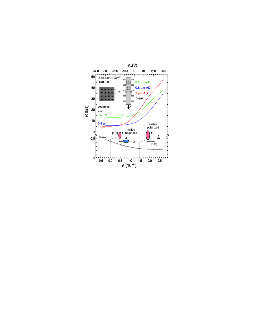
The lower trace in Fig. 1 shows the piezoresistance (PR) in the blank region. The PR exhibits the anticipated behavior: the resistance drops with increasing strain as the electrons are transferred to the valley whose mobility is higher (because of its smaller effective mass, ) along the current direction. Beyond the valley depopulation point ( ), the resistance starts to saturate at a low value as the intervalley electron transfer ceases. This is the conventional PR effect in AlAs 2DES as has been reported in Ref. ShkolnikovAPL04 . The dotted line in Fig. 1 represents the best fit of the data to a simple model ShkolnikovAPL04 , which assumes that the valley populations change linearly with strain, and adds the conductivities of the two valleys to find the total conductivity; the model also assumes an isotropic scattering time for both valleys and ignores the inter-valley scattering.
The upper three traces in Fig. 1 represent the PR of the AD regions and demonstrate our main finding. These traces exhibit an resistance as a function of strain, opposite to the PR in the blank region. The strength of the PR effect is also quite prominent in the AD regions: indeed, in the 1 m-AD region the resistance changes by about ten times for the range of applied strain while, in contrast, the change for the blank region is only about a factor of two. Furthermore, for all three AD regions, the PR persists beyond the valley depopulation point of the blank region ( 1.5) where the blank region’s PR nearly saturates.
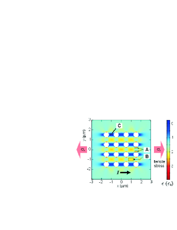
These observations highlight the remarkable difference between the PR effect in the blank and the AD regions and present an interesting puzzle. As we will now show, it is the presence of the AD lattice, which significantly modifies the strain distribution in the AlAs 2DES, that leads to the anomalous PR. To understand the strain distribution in the AD regions we performed a simple finite-element-method simulation (using FEMLAB) for a plane-strain problem of a 2D medium perforated with an array of holes. We apply a small tensile stress to the left and right sides, producing a small amount of strain at ; in other words, if there were no AD lattice, the strain would be uniform everywhere with a magnitude equal to . The result of this simulation is shown in Fig. 2. There is clearly a non-uniform strain distribution due to the presence of the AD lattice. In particular, there are localized regions of enhanced strain (boxes A and B in Fig. 2), and of essentially zero strain (box C). For example, in the upper and lower periphery of the AD (box A) the strain is enhanced by as much as 3. This enhancement by 3 is indeed indicated by an analytical solution of a 2D plane strain problem with a single hole SeeRoylance . We add that our simulation of Fig. 2 is for a 2D system, however, we expect that in a system which contains an AD lattice at its top surface, the strain profile is qualitatively similar to what is shown in Fig. 2.
But how does a non-uniform strain distribution lead to an increase in resistance? Note that, in our experiment, positive (negative) strain leads to a valley splitting that favors the valley ( valley) occupation. This means that electrons occupying either the or valley feel an extra, modulated, and confining potential (besides being excluded from the AD hole regions) as they move through the AD lattice. We believe that it is this potential that profoundly affects the quasi-ballistic motion of electrons in the AD region and leads to the observed PR. For example, consider the localized enhancement of positive strain in box A of Fig. 2. Such strain depletes the -valley electrons in box A and effectively narrows the width of the channels (between the holes) through which they have to travel to carry current to the right. In the remainder of the paper we present evidence from additional measurements and numerical simulations that lend further support to this picture.
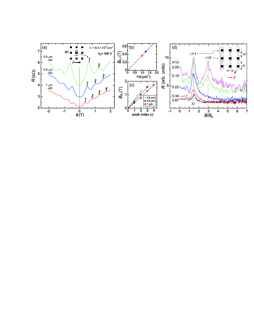
In Fig. 3(a) we show resistance vs. perpendicular magnetic field () traces for the three AD regions, taken at V (). Each trace exhibits a series of peaks that we label with indices = 1, 2, 3, … . These peaks are associated with the geometric resonance, or the commensurability, of the cyclotron orbits and the AD lattice period. Such commensurate orbits are well-known to occur in 2DESs with AD lattices WeissPRL91 ; GunawanPRB07 , although, as we discuss below, the presence of the 1 peaks is unusual. If we plot the positions of the peaks () vs. their indices as shown in Fig. 3(c), we observe that scales linearly with for all AD regions. We refer to the peak as the fundamental peak and peaks as the subharmonic peaks. First we focus our analysis of the fundamental peak and then present a detailed analysis of the subharmonic peaks.
Figure 3(b) presents a plot of the fundamental peak positions vs. the reciprocal AD lattice spacing . The observed linear dependence is consistent with the geometric scaling of the peak positions as expected from the relationship: , where is the Fermi wave vector of the commensurate orbit in the direction perpendicular to the current flow GunawanPRB07 . In fact, in Ref. GunawanPRB07 , systematic measurements and analysis of as a function of and were made in an AlAs 2DES with AD lattices but without any applied strain. Both experimental data and simulations showed that, while the two valleys and could in principle give rise to two sets of commensurate orbits, it is the X1 orbit [Fig. 3(a) inset] that gives rise to the fundamental magnetoresistance peak. The data in Fig. 3 are consistent with this finding: If we assign the fundamental peak to the Y1 orbit (similar to X1 except rotated by 90∘), we find that the corresponding -valley densities deduced from the positions of these peaks are unphysically large (greater than the total electron density, , determined from the Shubnikov de-Haas oscillations). We have repeated such analysis at various and , and have reached a similar conclusion. Therefore, we surmise that the fundamental peak is associated with the X1 orbit.
Now we focus on the sub-harmonic magnetoresistance peaks ( 1) observed in Fig. 3(a). Such peaks are observed in the absence of strain, e.g., in the experiments of Ref. GunawanPRB07 , and their presence in Fig. 3(a) traces in fact provides clues for the shape of the potential seen by the -valley electrons in the present sample. While subharmonic peaks are seldom seen in AD lattices, they are readily observed in transverse magnetic focusing (TMF) experiments vanHoutenPRB89 ; NiheyAPL90 where ballistic electrons are emitted through a narrow opening and are collected at a second narrow opening which is at a relatively large distance away. Under such conditions, the injected ballistic electrons can bounce off the TMF barrier one or more times as they follow their cyclotron orbit trajectories, and magnetoresistance peaks are observed whenever the emitter-collector distance equals a multiple integer of the orbit diameter (an illustration of this is shown in Fig. 3(d) inset for our structure.) We emphasize that in TMF structures, the distance between the emitter and collector is typically larger than the width of the emitter and collector openings thus allowing bouncing trajectories to occur. Furthermore, the narrow openings also produce better focusing and therefore sharp subharmonic peaks.
We hypothesize that the subharmonic peaks observed in Fig. 3 data arise from an effective narrowing of the ”emitter and collector openings” and an elongation of the effective AD boundary for the -valley electrons upon the application of strain as shown in Fig. 3(d) inset. This is clearly suggested by the simulations of Fig. 2 where the -valley electrons are excluded near the lower and upper boundaries of the ADs (box A) because of the larger local strain. Several features of Fig. 3 data support this hypothesis: (1) As shown in Figs. 3(c) and (d) all the peak positions are consistent with the orbit diameters being proportional to . (2) The sub-harmonic peaks are pronounced only when strain is applied: Their amplitudes are indeed small near zero strain, increase with , and then saturate. (3) The AD region with the largest period (i.e. the 1 m-AD) has the most sub-harmonic peaks; this is consistent with the longer AD boundary allowing more bounces in the electron trajectories.
To further test our conjecture, we performed numerical simulations similar to those used in Ref. GunawanPRB07 but with a variable channel width to simulate the strain-induced channel-pinching effect circle_vs_square . The results, presented in Fig. 3(d), verify our conjecture that a smaller indeed gives rise to a second sub-harmonic peak that grows in amplitude relative to the fundamental peak. Note also that, as might be expected, Fig. 3(d) simulations show an overall increase in resistance at = 0 for narrower channels, consistent with the PR data of Fig. 1.
Our experimental data and the numerical simulations combined strongly suggest a ”channel-pinching effect” in the strained AD lattice for the -valley electrons. Such an effect explains the emergence of the sub-harmonic commensurability peaks in the magnetoresistance and also the zero-field PR. However, our model leaves an important question unanswered: What is the role of the -valley electrons which in fact become the majority carriers and dominate the transport in the blank region with increasing (lower trace in Fig. 1)? It is likely that the non-uniform strain in the AD region creates a strong modulating potential, limiting the conductivity of the -valley electrons. An increase of resistance with the increase of potential modulation amplitude is indeed common in commensurability oscillation experiments on surface grating devices BetonPRB90 . It is conceivable that although -valley electrons are favored at high strains, their contribution to the overall AD lattice conductivity is suppressed by the strongly modulated potential.
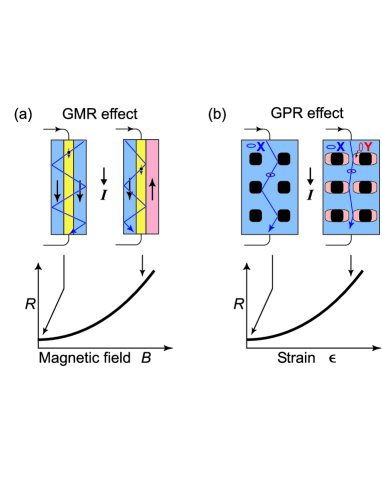
The above channel-pinching picture suggests a remarkable resemblance between our GPR effect and the GMR effect, observed in thin-film structures composed of alternating layers of ferromagnetic and non-magnetic materials PrinzSci98 ; EgelhoffJVST99 . A comparison of these two effects is schematically illustrated in Fig. 4. In each structure, the reversal of polarization of the magnetization (spin) or valley in the regions adjacent to the active channel due to either external magnetic field () or applied strain () leads to a narrower effective channel width (extra confinement) and possibly additional scattering (for both and -valley electrons) both of which lead to higher resistance.
Regardless of its origin, the GPR exhibited by our AD lattices reveals the extreme sensitivity of their resistance to strain. The data of the 1 m AD lattice, e.g., yield a maximum strain gauge factor, , defined as the fractional change in sample resistance divided by the fractional change in sample length, of over 20,000. This is by far larger than of standard, metal foil gauges, and is among the largest reported for any solid state material. Our structure may find use as an extremely sensitive, low-temperature PR strain sensor to detect ultrasmall forces and distances. Using a simple resistance measurement, we were able to detect strains down to with our samples GunawanThesis07 . Given that the spacing between our Hall bar resistance contacts is 40 m, this strain translates to a displacement of 810-4 nm (about 1/50 of the Bohr radius)! This sensitivity could be further improved by designing AD lattices with optimized shapes and sizes, and using more sophisticated techniques to measure resistance changes.
We thank the ARO and NSF for support, and K. Vakili for illuminating discussions.
References
- (1) M. N. Baibich et al., Phys. Rev. Lett. 61, 2472 (1988).
- (2) G. A. Prinz, Science 282, 1660 (1998).
- (3) S. A. Wolf et al., Science 294, 1488 (2001).
- (4) C. S. Smith, Phys. Rev. 94, 42 (1954).
- (5) Y. P. Shkolnikov et al., Appl. Phys. Lett. 85, 3766 (2004).
- (6) O. Gunawan et al., Phys. Rev. Lett. 97, 186404 (2006).
- (7) O. Gunawan et al., Nat. Phys. 3, 388 (2007).
- (8) O. Gunawan et al., Phys. Rev. B 74, 155436 (2006).
- (9) A. Rycerz et al., Nat. Phys. 3, 172 (2006).
- (10) E. P. De Poortere et al., Appl. Phys. Lett. 80, 1583 (2002).
- (11) M. Shayegan et al., Phys. Stat. Sol. (b) 243, 3629 (2006).
- (12) M. Shayegan et al., Appl. Phys. Lett. 83, 5235 (2003).
- (13) See, e.g., D. Roylance, Mechanics of Materials (Wiley, New York, 1995) p. 186.
- (14) D. Weiss et al., Phys. Rev. Lett. 66, 2790 (1991).
- (15) O. Gunawan et al., Phys. Rev. B 75, 81304(R) (2007).
- (16) H. van Houten et al., Phys. Rev. B 39, 8556 (1989).
- (17) F. Nihey et al., Appl. Phys. Lett. 57, 1218 (1990).
- (18) For simplicity and also because the drawn shape of each AD was intended to be a square, in the simulations of Fig. 3(d) we used square and rectangular shapes for the ADs as indicated in the figure. We repeated the simulations with circular and elliptical AD shapes and obtained qualitatively similar results.
- (19) P. H. Beton et al., Phys. Rev. B 42, 9229 (1990).
- (20) W. F. Egelhoff et al., J. Vac. Sci. Tech. B 17, 1702 (1999).
- (21) O. Gunawan, Ph.D. thesis, Princeton University (2007).