A three-dimensional backward-wave network matched with free space
Abstract
A backward-wave slab based on a capacitively and inductively loaded three-dimensional transmission-line network is designed in such a way that impedance-matching with free space is obtained. To enable field propagation from free space to the network and vice versa, the use of a transition layer is proposed. Matching of the designed network with free space and negative refraction occurring at the slab interfaces are confirmed with full-wave simulations.
I Introduction
As suggested by Veselago,Veselago a material with negative permittivity and permeability (a backward-wave material) can be used as a flat lens that focuses propagating electromagnetic waves. Due to the negative and , the wave propagation in this material differs significantly from any material found in nature, since the phase and group velocities are antiparallel. Furthermore, as shown by Pendry,Pendry a slab of such material can be used as a superlens that, besides focusing the propagating waves, enhances the evanescent waves of a source.
First experimental demonstration of negative refraction, that occurs on the interface between a material with positive and and a material with negative and , was achieved with a slab made of a composite material consisting of metal wires and split-ring-resonators.Shelby The use of resonant particles in creating the wanted negative has the drawback of very narrow operation bandwidth and high sensitivity to losses. An alternative approach to creating a “material” with negative and , based on loaded transmission lines (TLs), has been proposed.Eleftheriades ; Caloz The benefit of this approach is the fact that the exotic wave propagation is not due to use of resonant particles and thus the operational bandwidth and losses are not so critical issues. The drawback of such structures in superlens applications is that coupling of waves from free space to such a network is not trivial. Indeed, superlenses proposed in the literature that are based on the TL-method, have used sources which are embedded in a TL network as well, see e.g. Ref. 6. Recently, also three-dimensional extensions of the TL-method have been proposedGrbic2 ; Hoefer ; Alitalo1 and realized.Alitalo2
Recently, a design of a TL network with negative index of refraction, that can be matched with free space, was proposed.Iyer This approach can be realized for two-dimensional TL networks, i.e., a set of two-dimensional TL networks can be stacked on top of each other creating a volumetric slab. In this letter, we propose a transition layer to couple waves from free space to a TL network such as proposed in Ref. 6 (two-dimensional TL network) and in Ref. 9 (three-dimensional TL network). The transition layer is effectively an array of antennas that covers the whole interface between free space and the TL network. This approach, as compared to the previous design,Iyer has the benefit of freedom in the design of the TL network, since the network itself does not have to be coupled with free space. Moreover, there are no parasitic forward waves, since fields are concentrated in the TLs only.
II Design of the loaded transmission-line network
In this letter we study the structure presented in Refs. 9 and 10, although the proposed method of matching a TL network with free space can be used for other types of networks as well.cloak As compared to the previous designs,Alitalo1 ; Alitalo2 here we do not have an unloaded network representing free space, but instead, a transition layer that enables electromagnetic waves from free space to propagate into the TL network and vice versa.
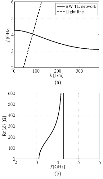
To optimize matching with free space, we need to design the TL network in such a way that its impedance equals that of free space (377 ). Using the previously derived dispersion and impedance equations,Alitalo1 we have found suitable dimensions and parameters for the network operation in the microwave region, see Table I. The resulting dispersion and impedance curves are presented in Fig. 1. From Fig. 1 we can conclude that the optimal operation frequency for the network studied here is around 4 GHz. The operation frequency can be changed e.g. by varying the values of the lumped capacitances and inductances.
| Period | TL impedance | |||
|---|---|---|---|---|
| 8 mm | 0.1 pF | 2.5 nH | 1 |
III Transition layer and simulation model
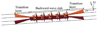
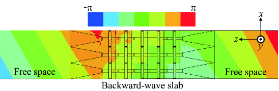
As the TL network that is used here is similar to previous designsAlitalo1 ; Alitalo2 it can be conveniently realized using the microstrip technology. The transition layer can therefore be realized with parallel-plate-waveguide type of TLs at the ends of the network, as illustrated in Fig. 2. Naturally, this way we can obtain operation for one polarization only.Iyer The benefit of this method is its simplicity. We study a slab composed of the three-dimensional TL network (infinite in the transversal directions in this case) and the TLs of the transition layer cover the both surfaces of the slab.
We have made full-wave simulations of the proposed backward-wave slab with the transition layers and sections of free space on both sides of the slab. The simulations were done using Ansoft’s High Frequency Structure Simulator (HFSS). The simulation of the transversally infinite slab can be greatly simplified by using periodical boundary conditions. This way we can simulate only one “unit cell” of the slab, as shown in Fig. 2. The TL network has the same parameters as shown in Table I. The metal strips are made of infinitely thin perfect conductors and have the width of 1.3 mm with the distance from the ground being 2 mm. Small holes are cut into the horizontal and vertical ground planes to allow wave propagation in all axial directions. As shown in Fig. 2, the thickness of the slab is five periods in the direction of the -axis. The width of the TLs of the transition layer gradually changes from 2 mm to 7.988 mm, with their length being 16 mm. The neighboring TLs of the transition layer are not in contact, since there are approximately 12 and 4 gaps between them in the - and -directions, respectively.
IV Simulation results
First, the case of the normal incidence was studied, i.e., a plane wave in free space with the wave vector parallel to the -axis and electric field parallel to the -axis illuminated the backward-wave slab. By studying the reflection () and transmission () coefficients, it was found that the optimal operation frequency for the structure was approximately 3.6 GHz (the frequency point where most of the power went through the slab). This implies that the impedance of the network was best matched to free space at that frequency, since the transition layer impedance does not depend on the frequency. By changing the inductance value of the lumped inductances to nH, the reflection and transmission curves shown in Fig. 3 were obtained, showing good correspondence with Fig. 1(b).
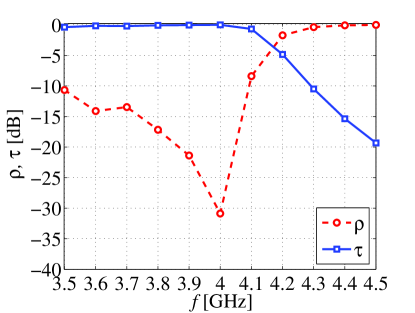
We believe that the slight difference in the inductance value with which operation at 4 GHz is achieved, as compared to the analytical study, is a result of differences between the analytical and simulation models. The analytical equations do not take into account the finite size of the lumped elements and the equations used to calculate the data presented in Figs. 1(a) and 1(b) do not take into account the finite thickness of the slab.Alitalo1 The study of this inaccuracy is out of the scope of this letter, since here we wish to illustrate the feasibility of the proposed matching method as such.
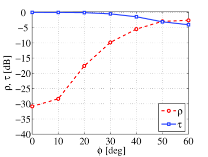
From Fig. 3 it is seen that the optimal frequency of operation (for normal incidence) is approximately 4 GHz. To study the dependence of the transmission and reflection on the incidence angle, we have made simulations with the same model for oblique plane-wave illumination. The polarization of the illuminating wave is kept the same, i.e., is parallel to the -axis and therefore the incidence angle is the angle in the -plane. See Fig. 4 for the results when . We can conclude that the transition layer operates very well also for fairly large oblique incidence angles, although the transmission clearly reduces when grows.
With the model shown in Fig. 2 the refraction on the interface between free space and the backward-wave slab may not be visible due to the small size of the model in the transversal direction. To observe negative refraction, we have extended the simulation model to encompass three “unit cells” of the slab in the -direction. See Fig. 5 for the simulated phase distribution in this larger simulation model at the frequency 4 GHz and incidence angle of . The relative refractive index of the slab seems to be close to , which is expected based on the dispersion curve in Fig. 1(a).
Preliminary simulations show that at least for small angles of incidence also in the -plane (angle ), the transition layer operates well. For instance, for the incidence angle of (with ) the reflection from the backward-wave slab is below dB at the frequency 4 GHz.
V Conclusions
We have proposed and studied a transition layer for matching a slab of a backward-wave transmission-line network with free space. We have analytically studied how the network impedance can be tuned to match that of free space. The proposed network and transition layer have been simulated using a commercial full-wave simulator. The simulation results show that the layer can be used to match a backward-wave transmission-line network with free space and verify the negative refraction on the interfaces between free space and the network.
Acknowledgements
This work has been partially funded by the Academy of Finland and TEKES through the Center-of-Excellence program. Pekka Alitalo wishes to thank the Graduate School in Electronics, Telecommunications and Automation (GETA) and the Nokia Foundation for financial support.
References
- (1) V. G. Veselago, Sov. Phys. Usp., 10, 509 (1968).
- (2) J. B. Pendry, Phys. Rev. Lett., 85, 3966 (2000).
- (3) R. A. Shelby, D. R. Smith, and S. Schultz, Science, 292, 77 (2001).
- (4) G. V. Eleftheriades, A. K. Iyer, and P. C. Kremer, IEEE Trans. Microwave Theory Tech., 50, 2702 (2002).
- (5) C. Caloz, H. Okabe, T. Iwai, and T. Itoh, Proc. USNC/URSI National Radio Science Meeting, 1, 39, June 2002,
- (6) A. Grbic and G. V. Eleftheriades, Phys. Rev. Lett., 92, 117403 (2004).
- (7) W. J. R. Hoefer, P. P. M. So, D. Thompson, and M. M. Tentzeris, 2005 IEEE MTT-S International Microwave Symposium Digest, 313, June 2005.
- (8) A. Grbic and G. V. Eleftheriades, J. Appl. Phys., 98, 043106 (2005).
- (9) P. Alitalo, S. Maslovski, and S. Tretyakov, J. Appl. Phys., 99, 064912 (2006).
- (10) P. Alitalo, S. Maslovski, and S. Tretyakov, J. Appl. Phys., 99, 124910 (2006).
- (11) A. K. Iyer and G. V. Eleftheriades, 2006 IEEE MTT-S International Microwave Symposium Digest, 428, June 2006.
- (12) P. Alitalo, L. Jylhä, A. Karttunen, O. Luukkonen, G. Molera, H. Rimminen, M. Vaaja, J. Venermo, V. Podlozny, A. Sihvola, S. Tretyakov, and H. Wallén, “Realization of an electromagnetic invisibility cloak by transmission-line networks,” Proc. Metamaterials ’2007, 22-26 October 2007, Rome, Italy, to be published.