Dielectric microscopy of with submillimeter resolution
Abstract
In analogy with optical near-field scanning methods, we use tapered dielectric waveguides as probes for a millimeter wave vector network analyzer. By scanning thin samples between two such probes we are able to map the spatially varying dielectric properties of materials with sub-wavelength resolution; using a 150 GHz probe in transmision mode we see spatial resolution of around 500 microns. We have applied this method to a variety of highly heterogeneous materials. Here we show dielectric maps of granite and oil shale.
I Introduction
Near-field scanning optical microscopy (NSOM) is an established technique for achieving nano-scale resolution of surface material properties (nsombook, ). Recently these ideas have been extended to millimeter waves; that is, electromagnetic waves spanning roughly from 30 to 300 GHz (e.g., (nozokido:148, ), (kume:056105, )). In particular, Kume and Sakai (kume:056105, ) used a dielectric probe machined from Teflon. We apply a very similar technique with conical Teflon probes on either side of thin sections of rocks. This allows us to achieve transmission-mode dielectric maps of rocks with submillimeter resolution, limited in speed only by the mechanical scanning stages.
II Setup
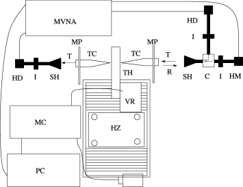
Fig. 1 shows the experimental setup, which is based on a millimeter wave vector network analyzer (MVNA) made by AB Millimetre of France. The MVNA generates stabilized centimeter waves (8-18 GHz) phase locked to a rubidium standard which are then converted to millimeter waves (MMW) as they pass through a harmonic multiplier. From here the MMW propagate via single mode wave guide and are radiated from a scalar (or corrugated) horn. In the wave guide the E field is in a TE01 mode and is vertically polarized. The effect of the scalar horn is to produce a axially symmetric radiation pattern with no cross-polarization. This is a hybrid mode (goldsmith, ).
The free-space MMW are then coupled into a Teflon cone which acts as a near-field probe placed near the surface of the sample. The cone is inserted through a small opening in an aluminum plate to prevent diffraction around the probe. Teflon is used due to its high transparency at microwave and millimeter wave frequencies. The E field transmitted through the sample is coupled to another Teflon cone, which in turn couples to a scalar horn. The transmitted field is then detected via a harmonic detector driven by a local oscillator. The reflected wave goes back through the first cone and scalar horn and then via a circulator to a second harmonic detector. All the microwave oscillators are phase locked to the Rubidium clock. For more details see (scales_batzle_apl2, ), (mmwaves_expt, ).
Holding the sample between the cones is a Teflon holder attached to two linear motors. One is positioned vertically while the other is positioned horizontally. Both of the motors are connected to a Newport controller, which is controlled by a computer running LabView.
The idea behind the measurement is that as the probe scans the surface of a heterogeneous sample, the phase of the transmitted E field is perturbed in proportion to changes in the local index of refraction (assuming a constant thickness sample). Hence a spatial map of the phase of the E field can be directly translated into a spatial map of local variations in the index of refraction. Perturbations in the index of refraction (a size-independent material property) can be related to perturbations in the transmitted phase via
where is the thickness of the sample. In all cases the measured phase angles have been unwrapped.
III Experiment
III.1 Benchmark: perfboard
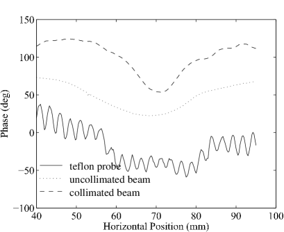
As a first test of the system we use a piece of perforated circuit board (a synthetic resin bonded paper with no conductive soldering tabs) as a benchmark. The soldering holes (Fig. 2) are drilled on a 2.56 mm centers. In addition to the holes, we put 6 layers of masking tape on the perfboard to create a linear feature.
As can be seen from Fig. 2 after scanning across the sample, the holes themselves cannot be seen with either the collimated or uncollimated 150 GHz beam. The index change due to the tape is smeared out over a distance of around 20 mm, which is the beam width. However, with the Teflon probes both the holes and the tape can be easily resolved. The free-space wavelength at 150 GHz is 2 mm. Fig. 2 suggests a resolution of at least , or around 500 m.
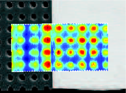
With the ability to see the holes in a linear scan, we moved up to a two dimensional scan to produce Fig. 3, which shows an overlay of the phase contrast map and an optical scan of the perfboard. In the two dimensional scan, you can clearly see the holes and also the change from only circuit board to circuit board with tape.
III.2 A strongly heterogeneous medium
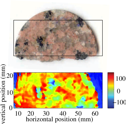
After these preliminary benchmarks we next scanned some granular materials that we have previously used in studies of wave propagation in random media ((scales_batzle_apl2, ), (mmwaves_expt, ), (PhysRevE.67.046618, ), (malcolm:015601, )) For the first scan we chose to use a piece of medium grained granite (Llano granite). In the top of Fig. 4 an optical scan of the sample shows the main constituents of this granular sample: the black grains are biotite (a common mineral within the mica group), the gray grains are quartz (silica) and the pink grains are feldspar (a common mineral crystallized from magma that makes up a large fraction of the Earth’s crust).
Scanning over a piece that is uniformly 2.13 mm thick gave us Fig. 4. Correlating the optical scan and the phase map it is apparent that the red colors (large positive phase perturbations) corresponds to quartz grains. The green color (relative phase of zero degrees) corresponds to Feldspar. The bluish color (large negative phase perturbation) corresponds to biotite. Since the sample is about 2 mm thick (i.e., one ), a phase change corresponds to an index change of about Previously measured (vaccaneo, ) microwave values of the index for Quartz (2.05 - 2.23) and Mica (2.16 - 3.0) are consistent with these measured phase changes.
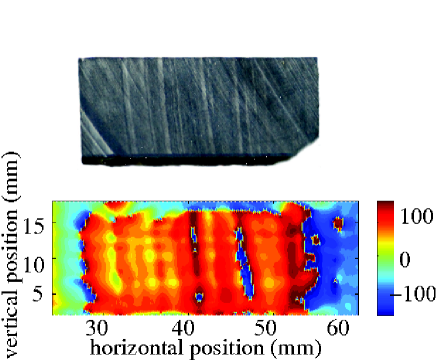
III.3 A finely laminated medium
A sedimentary rock, such as oil shale, can show millimeter scale lamination. The birefringence caused by this layering was previously discussed in (scales_batzle_apl2, ). By doing the same scan on a 4.44 mm thick piece of oil shale as we did on the granite, we were able to see changes in the phase when moving from organic-rich areas to organic-poor areas in the oil shale. As Fig. 5 shows, we were able to resolve dielectric changes of less than a millimeter across. The phase change in this figure going from blue to red is about 3.5 radians. This corresponds to an index change of This is very close to the index differences seen (scales_batzle_apl2, ) for homogeneous samples of oil-rich and oil-poor shale.
IV Conclusion
By using an easily manufactured conical Teflon probe we were able to greatly enhance the spatial resolution of our quasi-optical millimeter wave setup via a near-field scanning probe technique. This continuous wave technique has extremely high sensitivity to small index-induced phase changes of the transmitted electric field. We tested this technique on strongly heterogeneous granular samples (metamorphic and sedimentary rocks) and were able to obtain resolution of around 500 microns using a 150 GHz probe. The technique is fast (limited only by the speed of the mechanical scanning) and is easily applied to any free space quasi-optical system. Many other applications suggest themselves, including near-field measurements of planar antennae, integrated circuits, and other amorphous materials.
Acknowledgements
This material is based upon work supported by the National Science Foundation under Grant EAR-0337379.
References
- (1) M. Ohtsu and K. Kobayashi, Optical Near Fields: Introduction to Classical and Quantum Theories of Electromagnetic Phenomena at the Nanoscale (Springer, Berlin, 2004).
- (2) T. Nozokido, J. Bae, and K. Mizuno, Applied Physics Letters 77, 148 (2000).
- (3) E. Kume and S. Sakai, Journal of Applied Physics 99, 056105 (2006).
- (4) P. Goldsmith, Quasioptical systems: Gaussian beams quasioptical propagation and a pplications (IEEE Press, New York, NY, 1998).
- (5) J. A. Scales and M. Batzle, Applied Physics Letters 89, 024102 (2006).
- (6) J. A. Scales and M. Batzle, Applied Physics Letters 88, 062906 (2006).
- (7) J. A. Scales and A. E. Malcolm, Phys. Rev. E 67, 046618 (2003).
- (8) A. E. Malcolm, J. A. Scales, and B. A. van Tiggelen, Physical Rev. E 70, 015601 (2004).
- (9) D. Vaccaneo et al., IEEE Transactions on Geoscience and Remote Sensing 42, 2490 (2004).