Quenched magnetic moment in Mn-doped amorphous Si (a-MnxSi1-x) across the metal-insulator transition
Abstract
The magnetic and electrical transport properties of Mn-doped amorphous silicon (a-MnxSi1-x) thin films have been measured. The magnetic susceptibility obeys the Curie-Weiss law for a wide range of (0.005-0.175) and the saturation moment is small. While all Mn atoms contribute to the electrical transport, only a small fraction (interstitial Mn2+ states with ==5/2) contribute to the magnetization. The majority of the Mn atoms do not possess any magnetic moment, contrary to what is predicted by the Ludwig-Woodbury model for Mn in crystalline silicon. Unlike a-GdxSi1-x films which have an enormous negative magnetoresistance, a-MnxSi1-x films have only a small positive magnetoresistance, which can be understood by this quenching of the Mn moment.
pacs:
68.55.-a, 75.50.Pp, 71.23.Cq, 61.43.DqI introduction
Mn has been widely used as a magnetic dopant in dilute magnetic semiconductors (DMS), which have potential applications as spintronic materials. While many Mn-doped systems are antiferromagnetic (AFM), ferromagnetism was found in Mn-doped III-V semiconductors, such as GaMnAs, first reported by Ohno Ohno (1998). Both mean-field theory (Zener model) Dietl et al. (1998) and first-principles calculations Stroppa et al. (2003); Bernardini et al. (2004); Weng and Dong (2005) have predicted that room temperature ferromagnetism is possible in Mn-doped group-IV semiconductors. An empirical rule is that short range Mn-Mn direct interaction favors AFM coupling, while long-range indirect interactions (RKKY, double exchange, kinetic exchange) favors ferromagnetic ordering. Interactions and mixing of the Mn d electrons in different host environments will lead to different charge and spin states, which greatly affect the magnetic ordering Weber (1983). There is a strong recent focus on research into Mn-doped crystalline Ge (c-Ge) and Si (c-Si) Park et al. (2002); Kang et al. (2005); Kwon et al. (2005); Bolduc et al. (2005); Awo-Affouda et al. (2006); Zhou et al. (2007). Mn-doped c-Si, in particular, is of much interest due to its compatibility with Si-based semiconductor technology. However, the solubility of Mn in crystalline group-IV semiconductors is extremely low. Therefore, to stabilize Mn doping above the solid solubility limit, one must utilize highly non-equilibrium doping techniques such as low temperature molecular beam epitaxy (MBE) Zhang et al. (2005) or ion-implantation Weber (1983); Park et al. (2002). Recent studies on Mn-implanted crystalline Si (c-Si1-x:Mnx) thin films prepared by the latter technique have achieved Mn doping levels of a few atomic percent (0.05) Kwon et al. (2005); Bolduc et al. (2005).
Ferromagnetism [Curie temperature () up to 116 K] was observed in Mn-doped c-Ge (c-MnxGe1-x) and a long-range ferromagnetic (FM) interaction dominating over a short-range Mn-Mn AFM interaction was proposed as the origin of the ferromagnetism Park et al. (2002). Determining whether the ferromagnetism in Mn-doped c-Ge and c-Si is intrinsic or not in origin, is however, very challenging due to thermodynamically favorable FM second phases or possible nano-structures, which are hard to detect by conventional structural characterization tools. Recent studies, including sub-micron scanning photoelectron microscopy (SPEM), high-resolution transmission electron microscopy (HRTEM) and synchrotron x-ray diffraction, have shown chemical inhomogeneity in c-Ge1-xMnx Kang et al. (2005) and the existence of MnSi1.7 nano-crystallites in c-Si1-x:Mnx Zhou et al. (2007). The ferromagnetism in these systems was attributed to a Mn-rich Ge phase Kang et al. (2005) and MnSi1.7 nano-crystallites Zhou et al. (2007) in the former and latter systems, respectively.
One way to stabilize homogeneous Mn doping is to prepare the film in the amorphous form. A strong attraction of a high quality amorphous matrix is its outstanding flexibility to incorporate high concentration of dopant atoms with large radius, such as Gd Zeng et al. (2007). For up to 19 at.% Gd doping, the structure of the Gd-Si solid solution is arranged such that its atomic number density is almost the same as that of pure amorphous Si (a-Si). While the amorphous structure may alter the long-range magnetic ordering (especially for AFM materials), the localized magnetic moment at each doping site should still be preserved since charge and spin states are primarily determined by the local environment. Instead of directly addressing the question of whether the final solid-state is ferromagnetic, antiferromagnetic or paramagnetic, it is conceptually easier to understand the existence of local magnetic states, which are the building blocks for more complicated magnetic interactions and orderings. This conceptual simplification was suggested to be of great value in understanding the ferro- and antiferro-magnetism in transition-metal solid solutions Anderson (1961), and may also apply to the study of transition-metal-doped semiconductor alloys.
Metallic dopants in amorphous semiconductors can also provide charge carriers from delocalized and electrons, which contribute to the electrical conductivity. A concentration-tuned metal-insulator (M-I) quantum phase transition has been reported in a variety of doped amorphous semiconductors, such as a-NbxSi1-x Hertel et al. (1983), a-GdxSi1-x Teizer et al. (2000a, b) and a-GdxGe1-x Sinenian et al. (2006). In M-I physics, a metal is defined as having finite dc conductivity () as 0 K, whereas an insulator is defined by 0 when 0 K. If the dopant has a large local moment, such as Gd3+ with ==7/2, thin film samples will have an enormous negative magnetoresistance (MR105 at 1 K), which leads to a magnetic-field-induced M-I transition in a-Gd-Si and a-Gd-Ge alloys Teizer et al. (2000b); Sinenian et al. (2006). The mechanism for this enormous negative MR is not fully understood, but is clearly related to a carrier-moment exchange interaction and magnetically-induced disorder in zero magnetic field which leads to carrier localization. Electron correlation effects and electron screening have been suggested to play an important role Helgren et al. (2005) in the magnitude of the MR and its onset temperature, denoted as .
There have been limited reports about Mn-implanted a-Si (denoted as a-Si1-x:Mnx), mainly focusing on transport properties for 0.07-0.22 Yakimov et al. (1995, 1997); Yakimov and Dvurechenskii (1997). Samples were prepared by room-temperature Mn ion-implantation either into -beam-evaporated a-Si on quartz (0.13) Yakimov et al. (1995) or into c-Si on sapphire with simultaneous amorphization of the films (0.13) Yakimov et al. (1997). No magnetic properties were reported. However, a characteristic temperature was observed in the transport data, which was attributed to spin-glass (SG) ordering by - spin correlation between Mn atoms. The characteristic SG temperatures () were not confirmed by magnetization measurements, but were estimated from the cross-over temperature between a variable-range hopping (VRH) behavior and a simple-activated behavior obtained from dc conductivity data fitting. From this analysis, was claimed to vary from 6 to 20 K, depending on the Mn concentration. This is rather high compared to that found in amorphous MnSi (=0.5), with SG freezing at =22 K. Such high requires a local Mn moment with - exchange interactions. These results were explained by AFM ordering of small magnetic clusters and magnetic polaron formation within the Mn clusters. The a-Si1-x:Mnx films undergo an M-I transition at a similar critical composition (0.137 Yakimov and Dvurechenskii (1997)) as for a-GdxSi1-x, but there is no large MR effect Yakimov et al. (1995); the obvious difference is d vs f electron magnetism. The MR must be related to an exchange interaction between carriers and moments. Therefore, it is puzzling that MR would be smaller in a material with electrons (a-Mn-Si) than one with electrons (a-Gd-Si) since - exchange is typically much larger than - exchange.
Ludwig and Woodbury have developed a model to predict the spin and charge states of 3 transition metals within c-Si Ludwig and Woodbury (1960). The Ludwig-Woodbury (LW) model states that crystal-field splitting is small in c-Si compared to the on-site exchange energy, so that all 3 impurities have a maximum spin value (Hund’s rule). The LW model was later challenged for the early and late transition metals such as Ni and Ti, but is still believed to account for Mn impurities. Electron-spin resonance (ESR) experiments confirmed the spin states of four different charge states for interstitial Mn (Mn, Mn, Mn and Mn) Weber (1983), all consistent with the LW model. The 4 nearest neighbors (tetrahedral symmetry) and the 6 second nearest neighbors (octahedral symmetry) of an interstitial site in c-Si are very close together and thus both sets of neighbors take part in determining the crystal-field splitting. This splits the levels into and levels, with levels lying higher than levels. Spin states of the two possible substitutional states (Mn and Mn) proposed by the LW model have not been observed by ESR measurements, but would have ==1 and ==5/2, respectively. The levels lie higher than the levels for both Mn states. In a-Si, the site symmetry is lowered due to disorder. The effect on the crystal field splitting due to the disorder is unknown.
We report here on Mn-doped amorphous silicon (a-Mnx-Si1-x) thin films, with between 0.005 to 0.175, covering both the dilute and the M-I transition regions. The films were prepared by -beam co-evaporation of Mn and Si under ultrahigh vacuum (UHV) conditions. Co-deposited a-MnxSi1-x samples have a much more homogeneous Mn distribution in the a-Si matrix compared to that of implanted samples, and should thus provide a better representation of the behavior of this type of amorphous solid solution. The focus of this current work is to understand the magnetic and magneto-transport properties of Mn dopants in a-Si, especially the presence or absence of any local Mn moment and its effect on electrical transport.
II experimental details
The a-MnxSi1-x samples were grown by -beam co-evaporation of high purity Si and Mn sources onto substrates held near room temperature (below 60 ∘C during film growth). This condition is in contrast to the film preparation described in Refs. Bolduc et al., 2005 and Zhou et al., 2007, where the substrates were held at 350 ∘C to avoid amorphization, and post-implantation annealing (up to 800 ∘C) was used to create c-Si1-x:Mnx films. Our base pressure prior to deposition was below 810-10 Torr. Thickness monitors were used for each source during deposition in order to precisely control the real-time Mn and Si flux to achieve uniform doping profiles as well as the desired Mn concentrations. The film compositions and lack of oxygen impurities were determined by Rutherford backscattering (RBS), using oxygen-resonance energy to enhance sensitivity, and by high-resolution cross-sectional transmission electron microscopy (HR-XTEM). Magnetic and magneto-transport measurements were made with a superconducting quantum interference device (SQUID) magnetometer from Quantum Design. Further details can be found in Ref. Zeng et al., 2007.
III Experimental Results
III.1 Material and Structural Characterization
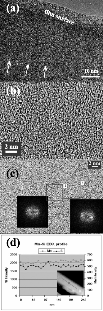
Figure 1 shows HR-XTEM analysis for a typical a-MnxSi1-x film, where =0.11. The film shows columnar morphology in the growth direction, a typical feature for low thermally evaporated thin films Zeng et al. (2007), with column diameters 10 nm [Fig. 1(a)]. The physical transport and magnetic properties were shown experimentally to not depend on microstructure at this length scale in amorphous Gd-Si alloys prepared by the same growth technique Zeng et al. (2007). The a-MnxSi1-x films appear to be amorphous with no significant sign of phase segregation or nano-crystallites. Figure 1(b) shows a slight suggestion of lattice fringes for regions of less than 2 nm; but digital diffractograms show typical amorphous rings, indicating absence of long-range ordering [Fig. 1(c)]. Annular-dark-field (ADF) images with energy-dispersive X-ray (EDX) spectroscopy were also used to probe the homogeneity of the a-MnxSi1-x films. As an example, Fig. 1(d) shows the variation of Mn and Si counts along a 250 nm line parallel to the film surface. The Mn distribution was uniform along the scanning length, with no strong indication of significant fluctuation in Mn concentration.
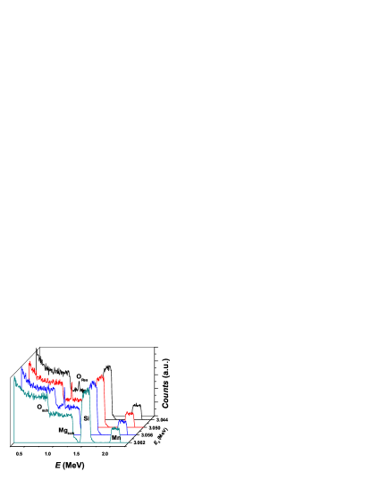
Figure 2 shows RBS spectra for a typical a-MnxSi1-x film (=0.08). Film compositions were obtained from data simulations with error bars of 0.001 and 0.005, for Si and Mn respectively. Oxygen-resonance spectroscopy was used to probe specifically for oxygen contamination (the oxidation enthalpy of Mn is high compared to Si, and would counteract Mn doping and alter the Mn magnetic properties). A He2+ ion beam with O resonance energy (=3.05 MeV) was used and oxygen-resonance RBS peaks (labeled as O in Fig. 2) were observed at 1.1 MeV, indicating a surface oxide layer. By slightly increasing above , oxygen content below the film surface could be probed (the oxygen resonance occurs when the He2+ kinetic energy is reduced to 3.05 MeV after penetrating to a depth below the film surface). If O were observed over a range of , it would indicate oxygen contamination throughout the film. Here, however, the O peak intensity is reduced and eventually disappears after is increased above , as shown in Fig. 2. We can therefore conclude that O is only located near the film surface, within less than a few nm, which is small compared to the total film thickness (400 nm).
The room-temperature (RT) conductivity () of the films as a function of time () after exposure to air from vacuum was monitored and found to be stable up to at least 200 hours. The slightly reduced (4%) for this time period is probably due to a thin self-limiting oxide layer, which is insulating and thus reduces the effective thickness of the film. For this 4% reduction, the estimated thickness of this oxide layer is less than 10 monolayers, in good agreement with the RBS O resonance data reported above.
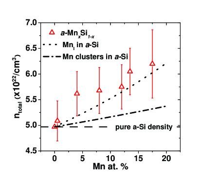
Figure 3 shows the total atomic number density () for different a-MnxSi1-x samples, obtained by dividing the RBS areal density by the film thickness, as measured by atomic force microscopy. Since the structure of high quality a-Si is a continuous random network (CRN), which preserves the local tetrahedral covalent bonding, with small deviations in bond length and bond angle, the for a-Si should still be comparable to that of c-Si Zeng et al. (2007). Undoped a-Si with 98% number density of c-Si is achieved by -beam evaporation Brodsky et al. (1972). In Fig. 3, the of a-MnxSi1-x increases with , as opposed to results in the literature for crystalline c-X1-x:Mnx (XSi, Ge), where additional Mn was found to decrease (i.e. increase the lattice constant) because of lattice strain caused by the larger radius of Mn atoms Cho et al. (2002); Kwon et al. (2005); Ma et al. (2006).
III.2 Conductivity and Magnetization
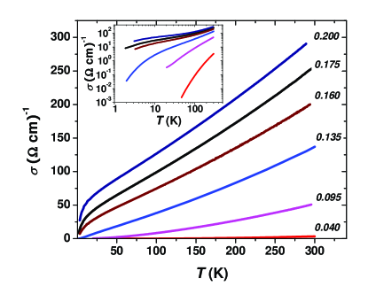
Figure 4 shows the dc conductivity () vs for different . The conductivity has a positive temperature coefficient and increases monotonically with the level of Mn doping, indicating semiconducting behavior and the effect of Mn doping in a-Si. The increasing with increasing is also a signature of localization in a disordered electronic system. A concentration-tuned M-I transition is visible; samples are insulating for 0.135, whereas they are metallic for higher . The 0.135 sample is very close to but slightly on the insulating side. This result is in good agreement with the =0.137 found in Mn-implanted a-Si samples Yakimov and Dvurechenskii (1997).
Magneto-transport properties were measured for one sample on the insulating side (=0.135) and one sample on the metallic side (=0.175). A small positive MR was found down to 2 K at =7 T for both samples, 27% and 16% for =0.135 and =0.175, respectively, which can be attributed to the electron correlation effect in disordered non-magnetic electronic systems Lee and Ramakrishnan (1985). Yakimov and coworkers found a crossover from small positive MR to small negative MR below 2.3 K (-25% at 1.76 K and 4.5 T) for a Mn-ion-implanted a-Si sample (=0.11) held at room temperature for 8 years Yakimov et al. (1995). We did not observe any negative MR in our samples. The negative MR found in Ref. Yakimov et al., 1995 was attributed to magnetic clusters.
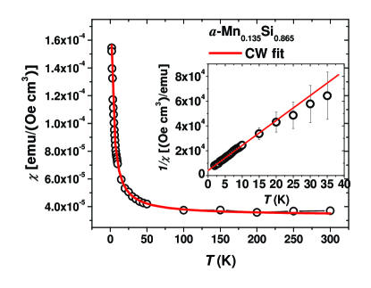
Zero-field-cooled (ZFC) and field-cooled (FC) magnetic susceptibility data were recorded in a dc magnetic field of 1 T. For =0.04, which had the largest raw magnetic signal, ZFC and FC susceptibilities were also measured in smaller fields (= 1000 and 350 Oe). All curves were identical and showed no splitting between ZFC and FC. Measuring at 1 T compared to 350 Oe leads to 10% underestimation of the effective moment (), but it is necessary to obtain reliable magnetic signals from films ( dependent) above the diamagnetic background signal (negligible dependent) for our samples, all of which show very low magnetic signals. The diamagnetic background from the SiNx coated Si substrate was measured for each and , as was an undoped a-Si control sample prepared using the same Si evaporation batch. The resulting net a-MnxSi1-x response followed the Curie-Weiss (CW) law very well with a very low CW temperature (2 K). No ferromagnetic or SG states were observed in the temperature range between 2-40 K. Above 40 K, the error bars were large due to the small signal. The thermoremanent moment (TRM) was obtained by cooling the sample in a field of 7 T and then measuring the TRM on heating the sample in zero magnetic field from 1.9 K to 380 K: no significant signal was obtained at any temperature for any of the samples. These results indicate that the magnetic signal is purely paramagnetic.
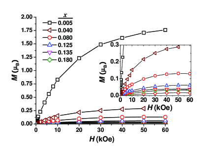
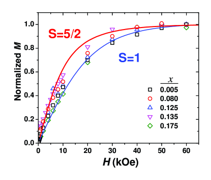
Figure 6 shows (magnetization per Mn atom) vs at 2 K, assuming that all Mn atoms contribute equally to the signal. The diamagnetic background from the substrate was again subtracted. No hysteresis loop was found. decreased very fast with the Mn concentration. If it is assumed that either =1 or 5/2 for =0.005, then 92% or 37% of the Mn atoms are magnetically active, respectively. The vs data for all samples scale well to a Brillouin function for free magnetic ions, as shown in Figure 7. The value of at 6 T should be within 2% of the saturation moment for non-interacting Mn ions (whether =1 or 5/2), and so its value can be used to calculated the saturation moment per Mn atom () as a function of .
IV Discussion
As shown in Fig. 3, the total atomic number density increases with Mn doping. This is comparable to, or slightly higher than, the calculated (also plotted in Fig. 3) assuming all Mn are at interstitial sites without changing the a-Si matrix density, suggesting that Mn atoms act as interstitial dopants in a-MnxSi1-x (therefore are at sites with high Si coordination number and low symmetry). Mn on the other hand would keep constant. The charge and spin states of Mn strongly depend on the local environment. Preliminary ESR results on our films show 2.010.03 for Mn, indicating Mn is in a pure spin state. Based on the LW model proposed for Mn in Si, there are two possible interstitial Mn sites with quenched orbital moment: one is Mn (3, ==5/2) and the other is Mn (3, ==1).
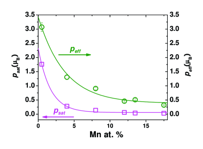
The small magnetization (both and ) of all samples suggests that only a very small fraction of Mn atoms are magnetically active. Based on the saturation moment, we can obtain the fraction of magnetically active Mn ions (denoted as ) assuming ==1 or 5/2. For a pure paramagnetic state, the same magnetic centers contribute to . The atomic moment () and the effective moment () are connected for a specific value, with =2 from ESR data. We re-calculate the new effective moment (now denoted as ) based on (instead of in Fig. 8) and the measured CW constant . For ==1, the resulting values are more than 20% greater than the theoretical value of 2.83 . was determined with a 1 T field, which leads to smaller than determined at lower field, thus underestimating of . This indicates that ==1 is not the correct spin state. For ==5/2, the resulting values are 10% smaller than the theoretical value of 5.92 . We can check the underestimation of by using the Brillouin function for ==5/2 moment at 2 K. Since , the fractional reduction . The calculated from using 1 T instead of the low-field limit is -20%, which gives -10%. Taking this -10% deviation into account, and are in excellent agreement for ==5/2. In Table 1, we summarize all of the fitting parameters as well as the estimated and . The agreement between the atomic moment and the effective moment for all values strongly suggests that Mn (3, ==5/2) are the magnetically active sites in these films, but only account for a small fraction of the total doping (e.g. =0.6% for =0.175).
The decreasing moment seen in Fig. 8 can be explained by as the decrease of with . are 35.2% and 5.6% for the =0.005 and 0.04 films, respectively, and become less than 1% when 0.12 (as shown in Table 1). The rest of the Mn atoms are in a non-magnetic state and contribute to the transport properties only (as shown by the increase of with ).
These two types of Mn states found in a-MnxSi1-x are in sharp contrast to the situation for a-GdxSi1-x, where all Gd atoms are in Gd3+ states, contributing 3 as well as 7 moment (due to the half-filled shell, ==7/2) per Gd. The dual role of Gd is the key to its SG ground state as well as the enormous negative MR in the magnetically doped amorphous semiconductor studied previously Zeng et al. (2007). In a-MnxSi1-x, only a tiny percentage of the Mn sites are magnetically active and therefore far separated, and thus no magnetic interaction is developed as in a-GdxSi1-x. The majority of Mn atoms are in a non-magnetic state (which is not predicted by the LW model), despite contributing to transport. The small positive MR is consistent with this result, as in other non-magnetic disordered systems Lee and Ramakrishnan (1985). We do not observe any negative MR in our co-deposited a-MnxSi1-x films even for samples on the insulating side, as reported previously for Mn-implanted samples Yakimov et al. (1995).
Preliminary X-ray absorption spectroscopy (XAS) data on the Mn and edges for all samples with 0.04 show two peaks with very broad features, quite different from the spectra seen for Mn materials with localized electrons which show distinct multiplets. These broad peaks are evidence that the majority of Mn form an impurity band in the a-Si matrix. States in this band are localized due to disorder when , and delocalized when . Preliminary Hall measurements using lithographically defined Hall patterns suggest an electron-like carrier type for the metallic samples.
How would the amorphous matrix affect the local moment of the Mn sites in a-Si compared to the c-Si case? Mn sites in c-Si do not form covalent bonds with Si and are always predicted to have local moments. This should be the same case in a-Si. However, if any local moment exists in our a-MnxSi1-x films, for the wide concentration and the temperature range measured, one would not expect a purely paramagnetic response with small values and no sign of any magnetic interaction. It is possible but unlikely that local moments exist but are completely canceled because of Mn-Mn AFM interactions, since AFM ordering is not robust to disorder and should lead to a magnetic freezing state, such as a SG phase (with ) or a clustered spin glass (with blocking temperature, ), showing magnetic hysteresis (differences between FC and ZFC states) and TRM. or should increase with the magnetic concentration, but no magnetic freezing was observed for up to 0.175. It is possible that and are so high that samples are already in a frozen state at 40 K and thus only express a very small moment. However, known concentrated SG a-MnSi (1:1 stoichiometry) has a only at 22 K Hauser et al. (1979), while the CW behavior of our samples is reliably measured up to 40 K, as shown in Fig. 5 (above 40 K, the signal is too small with large error bars). of a-MnSi is smaller but comparable to the magnetic ordering temperature (=30 K) of its crystalline counterpart, compound MnSi, which has a helical spin structure with 18 nm wavelength. Above or , in the paramagnetic states, they have comparable , which are 2.2 and 2.6 for the compound MnSi and a-MnSi respectively Cochrane et al. (1979); both of these states would give significantly larger than observed at 40 K.
If there were non-interacting Mn complex clusters in a-Si (invisible in HR-XTEM), such as a Mn-Mn dimer instead of interacting Mn ions, these could be strongly AFM-coupled. Such complexes have not been experimentally observed to the best of our knowledge, and are calculated to be highly unstable energetically Bernardini et al. (2004). Furthermore, only the neutral charge state favors AFM coupling in Si, which should therefore not contribute to the transport. Mn Ludwig and Woodbury (1960) and [Mn-Mn] Kreissl et al. (1994) clusters have large values, thus not the case here. Existence of metallic Mn or Mn-rich clusters of larger scale are not supported by the HR-XTEM results (shown in Fig. 1) and the atomic density analysis (shown in Fig. 3). Moreover, ferromagnetic clusters should result in an enhanced , opposite to what we have seen. All these strongly indicate the majority Mn atoms enter into a non-magnetic doping environment in a-Si, forming even at as low as 0.005 (64.8%).
The totally quenched Mn moment in a-Si is intriguing and needs more understanding. In our two-state scenario, we have argued that the small magnetic signal is due to a small fraction of Mn sites according to the LW model, while the majority of Mn atoms are in a totally non-magnetic state. Based on the comparable (high) atomic number density and the CRN model for a-Si, the local site symmetry should be only slightly perturbed for these Mn when is small, and thus the LW model is still valid at least for low . If adding more Mn enhances the crystal field splitting such that it overrules the LW model and Hund’s rule, a zero moment state could arise (Mn with filled levels, or Mn with filled levels, dependent on which is lower), although such charge states should have multiplets at the edges in XAS measurement due to unfilled levels. Another scenario is itinerant magnetism with very small moment, as found in some Mn silicides, such as the crystalline compound Mn4Si7, where (from CW fit for 40 K, =43 K) and (from saturation at 2 K) were found to be 0.365 and 0.012 respectively Gottlieb et al. (2003). The space group of the tetragonal Mn4Si7 is . The symmetry at the Mn sites in this compound is low and may be a better representation of the local environment of Mn in a-MnxSi1-x. The large / in our samples (as shown in Table 1) may also suggest the existence of itinerant moments Rhodes and Wohlfarth (1963). The existence of itinerant moments in insulating samples is compatible with an Anderson localization model for the effect of strong disorder.
It would be useful to evaluate how disorder affects the charge and spin states of Mn using first-principles calculations. If the analog of the local environment between a-Si and c-Si is valid, and since the local moment is largely determined by the local environment, then Mn would be expected to be in an interstitial site with ==5/2. However, our results indicate almost no moment for Mn, suggesting a new state for Mn in a-Si, which is not predicted by any existing model for Mn in c-Si.
V Conclusion
Magnetic and electrical transport properties were measured for -beam co-deposited homogeneous a-MnxSi1-x with from 0.005 to 0.175. A small fraction of Mn in a Mn configuration account for the small detected paramagnetic signal. The majority of Mn atoms are, however, in a totally non-magnetic state, which is not observed in the crystalline counterpart or predicted by any existing model for transition metal impurities in Si. This explains why MR for a-MnxSi1-x is positive and small, with typical values for disordered non-magnetic electronic systems, unlike a-GdxSi1-x, where an enormous negative MR was measured and explained in terms of interplay between large Gd local moments and charge carriers. The non-magnetic state is most likely due to the formation of an impurity band, subject to localization effects, although a tightly bound dimer state cannot be ruled out.
Acknowledgements.
We thank S. Lofland for ESR data, E. Arenholz, E. Cruz and C. Piamonteze for assistance with XAS experiment, N. Spaldin, A. J. Freeman, Hua Wu and M. Scheffler for useful discussions and D. R. Queen for assistance. We also acknowledge use of facilities in the LeRoy Eyring Center for Solid State Science at Arizona State University. This research was supported by NSF DMR-0505524 and 0203907.References
- Ohno (1998) H. Ohno, Science 281, 951 (1998).
- Dietl et al. (1998) T. Dietl, H. Ohno, F. Matsukura, J. Cibert, and D. Ferrand, Science 287, 1019 (1998).
- Stroppa et al. (2003) A. Stroppa, S. Picozzi, A. Continenza, and A. J. Freeman, Phys. Rev. B 68, 155203 (2003).
- Bernardini et al. (2004) F. Bernardini, S. Picozzi, and A. Continenza, Appl. Phys. Lett. 84, 2289 (2004).
- Weng and Dong (2005) H. Weng and J. Dong, Phys. Rev. B 71, 035201 (2005).
- Weber (1983) E. R. Weber, Appl. Phys. A 30, 1 (1983).
- Park et al. (2002) Y. D. Park, A. T. Hanbicki, S. C. Erwin, C. S. Hellberg, J. M. Sullivan, J. E. Mattson, T. F. Ambrose, A. Wilson, G. Spanos, and B. T. Jonker, Science 295, 651 (2002).
- Kang et al. (2005) J.-S. Kang, G. Kim, S. C. Wi, S. S. Lee, S. Choi, S. Cho, S. W. Han, K. H. Kim, H. J. Song, H. J. Shin, et al., Phys. Rev. Lett. 94, 147202 (2005).
- Kwon et al. (2005) Y. H. Kwon, T. W. Kang, H. Y. Cho, and T. W. Kim, Solid State Commun. 136, 257 (2005).
- Bolduc et al. (2005) M. Bolduc, C. Awo-Affouda, A. Stollenwerk, M. B. Huang, F. G. Ramos, G. Agnello, and V. P. LaBella, Phys. Rev. B 71, 33302 (2005).
- Awo-Affouda et al. (2006) C. Awo-Affouda, M. Bolduc, M. B. Huang, F. Ramos, K. A. Dunn, B. Thiel, G. Agnello, and V. P. LaBella, J. Vac. Sci. Technol. A 24, 1644 (2006).
- Zhou et al. (2007) S. Zhou, K. Potzger, G. Zhang, A. Mücklich, F. Eichhorn, N. Schell, R. Grötzschel, B. Schmidt, W. Skorupa, M. Helm, et al., Phys. Rev. B 75, 085203 (2007).
- Zhang et al. (2005) Y. Zhang, Q. Jiang, D. J. Smith, and J. Drucker, J. Appl. Phys. 98, 033512 (2005).
- Zeng et al. (2007) L. Zeng, E. Helgren, F. Hellman, R. Islam, and D. J. Smith, Phys. Rev. B 75, 184404 (2007).
- Anderson (1961) P. W. Anderson, Phys. Rev. 124, 41 (1961).
- Hertel et al. (1983) G. Hertel, D. J. Bishop, E. G. Spencer, J. M. Rowell, and R. C. Dynes, Phys. Rev. Lett. 50, 743 (1983).
- Teizer et al. (2000a) W. Teizer, F. Hellman, and R. C. Dynes, Solid State Commun. 114, 81 (2000a).
- Teizer et al. (2000b) W. Teizer, F. Hellman, and R. C. Dynes, Phys. Rev. Lett. 85, 848 (2000b).
- Sinenian et al. (2006) N. Sinenian, L. Zeng, E. Helgren, K. McCarthy, J. J. Cherry, F. Hellman, R. Islam, and D. J. Smith, In preparation (2006).
- Helgren et al. (2005) E. Helgren, J. Cherry, L. Zeng, and F. Hellman, Phys. Rev. B 71, 113203 (2005).
- Yakimov et al. (1995) A. I. Yakimov, T. Wright, C. J. Adkins, and A. V. Dvurechenskii, Phys. Rev. B 51, 16549 (1995).
- Yakimov et al. (1997) A. I. Yakimov, A. V. Dvurechenskii, C. J. Adkins, and V. A. Dravin, J. Phys. 9, 499 (1997).
- Yakimov and Dvurechenskii (1997) A. I. Yakimov and A. V. Dvurechenskii, JETP Lett. 65, 354 (1997).
- Ludwig and Woodbury (1960) G. W. Ludwig and H. H. Woodbury, Phys. Rev. Lett. 5, 98 (1960).
- Brodsky et al. (1972) M. H. Brodsky, D. Kaplan, and J. F. Ziegler, Appl. Phys. Lett. 21, 305 (1972).
- Cho et al. (2002) S. Cho, S. Choi, S. C. Hong, Y. Kim, J. B. Ketterson, B.-J. Kim, Y. C. Kim, and J.-H. Jung, Phys. Rev. B 66, 033303 (2002).
- Ma et al. (2006) S. Ma, Y. Sun, B. Zhao, P. Tong, X. Zhu, and W. Song, Solid State Commun. 140, 192 (2006).
- Lee and Ramakrishnan (1985) P. A. Lee and T. V. Ramakrishnan, Rev. Mod. Phys. 57, 287 (1985).
- Hauser et al. (1979) J. J. Hauser, F. S. L. Hsu, G. W. Kammlott, and J. V. Waszczak, Phys. Rev. B 20, 3391 (1979).
- Cochrane et al. (1979) R. W. Cochrane, J. O. Strom-Olsen, and J. P. Rebouillat, J. Appl. Phys. 50, 7348 (1979).
- Kreissl et al. (1994) J. Kreissl, W. Ghlhoff, and H. Vollmer, Phys. Rev. B 49, 10307 (1994).
- Gottlieb et al. (2003) U. Gottlieb, A. Sulpice, B. Lambert-Andron, and O. Laborde, J. Alloys Comp. 361, 13 (2003).
- Rhodes and Wohlfarth (1963) P. Rhodes and E. P. Wohlfarth, Proc.R. Soc. London. A 273, 247 (1963).
| 111From RBS and AFM measurements. | 111From RBS and AFM measurements. | 222 and from CW fit: ; is a small temperature-independent constant due to combined core, and magnetometer background contributions | 222 and from CW fit: ; is a small temperature-independent constant due to combined core, and magnetometer background contributions | 333 per Mn obtained from ; per Mn obtained from saturation moment at 2 K and 6 T, both assuming all contribute equally, with from RBS. | /333 per Mn obtained from ; per Mn obtained from saturation moment at 2 K and 6 T, both assuming all contribute equally, with from RBS. | 444 is the magnetically active Mn concentration obtained from saturation magnetization, assuming each active Mn has ==5/2. | 555 is the calculated effective moment per active Mn atom based on , each with ==5/2. |
| (1021 atoms/cm3) | (K) | (10-4 emu/cmOeK) | () | () | |||
| 0.005 | 0.27 | -1.63 | 5.2 | 3.1 | 1.74 | 5.2 | |
| 0.04 | 2.04 | -0.45 | 7.2 | 1.3 | 4.39 | 5.5 | |
| 0.08 | 4.54 | -1.71 | 7.7 | 0.9 | 6.57 | 5.4 | |
| 0.12 | 6.86 | -0.19 | 3.0 | 0.5 | 7.46 | 4.1 | |
| 0.135 | 8.20 | -1.69 | 4.4 | 0.5 | 13.2 | 5.8 | |
| 0.175 | 10.8 | -1.44 | 2.3 | 0.3 | 9.99 | 4.0 |