Self-assembled Pt nanowires on Ge(001): Relaxation effects
Abstract
Absorption of Pt on the Ge(001) surface results in stable self-organized Pt nanowires, extending over some hundred nanometers. Based on band structure calculations within density functional theory and the generalized gradient approximation, the structural relaxation of the Ge–Pt surface is investigated. The surface reconstruction pattern obtained agrees well with findings from scanning tunneling microscopy. In particular, strong Pt–Pt dimerization is characteristical for the nanowires. The surface electronic structure is significantly perturbed due to Ge–Pt interaction, which induces remarkable shifts of Ge states towards the Fermi energy. As a consequence, the topmost Ge layers are subject to a metal-insulator transition.
pacs:
68.43.Bc, 73.20.-r, 73.20.AtSemiconductor surfaces attract great attention due to a wide field of possible technological application. In particular, for both the Si and the Ge surface various effects of self-organization have been reported in the literature. Self-assembled metallic chains, for example, are formed by Au atoms on Si(553) ahn05 and In atoms on Si(111) hill97 . Electron motion in Ag films grown on these In chains is restricted to the chain direction, giving rise to quantized Ag states nagamura06 . In addition, ultrathin Ag films on Ge(111) are found to be significantly influenced by hybridization between the Ag and Ge surface states tang06 . For Au growth on Ge(001), a large variety of ordering phenomena can be realized as a function of the Au coverage and growth temperature wang0405 . Adsorption of Pt atoms on the Ge(001) surface induces a self-organization of well-ordered chain arrays after high-temperature annealing gurlu03 . Since these nanowires provide a confining potential, interference between Ge(001) surface electrons within the nanowire array comes along with one-dimensional states resembling the energy levels of a quantum particle in a well oncel05 . The spontaneously formed Pt chains are thermodynamically stable, literally defect and kink free, and have lengths up to some hundred nanometers. Using scanning tunneling microscopy, Schäfer et al. schafer06 , however, have shown that their conduction bands are seriously modified by the interaction with the Ge substrate. Exact knowledge about the surface electronic states therefore is mandatory for understanding the self-organization process.
Reconstruction of the clean Ge(001) surface has been subject to extensive investigations, both from the experimental and theoretical point of view zandvliet03 . In particular, neighbouring surface atoms form asymmetric dimers on top of a slightly relaxed substrate, saturating one dangling Ge bond per surface atom. Since these dimers line up along the direction, the surface is well characterized in terms of dimer rows. Further stabilization of the crystal structure can be reached by means of a distinct buckling of the dimers, leading to specific reconstruction patterns with respect to the realized buckling directions. In particular, the room temperature configuration transforms into a structure at low temperature, where the order-disorder phase transition is accompanied by a surface metal-insulator transition. Scanning tunneling spectroscopy entails that subtleties of the reconstruction pattern seriously affect the Ge(001) surface states gurlu04 . Nevertheless, when the structural relaxation is carried out carefully, band structure calculations have shown the capability to perfectly reproduce the experimental surface density of states (DOS) prb07 .

A comparative study of the surface reconstructions of diamond, Si, and Ge has been reported by Krüger and Pollmann kruger95 , including a comprehensive review on previous ab initio calculations. While for diamond a symmetric dimer configuration is established, asymmetric ordering leads to an energy gain of about 0.1 eV per dimer in the cases of Si and Ge. The dimer formation on adsorption of In on Ge(001) has been analyzed by Çakmak and Srivastava cakmak04 via first principles total energy calculations. Their data stress the importance of the very details of the surface electronic structure for the adsorption mechanism. Expectedly, this likewise applies to the adsorption of other atoms and molecules, such as alkali metals xiao06 or GeH4 cocoletzi05 , for instance.
Because self-organization of adsorpted atoms relys on strong interaction with surface states, accounting for the full structural relaxation is a prerequisite for describing the electronic properties of a covered surface in an adequate manner. In a first step, the present work therefore aims at clarifying the reconstruction pattern induced by self-assembled Pt chains on the Ge(001) surface. Afterwards, we show that the original Ge(001) surface states are subject to strong modifications due to Ge–Pt interaction, giving rise to a transition into a metallic regime.
Our first principles calculations are based on a supercell of the cubic Ge unit cell consisting of one reconstructed surface array and extending two unit cells perdendicular to the surface. With respect to the parent diamond lattice, our tetragonal supercell thus is given by the lattice vectors , , and . X-ray diffraction data of Ferrer et al. ferrer95 and first principles data of Yoshimoto et al. yoshimoto00 can be used for starting the structure optimization, which we first carry out for the clean Ge(001) surface without Pt chains. Here and in the following, we apply the generalized gradient approximation within density functional theory, as implemented in the WIEN2k package wien2k . This full-potential linearized augmented plane wave code has shown great capability in dealing with structural relaxation at surfaces and interfaces uscs1 ; uscs2 . In particular, the exchange-correlation potential is parametrized according to the Perdew-Burke-Ernzerhof scheme. We assume convergence of the relaxation when all the surface forces have decayed, i.e. have reached values below a threshold of 5 mRyd/. To have reliable results, we represent the charge density by some 460,000 plane waves and use for the Brillouin zone integrations a k-mesh comprising 12 points in the irreducible wedge. While Ge and Pt , orbitals are treated as semi-core states, the valence states consist of Ge , , and Pt , , , orbitals. We have checked convergence of the band structure results with respect to the thickness of the Ge slab applied in the calculation.
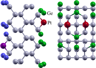
According to scanning tunneling microscopy data by Gurlu et al. gurlu03 , the formation of Pt chains on Ge(001) is accompanied by the partial breakup of the Ge surface dimers. These authors have obtained nanowires only on Pt modified Ge(001) terraces with mixed Ge–Ge and Ge–Pt dimers. However, as it cannot be excluded that they likewise can be grown on a pure Ge surface, we have investigated self-assemblance on the pure and the Pt modified Ge(001) surface. Because we find qualitatively the same behaviour in both cases, we subsequently focuss on the pure Ge surface, in order to clearly resolve the effects of Ge–Pt hybridization under Pt adsorption. To be more specific, the reconstructed Ge(001) surface consists of Ge troughs, which can accommodate the nanowires, see the left hand side projection (along the -axis) of the crystal structure in Fig. 1. Due to the occupation of trough sites by Pt atoms, the upper Ge dimer sites stay unoccupied on one side of the nanowire, which is illustrated in Fig. 1 by a projection perpendicular to the surface (along the -axis). Since only every second Ge trough is occupied, the distance between neighbouring nanowires along the -axis amounts to almost exactly 16 Å. For obtaining a reasonable starting point for the structure optimization of the Pt covered Ge(001) surface, we thus use the unit cell of the clean Ge surface, leave away every fourth row of upper Ge dimer sites and place Pt sites in the trough next to this row. As suggested by gurlu03 , we assume the Pt atoms to be located in the middle of the troughs (along the -axis) and the Pt–Pt bond lengths to resemble the distance of adjacant Ge dimers along the row direction. With respect to the dimer rows, the Pt chain is shifted by half that distance along the -axis, see Fig. 1.
Applying this structure model, surface forces decayed quickly during the structure optimization. While the Pt sites are subject to strong relaxation, shifts of Ge sites are small, see Table 1. The lower dimer sites next to the Pt chain move off the chain axis by 0.05 Å, whereas the remaining upper dimer sites approach it by 0.05 Å. Only minor shifts are found both perpendicular to the surface and in the chain direction. In contrast, the nanowire develops strong dimerization with alternating Pt–Pt bond lengths of 3.50 Å and 4.50 Å, confirming the experiments of Gurlu et al. gurlu03 . As a consequence, the bond length to the nearest upper dimer Ge site decreases to 2.97 Å and the distance to the nearest lower dimer Ge site grows to 3.83 Å. The shortest Ge–Pt bond lengths of 2.41 Å and 2.44 Å appear within the Ge troughs. Since the Pt chain is not subject to buckling perpendicular to its axis, the Pt–Pt bond angle maintains a value of almost 180∘. For convenience, important bond lengths for the relaxed Ge–Pt surface are summarized in Table 2.
| -axis | -axis | -axis | |
|---|---|---|---|
| upper dimer Ge (full row) | Å | Å | Å |
| lower dimer Ge (full row) | Å | Å | Å |
| lower dimer Ge (partial row) | Å | Å | Å |
| bond length | |
|---|---|
| upper dimer Ge – Pt | 2.97 Å |
| lower dimer Ge – Pt | 3.83 Å |
| trough Ge – Pt | 2.41 Å, 2.44 Å |
| Pt – Pt (along -axis) | 16.0 Å |
| Pt – Pt (along -axis) | 3.50 Å, 4.50 Å |
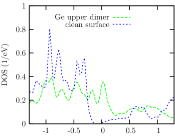
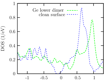
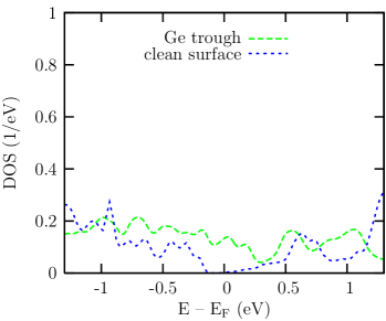
Having clarified the structural details of the Pt covered Ge(001) surface, we now turn to the relaxation effects on the Ge surface states. Fig. 2 compares partial Ge densities of states (DOS) as resulting from our band structure calculation for the relaxed Ge–Pt surface to data of the clean reconstructed surface prb07 . The three panels shown refer to three characteristic atomic sites: the upper and lower dimer site as well as a typical trough site. For the clean surface, electronic states tracing back to the upper Ge dimer atom are found mainly below the Fermi level. In contrast, the DOS of the lower Ge dimer atom has its maximum above the Fermi level, which reflects a remarkable amount of charge transfer from the lower to the upper dimer site. Importantly, for all Ge sites spectral weight is missing at the Fermi energy, which agrees perfectly with the prediction of an insulating surface state, see gurlu04 and the references in this paper.


Accounting for the Pt chains, the shapes of the DOS curves in Fig. 2 change dramatically. For the upper Ge dimer site, weight is lost at energies below eV and reappears near the Fermi energy, hence closing the insulating energy gap. Alterations of the unoccupied states are much less pronounced. For the lower Ge dimer site, the situation is virtually inverted. While strong changes affect the unoccupied states, again shifting weight to the Fermi energy, the occupied states mainly maintain their original shape. In a first step, we interpret these facts in terms of perturbed Ge–Ge dimer bonds. Charge transfer from the lower to the upper dimer atom, in principle, results in a filled Dup and an empty Ddown surface band, which opens the energy gap. Due to surface strain induced by the Pt chains, the Ge dimers are forced to give up their ideal geometry and charge transfer is reduced as a consequence. The Dup band hence is partially depleted while the Ddown band is filled accordingly. In addition to the variation of the dimer bonds, the surface states likewise are influenced by strong hybridization with the Pt conduction bands. This becomes obvious on inspection of the trough Ge atoms, which are not involved in dimer bonding, see the bottom panel of Fig. 2. In the energy range from eV to 0.3 eV the DOS grows seriously for the Pt covered surface, particularly inducing a metallic state. Since each of the surface Ge atoms is observed to develop conduction states, the coaction of structural relaxation and Ge–Pt hybridization effectively causes an metal-insulator transition of the entire surface.
In conclusion, we have studied the relaxation and electronic structure of the reconstructed Ge(001) surface covered with self-organized Pt nanowires. The surface geometry and electronic states have been discussed using results from band structure calculations based on density functional theory. We have carefully analyzed the surface reconstruction pattern induced by adsorption of Pt atoms, confirming a strong tendency towards Pt–Pt dimerization with intrachain bond lengths of 3.50 Å and 4.50 Å. In addition, we have succeeded in establishing a comprehensive structure model for a Pt covered Ge(001) surface. By a fully relaxed crystal structure, alterations of the Ge surface states due to interaction with the Pt chains could be investigated. Our results are evident as concerns the existence of a surface phase transition into a metallic state. We attribute this transition to two cooperative effects: (1) A shift of surface Ge states towards the Fermi energy due to a modified bonding within the Ge dimers and (2) considerable hybridization of the Ge states and the metallic Pt states. The metallicity of the topmost Ge layers is expected to significantly affect the transport properties of the Pt nanowires. Moreover, the observed interplay between a strong Pt–Pt dimerization and Ge–Pt hybridization agrees well with the data of recent experiments by scanning tunneling microscopy schafer06 .
Acknowledgement
We thank U. Eckern and V. Eyert for helpfull discussions, and the Deutsche Forschungsgemeinschaft for financial support (SFB 484).
References
- (1) J.R. Ahn, P.G. Kang, K.D. Ryang, and H.W. Yeom, Phys. Rev. Lett. 95, 196402 (2005).
- (2) I.G. Hill and A.B. McLean, Phys. Rev. B 56, 15725 (1997).
- (3) N. Nagamura, I. Matsuda, N. Miyata, T. Hirahara, S. Hasegawa, and T. Uchihashi, Phys. Rev. Lett. 96, 256801 (2006).
- (4) S.-J. Tang, T. Miller, and T.-C. Chiang, Phys. Rev. Lett. 96, 036802 (2006).
- (5) J. Wang, M. Li, and E.I. Altman, Phys. Rev. B 70, 233312 (2004); Surf. Sci. 596, 126 (2005).
- (6) O. Gurlu, O.A.O. Adam, H.J.W. Zandvliet, and B. Poelsema, Appl. Phys. Lett. 83, 4610 (2003).
- (7) N. Oncel, A. van Houselt, J. Huijben, A.-S. Hallbäck, O. Gurlu, H.J.W. Zandvliet, and B. Poelsema, Phys. Rev. Lett. 95, 116801 (2005).
- (8) J. Schäfer, D. Schrupp, M. Preisinger, and R. Claessen, Phys. Rev. B 74, 041404(R) (2006).
- (9) H.J.W. Zandvliet, Phys. Rep. 388, 1 (2003).
- (10) O. Gurlu, H.J.W. Zandvliet, and B. Poelsema, Phys. Rev. Lett. 93, 066101 (2004).
- (11) U. Schwingenschlögl and C. Schuster, Chem. Phys. Lett., in press.
- (12) P. Krüger and J. Pollmann, Phys. Rev. Lett. 74, 1155 (1995).
- (13) M. Çakmak and G.P. Srivastava, Surf. Sci. 566, 931 (2004).
- (14) H.Y. Xiao, X.T. Zu, Y.F. Zhang, and F. Gao, Chem. Phys. Lett. 417, 6 (2006).
- (15) G.H. Cocoletzi, P.H. Hernández, and N. Takeuchi, Thin Sol. Films 490, 196 (2005).
- (16) S. Ferrer, X. Torrelles, V.H. Etgens, H.A. van der Vegt, and P. Fajardo, Phys. Rev. Lett. 75, 1771 (1995).
- (17) Y. Yoshimoto, Y. Nakamura, H. Kawai, M. Tsukada, and M. Nakayama, Phys. Rev. B 61, 1965 (2000).
- (18) P. Blaha, K. Schwarz, G. Madsen, D. Kvasicka, and J. Luitz, WIEN2k: An augmented plane wave and local orbitals program for calculating crystal properties (Vienna University of Technology, Austria, 2001).
- (19) U. Schwingenschlögl and C. Schuster, Chem. Phys. Lett. 435, 100 (2007); Chem. Phys. Lett. 439, 143 (2007).
- (20) U. Schwingenschlögl and C. Schuster, Europhys. Lett. 77, 37007 (2007); Appl. Phys. Lett. 90, 192502 (2007).