Bipolar Spintronics: From spin injection to spin-controlled logic
Abstract
An impressive success of spintronic applications has been typically realized in metal-based structures which utilize magnetoresistive effects for substantial improvements in the performance of computer hard drives and magnetic random access memories. Correspondingly, the theoretical understanding of spin-polarized transport is usually limited to a metallic regime in a linear response, which, while providing a good description for data storage and magnetic memory devices, is not sufficient for signal processing and digital logic. In contrast, much less is known about possible applications of semiconductor-based spintronics and spin-polarized transport in related structures which could utilize strong intrinsic nonlinearities in current-voltage characteristics to implement spin-based logic. Here we discuss the challenges for realizing a particular class of structures in semiconductor spintronics: our proposal for bipolar spintronic devices in which carriers of both polarities (electrons and holes) contribute to spin-charge coupling. We formulate the theoretical framework for bipolar spin-polarized transport, and describe several novel effects in two- and three-terminal structures which arise from the interplay between nonequilibrium spin and equilibrium magnetization.
.1 1. Introduction
In contrast to well-established applications based on metallic magnetic multilayers Maekawa (2006) (Ed.); Maekawa and T. Shinjo (2002) (Eds.); Parkin et al. (2003); Prinz (1998); Ansermet (1998); Hartman (2000) (Ed.); Hirota et al. (2002); Gregg et al. (1997); Johnson (1994); Moodera and Mathon (1999); Parkin et al. (1999); Tehrani et al. (2000); Johnson (2001); Žutić et al. (2004), much less is known about the prospect for utilizing semiconductors in spintronic applications. Typically, these commercial metal-based applications rely on magnetoresistive effects and employ two-terminal structures known as the spin-valves in which a nonmagnetic material is sandwiched between two ferromagnetic electrodes. The flow of carriers through a spin-valve is determined by the direction of their spin (up or down) relative to the magnetization of the device’s electrodes leading thus to magnetoresistance. Since magnetization in ferromagnets persists even when the power is switched off, these applications have significant advantage of being nonvolatile. However, for advanced functions, such as signal processing and digital logic, two-terminal devices such as those are of limited use. Spin logic will also require three-terminal devices and could benefit from incorporating semiconductors with their intrinsic nonlinear current-voltage characteristics, suitable for signal amplification.
An early proposal for a semiconductor-based spin-logic device is the Datta-Das spin field effect transistor (FET) Datta and Das (1990), depicted in Fig. 1. While, despite the extensive experimental efforts, there remain important challenges for its realization Žutić et al. (2004), it is helpful to illustrate a generic scheme for a spin logic device with basic elements such as spin injection and detection as well as spin transport and manipulation.
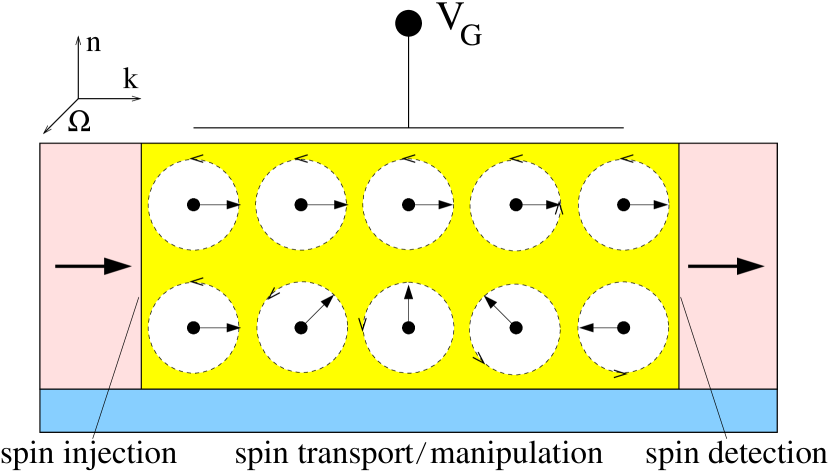
The spin FET, which can be viewed as gate-controlled (via spin-orbit coupling) spin-valve, has also spurred many related transistor schemes Wang et al. (2003); Schliemann et al. (2003); Matsuyama et al. (2002); Mirales and Kirczenow (2001); Ciuti et al. (2002); Nikonov and Bourianoff (2005); Sugahara and Tanaka (2004, 2005); Žutić et al. (2004) . However, a similar functionality has been recently realized in a very different implementation using a carbon nanotube (CNT), rather than a semiconductor Schäpers et al. (2001), as the nonmagnetic material sandwiched between the ferromagnetic source and drain with tunneling contacts. While a CNT has a negligible spin-orbit coupling, the tunability of both the magnitude and the sign of tunneling magnetoresistance in such a CNT spin-valve was controlled by gate voltage which changed on or off-resonance condition Sahoo et al. (2005); Žutić and Fuhrer (2005). Another interesting feature of the Datta-Das spin FET is that it shows the importance of magnetic heterojunctions as the building block for various semiconductor spin-based devices. In this article we will review a theory for bipolar spin-polarized transport in magnetic semiconductor heterojunctions and show possible implications for spin injection and spin-controlled logic. The term bipolar indicates that carriers of both polarities (electrons and holes) are important bip . In contrast to unipolar devices, such as metallic spintronic devices Maekawa et al. (2002); Parkin et al. (2003), bipolar devices exhibit large deviations from local charge neutrality and intrinsic nonlinearities in the current-voltage characteristics, which are important even at small applied bias.
These characteristics, together with the ease of manipulating the minority charge carriers, enable the design of active devices that can amplify signals—as well as provide additional degrees of control not available in charge-based electronics. Analogous to the bipolar charge-transport Shockley (1950); Sze (1981) which is dominated by the influence of the nonequilibrium carrier density, the nonequilibrium spin density (unequal population of “spin up” and “spin down” carriers) plays an important role in bipolar spintronics. A spin light emitting diode (LED), depicted in Fig. 2 can be viewed as a prototypical bipolar spintronic device. Similar to a an ordinary LED Sze (1981), electrons and holes recombine (in a quantum well or a p-n junction) and produce electroluminescence. However, in a spin LED, as a consequence of radiative recombination of spin-polarized carriers, the emitted light is circularly polarized and could be used to trace back the degree of polarization of carrier density upon injection into a semiconductor. While spin LEDs may not be directly lead to spin logic, they have been widely used as detectors for spin polarization, injected optically or electrically into a semiconductor Fiederling et al. (1999); Jonker et al. (2000); Young et al. (2002); Hanbicki et al. (2003); Jiang et al. (2003); Van Roy et al. (2006).

Another important structure for bipolar spintronics is a semiconductor-based magnetic heterojunction and its special cases such as p-n junctions. In addition to being elements of spin FETs and spin LEDs, as we shall show, they are also the building blocks for bipolar devices which could enable a spin-controlled logic. Early experimental efforts date back to nearly 40 years ago. It was shown that a ferromagnetic p-n junction, based on the ferromagnetic semiconductor CdCr2Se4 doped with Ag acceptors and In donors, could act as a diode. Photo-voltaic diodes were also fabricated using (Hg,Mn)Te magnetic semiconductor Janik and Karczewski (1988). However, a more extensive work on magnetic p-n junction have begun after the discovery of (III,Mn)V ferromagnetic semiconductors such as (In,Mn)As Munekata et al. (1989); Ohno et al. (1992); Munekata et al. (1991), and (Ga,Mn)As Ohno et al. (1996); Van Esch et al. (1997); Hayashi et al. (1997), reviewed in Refs. Ohno (1998); Dietl (2002); Jungwirth et al. (2006). Heavily doped -(Ga,Mn)As/-GaAs junctions were fabricated Ohno et al. (2000a); Kohda et al. (2001); Johnston-Halperin et al. (2002); Arata et al. (2001); Van Dorpe et al. (2004), to demonstrate tunneling interband spin injection. Furthermore, it was shown that the current in -CoMnGe/-Ge magnetic heterojunction diodes can indeed be controlled by magnetic field Tsui et al. (2003).
Potentially valuable property for all-semiconductor device designs is the external control of Curie temperature (). Carrier-mediated ferromagnetism in dilute magnetic semiconductors such as (In,Mn)As, (Ga,Mn)As, and MnGe Ohno (1998); Dietl (2003); Samarth et al. (2003); Park et al. (2002); Li et al. (2005) allows for tuning the strength of the ferromagnetic interactions and, therefore, . For example, when the number of carriers is changed, either by shining light Koshihara et al. (1997); Oiwa et al. (2002) or by applying a gate bias in a field effect transistor geometry Ohno et al. (2000b), the material can be switched between the paramagnetic and ferromagnetic states. These experiments suggest the prospect of nonvolatile multifunctional devices with tunable optical, electrical, and magnetic properties. Furthermore, the demonstration of optically or electrically controlled ferromagnetism provides a method for distinguishing carrier-induced semiconductor ferromagnetism from ferromagnetism that originates from metallic magnetic inclusions De Boeck et al. (1996).
An important challenge for potential spin logic applications is the demonstration of room temperature operations. In all-semiconductor schemes it would be desirable to have ferromagnetic materials with high . Some of the promising developments include (Ga,Mn)As with K Nazmul et al. (2005) and (Zn,Cr)Te with K Saito et al. (2003). However, there is a wide range of other materials with much higher predicted and/or reported Dietl (2002); Pearton et al. (2003); Erwin and Žutić (2004) which need to be critically examined and their potential tested in the actual device structures.
An alternative route to room temperature operation is the use of hybrid structures that combine metallic ferromagnets with high and semiconductors. It is important to note that in such systems tailoring of interfacial properties can significantly improve magnetoresistive effects or spin injection efficiency Rashba (2000); Smith and Silver (2001); Fert and Jaffres (2001); Zega et al. (2006). For example, a use of MgO (instead of Al2O3) as a tunnel barrier between CoFe electrodes in a magnetic tunnel junction can lead to a dramatic increase in room temperature tunneling magnetoresistance Parkin et al. (2004); Yuasa et al. (2004), confirming previous theoretical predictions Butler et al. (2001); Mathon and Umerski (2001). Furthermore, it was demonstrated that employing a CoFe/MgO tunnel injector can provide robust room temperature spin injection in semiconductors such as GaAs Jiang et al. (2005); Wang et al. (2005) with room temperature spin polarization of injected electrons exceeding 70 % Salis et al. (2005).
We first formulate drift-diffusion equations for bipolar spin-polarized transport. Next we consider spin injection and extraction in magnetic p-n junction as well as an interplay between equilibrium magnetization and the injected nonequilibrium spin which leads to a strong spin-charge coupling. In the last section we review the basics of bipolar junction transistor and our proposal for its generalization–the magnetic bipolar transistor.
.2 2. Bipolar Spin-Polarized Transport
.2.1 2.1 Spin-polarized drift-diffusion equations
Spin-polarized bipolar transport can be thought of as a generalization of its unipolar counterpart. Specifically, a spin-polarized unipolar transport, in a metallic regime, can then be obtained as a limiting case by setting the electron-hole recombination rate to zero and considering only one type of carriers (either electrons or holes). In the absence of any spin polarization, equations which aim to describe spin-polarized bipolar transport need to recover a description of charge transport. A conventional charge transport in semiconductors is often accompanied with large deviations from local charge neutrality (for example, due to materials inhomogeneities, interfaces, and surfaces) and Poisson’s equation needs to be explicitly included. If we consider (generally inhomogeneous) doping with density of ionized acceptors and donors we can then write
| (1) |
were , (electron and hole densities) also depend on the electrostatic potential and permittivity can be spatially dependent. In contrast to the metallic regime, even equilibrium carrier density can have large spatial variations which can be routinely tailored by the appropriate choice of the doping profile []. Furthermore, charge transport in semiconductors can display strong nonlinearities, for example, exponential-like current-voltage dependence of a diode Sze (1981).
We briefly recall here a case of a unipolar spin-polarized transport in a metallic regime. The basic theoretical understanding dates back to Mott Mott (1936). He noted that the electrical current in ferromagnets could be expressed as the sum of two independent and unequal parts for two different spin projections implying that the current is spin polarized. We label spin-resolved quantities by or for spin up, or for spin down along the chosen quantization axis. For a free electron, spin angular momentum and magnetic moment are in opposite directions, and what precisely is denoted by “spin up” varies in the literature Jonker et al. (2004). Conventionally, in metallic systems Gijs and Bauer (1997), spin up refers to carriers with majority spin. This means that the spin (angular momentum) of such carriers is antiparallel to the magnetization. Some care is needed with the terminology used for semiconductors, the terms majority and minority there refer to the relative population of charge carriers (electrons or holes). Spin-resolved charge current (density) in a diffusive regime can be expressed as
| (2) |
where is conductivity and the chemical potential (sometimes also referred to as the electrochemical potential) is
| (3) |
with proton charge, diffusion coefficient, the change of electron density from the equilibrium value for spin , and the electric potential. We use a notation in which a general quantity is expressed as sum of equilibrium and nonequilibrium parts . Here we focus on the case of a collinear magnetization. More generally, for a noncollinear magnetization, becomes a second-rank tensor Johnson and Silsbee (1988); Stiles and Zangwill (2002).
In the steady state the continuity equation is
| (4) |
and is the average time for flipping a -spin to -spin. For a degenerate conductor the Einstein relation is
| (5) |
where and is the density of states. Using a detailed balance Hershfield and Zhao (1997) together with Eqs. (3) and (5), the continuity equation can be expressed as Rashba (2002); Takahashi and Maekawa (2003)
| (6) |
where is the spin relaxation time. Equation (6) implies the conservation of charge current , while the spin counterpart, the difference of the spin-polarized currents is position dependent.
Following the work of Mott, a unipolar spin-polarized transport and spin injection in the metallic regime is usually described using equivalent resistor schemes with two resistors of different magnitudes, one for each spin direction, also known as the “two-current model” Žutić et al. (2004); Jonker et al. (2003); Jedema et al. (2001); Valet and Fert (1993). This approach implies a linear response in which injected spin polarization and assumes that there are no interfacial spin-flip processes. However, the latter assumption, widely used since the first demonstration of spin injection in metals Johnson and Silsbee (1985), may need to be reconsidered Rashba (2002) when analyzing room temperature spin injection experiments Garzon et al. (2005); Godfrey and Johnson (2006).
Returning to the case of spin-polarized transport in semiconductors, we formulate a drift-diffusion model which will generalize the considerations of Eq. (2)–(6) to include both electrons and holes Žutić et al. (2001a, 2002); Fabian et al. (2002a). We recall that from Eqs. (2) and (3) spin-resolved current have a drift part (proportional to electric field i.e., ) and a diffusive part (), which we want to extend to also capture the effects of band bending, band offsets, various materials inhomogeneities, and the presence of two type of charge carriers. For nondegenerate doping levels (Boltzmann statistics) the spin-resolved components are
| (7) |
where subscripts and label quantities which pertain to the conduction and valence bands. For example, are effective density of states with the corresponding effective masses and is the Boltzmann constant. From the total electron density and the spin density we can define the spin polarization of electron density as
| (8) |
Such a finite spin polarization does not necessarily require ferromagnetic materials or external magnetic fields at all. For example, circularly polarized light provides an effective way to generate net spin polarization in direct-band-gap semiconductors. The angular momentum of the absorbed light is transferred to the medium; this leads directly to orientation of the electron orbital momenta and, through spin-orbit interaction, to polarization of the electron spins Meier and Zakharchenya (1984) (Eds.). In bulk III-V semiconductors, such as GaAs, optical orientation can lead to 50% polarization of the electrons; this can be further enhanced by using quantum structures of reduced dimensionality, or by applying strain.
We consider a general case where the spin splitting of conduction and valence band, expressed as and , can be spatially inhomogeneous Žutić et al. (2002). Splitting of carrier bands (Zeeman or exchange) can arise due to doping with magnetic impurities and/or applied magnetic field. The spin- conduction band edge (see Fig. 3)
| (9) |
differs from the corresponding nonmagnetic bulk value due to electrostatic potential and the spin splitting . The discontinuity of the conduction band edge is denoted by . In the nonequilibrium state a chemical potential for -electrons is and generally differs from the corresponding quantity for holes. While has an analogous role as electrochemical potential in Eqs. (2) and (3), following the conventional semiconductor terminology, we refer to it here as the chemical potential, which is also known as the quasi-Fermi level. An analogous notation holds for the valence band and holes. For example, in Eq. (7) is the spin- density of holes with .

By assuming the drift-diffusion dominated transport across a heterojunction, the spin-resolved charge current densities can be expressed as Žutić et al. (2006a)
| (10) | |||||
| (11) |
where and are mobility and diffusion coefficients (we use symbol to distinguish it from chemical potential ). We note that “drift terms” have quasi-electric fields that are generally spin-dependent ( is referred to as a magnetic drift Žutić et al. (2002)) and different for conduction and valence bands. In contrast to homojunctions, additional “diffusive terms” arise due to the spatial dependence of , and therefore of . In nondegenerate semiconductors and are related by Einstein’s relation
| (12) |
which differs from the metallic (completely degenerate) case given by Eq. (5).
With two type of carriers the continuity equations are more complex than those in metallic systems. After including additional terms for recombination of electrons and holes as well as photoexcitation of electron-hole pairs, we can write these equations as
Generation and recombination of electrons and holes of spin can be characterized by the rate coefficient , the spin relaxation time for electrons and holes is dented by and the photoexcitation rate represents the effects of electron-hole pair generation and optical orientation. Spin relaxation equilibrates carrier spin while preserving nonequilibrium carrier density and for nondegenerate semiconductors , where from Eq. (7) an equilibrium polarization of electron density is
| (15) |
and an analogous expression holds for holes and .
The system of drift-diffusion equations (Poisson and continuity equations) can be self-consistently solved numerically Žutić et al. (2001a, b, 2002) and under simplifying assumptions (similar to the case of charge transport) analytically Fabian et al. (2002a); Žutić et al. (2003, 2006a). Heterojunctions, such as one sketched in Fig. 3, can be thought of as building blocks of bipolar spintronics. To obtain a self-consistent solution in such a geometry, only the boundary conditions at and need to be specified. On the other hand, for an analytical solution we also need to specify the matching conditions at and , the two edges of the space charge region (or depletion region), in which there is a large deviation from the local charge neutrality, accompanied by a band bending and strong built-in electric field.
We illustrate how the matching conditions for spin and carrier density can be applied within the small-bias or low-injection approximation, widely used to obtain analytical results for charge transport Sze (1981); Ashcroft and Mermin (1976). In this case nonequilibrium carrier densities are small compared to the density of majority carriers in the corresponding semiconductor region. For materials such as GaAs a small bias approximation gives a good agreement with the full self-consistent solution up to approximately 1 V Žutić et al. (2001b, 2002). To simplify our notation, we consider a model where only electrons are spin polarized (), while it is straightforward to also include spin-polarized holes Žutić et al. (2006a); Fabian et al. (2002a). Outside the depletion charge region materials parameters (such as, , , , , , and ) are taken to be constant. The voltage drop is confined to the depletion region which is highly resistive and depleted from carriers. In thermal equilibrium the built-in voltage can be simply evaluated from Eq. (7) as
| (16) |
while the applied bias (taken to be positive for forward bias) can be expressed as
| (17) |
implying that the total junction potential between and is . For a heterojunction sketched in Fig. 3 the width of a depletion (space-charge) region is
| (18) |
where the built-in voltage is . Outside of the depletion region the system of drift-diffusion equations reduces usually to only diffusion equations for spin density and the density of minority carriers, while the density of majority carriers are simply given by the density of donors and acceptors Žutić et al. (2002); Fabian et al. (2002a). These diffusion equations contain spin and charge diffusion lengths
| (19) |
in which would provide a characteristic lengthscale for the spatial decay of nonequilibrium spin or charge by substituting for the appropriate (electron or hole) diffusion coefficient and for (spin or charge) the characteristic timescale. However, there are situations, due to additional effects of spin-orbit coupling or simultaneous spin polarization of electrons and holes in magnetic semiconductors, in which diffusion equations become more complicated and Eq. 19 needs to be generalized Tse et al. (2005); Žutić et al. (2006a). For several decades the techniques of optical orientation have been used to directly measure the characteristic timescale for the decay of nonequilibrium electron spin Meier and Zakharchenya (1984) (Eds.) reaching up to 30 ns Weisbuch (1977). More recent optical measurements have shown at low temperatures even longer spin lifetime in GaAs ( ns) Dzhioev et al. (1997) and ( ns) Kikkawa and Awschalom (1998); Dzhioev et al. (2001) which could reach ns at room temperature. Spin-orbit coupling in the valence band typically leads to much faster spin relaxation of holes than electrons (spin lifetimes are 3-4 orders of magnitude shorter in GaAs at room temperature Hilton and Tang (2002)) further supporting our approximation of spin-unpolarized holes. The related issues of spin relaxation and spin dephasing in GaAs have been extensively reviewed in Ref. Žutić et al., 2004.
From Eq. (7) we rewrite electron density by separating various quantities into equilibrium and nonequilibrium parts as
| (20) |
and electron carrier and spin density (for simplicity we omit subscript ”” when writing ) can be expressed as Fabian et al. (2002a)
| (21) |
| (22) |
where , and the polarization of electron density is
| (23) |
If we assume that the spin-resolved chemical potentials are constant for [which means that the depletion region is sufficiently narrow so that the spin relaxation and carrier recombination can be neglected there] it follows, from Eq. (23) and , that
| (24) |
where (left) and (right) label the edges of the space-charge (depletion) region of a p-n junction. Correspondingly, represents the nonequilibrium electron polarization, evaluated at , arising from a spin source. For a homogeneous equilibrium magnetization (), ; the nonequilibrium spin polarization is the same across the depletion region. Equation (24) demonstrates that only nonequilibrium spin, already present in the bulk region, can be transferred through the depletion region at small biases Žutić et al. (2001a, 2002); Fabian et al. (2002a).
Our assumption of constant spin-resolved chemical potentials is a generalization of a conventional models for charge transport in which both and are assumed to be constant across the depletion region Ashcroft and Mermin (1976). From Eqs. (17), (21), and (22) we can obtain minority carrier and spin densities at
| (25) |
| (26) |
which in the absence of nonequilibrium spin () reduce to the well-known Shockley relation for the minority carrier density at the depletion region Shockley (1950)
| (27) |
and an analogous formula holds for spin
| (28) |
.2.2 2.2 Magnetic p-n junctions
Even in nonmagnetic p-n junctions the presence of nonequilibrium spin (created electrically or optically) can have interesting implications. By the term nonmagnetic we imply the limit of vanishing equilibrium magnetization or, equivalently, vanishing spin polarization since . We have predicted that the nonequilibrium spin polarization is bias dependent. By analogy with junction capacitance, this effect could be called spin-capacitance as the amount of accumulated spin changes with applied bias. In contrast to the usual monotonic spatial decay of spin density in the nonmagnetic metal Žutić et al. (2004), away from the point of spin injection, in inhomogeneously doped semiconductors (such as p-n junctions) the spatial profile can be qualitatively different. Spin density can even increase inside the nonmagnetic region, away from the point of spin injection, which we refer to as (spatial) spin density amplification Žutić et al. (2001a, 2006b). Illumination of p-n junction by circularly polarized light can lead to spin electromotive force (EMF) to generate spin-polarized currents even at no applied bias and to provide an open-circuit voltage. In addition to our proposal for a p-n junction-based spin-polarized solar battery Žutić et al. (2001b), there is a range of other structures which could be used as a source of spin EMF Ganichev and Prettl (2003); Long et al. (2003); Mal’shukov et al. (2003) or which could display the effects of spin capacitance Datta (2005) and spatial spin amplification Ganichev and Prettl (2003); Long et al. (2003); Pershin and Privman (2003).
To take an additional advantage of manipulating spin degrees of freedom which could lead to strong spin-charge coupling and potential applications Žutić et al. (2004), it is useful to consider semiconductor structures with equilibrium magnetization. Such magnetization or, equivalently, equilibrium spin polarization arising from carrier spin-subband splitting (see Fig. 3) is readily realized in applied magnetic field. Effective -factors can be much larger than for free electrons, either due to magnetic impurities Furdyna (1988) ( at K Dietl (1994), in -doped (In,Mn)As at 30 K Zudov et al. (2002)) or due to strong spin-orbit coupling in narrow-band gap semiconductors (in InSb even at room temperature). In the absence of magnetic field, equilibrium magnetization and spin splitting can be realized using ferromagnetic semiconductors. Magnetic impurities and/or an application of an inhomogeneous magnetic field could be used to obtain a desirable, spatially inhomogeneous, spin splitting. Inhomogeneous spin splitting can also occur in domain walls, discussed, for example, in Ref. Deutsch et al. (2004). By solving a system of drift-diffusion and Poisson equations, one can show that an inhomogeneous spin splitting leads to deviations from local charge neutrality Fabian et al. (2002a).
We discuss several properties of magnetic p-n junctions which rely on the interplay of the carrier spin-subband splitting and the nonequilibrium spin induced, for example, by optical or electrical means. We also focus here on a diffusive regime while a magnetic diode in a ballistic regime was recently discussed in Ref. Schmeltzer et al. (2003). For simplicity, we look at a particular case where the band-offsets (see, Fig. 3) are negligible and the spin polarization of holes can be neglected and both in the notation for the carrier spin-splitting and for the spin density we can omit index . From Eqs. (7) and (9) we can rewrite product of equilibrium densities as
| (29) |
where is the intrinsic (nonmagnetic) carrier density Ashcroft and Mermin (1976) and we notice that the density of minority carriers in the p-region will depend on the spin splitting . In Fig. 4 we illustrate bipolar spin-polarized transport across a magnetic p-n junction under applied forward bias. Calculations are performed using a self-consistent solution of system of drift-diffusion and Poisson equations. The parameters taken for m long junctions are based on GaAs-like material doped with cm-3 acceptors to the left and cm-3 donors to the right. Diffusion coefficients are cm2s-1, the intrinsic carrier density is cm-3, the permittivity is , recombination rate coefficient is cm3s-1, and the spin relaxation time is ns. The minority diffusion lengths are Žutić et al. (2001a, b) m, m, and the electron spin diffusion length in the n-(p-)region is m ( m).
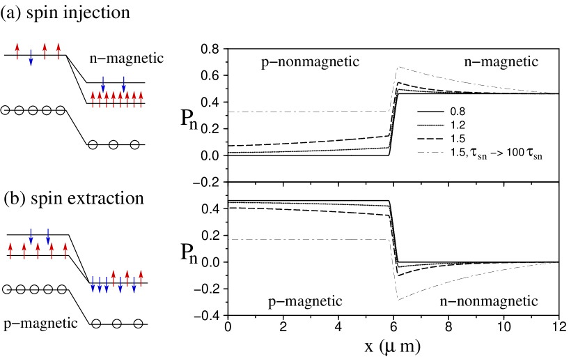
We first ask whether spin can be injected and extracted into/from the nonmagnetic region. At small bias ( V) there is no spin injection or extraction. As the bias increases, the injection and extraction become large and are further enhanced with . The reason why there is no spin injection or extraction at small bias is that although there are exponentially more spin up than spin down electrons (recall the Boltzmann statistics) in the magnetic side, the barrier for crossing the space-charge region is exponentially larger for spin up than for spin down electrons (see Fig. 4). Those two exponential effects cancel out, leaving no net spin current flowing through the space-charge region. We could examine these arguments with analytical findings from Eq. (24) also valid for low-bias regime. Considering spin injection in the nonmagnetic n-region () we see that in the absence of nonequilibrium spin polarization at , , there is indeed no spin injection: . This is in contrast to arguments which suggest that an inefficient spin injection arises from resistance (conductivity) mismatch Schmidt and Molenkamp (2002). Here we note that even with a good conductivity match and highly-polarized spin injector the spin injection can still be completely negligible. Furthermore, the efficiency of spin injection depends strongly on the applied bias rather than on the relative conductivities of the two regions.
At large bias self-consistent numerical results become indispensable, showing that spin injection/extraction is possible as a result of building up a nonequilibrium spin at the space-charge region. However, some of these trends, including our prediction for spin extraction, can already be seen analytically in the low bias regime, Using the previous assumption that are constant for and by solving diffusion equations for and we can obtain Fabian et al. (2002a)
| (30) |
where
| (31) |
implies that a contribution to the nonequilibrium spin in the n-region will have the opposite sign to that of the equilibrium spin in the p-region. Similar spin extraction was recently observed experimentally in MnAs/GaAs junctions Stephens et al. (2004) and related theoretical implications due to tunneling from nonmagnetic semiconductors into metallic ferromagnets were considered Bratkovsky and Osipov (2004). Furthermore, it was suggested that a combination of spin injection and spin extraction could lead to completely spin polarized carriers in semiconductor nanostructrures Osipov et al. (2005); Petukhov et al. (2006).
We next consider a simple scheme of a magnetic p-n junction, depicted in Fig. 5, in which there is an external source of nonequilibrium spin, induced optically or electrically. As we discuss below, an interplay between the equilibrium spin polarization and the nonequilibrium spin source leads to the spin-voltaic effect (a spin analog of the photo-voltaic effect) and to giant magnetoresistance.

Similar to the theory of charge transport in nonmagnetic junctions Shockley (1950) the total charge current can be expressed as the sum of minority carrier currents at the depletion edges with
| (32) |
where is given by Eq. (25) with , , and is the applied bias (positive for forward bias). Eq. (29) implies that in the regime of large spin splitting, , the density of minority electrons changes exponentially with () and can give rise to exponentially large magnetoresistance Žutić et al. (2002).
The interplay between the [recall Eq. (15)] in the p-region, and the nonequilibrium spin source of polarization in the n-region, at the edge of the depletion region, modifies the characteristics of the diodes. To illustrate the characteristics of magnetic p-n junction, consider the small-bias limit [recall Eqs. (16)-(28)] in the configuration of Fig. 5. The electron contribution to the total electric current can be expressed from Eqs. (25) and (32) as Žutić et al. (2002); Fabian et al. (2002a)
| (33) |
Equation (33) generalizes the Silsbee-Johnson spin-charge coupling Silsbee (1980); Johnson and Silsbee (1985), originally proposed for ferromagnet/paramagnet metal interfaces, to the case of magnetic p-n junctions. The advantage of the spin-charge coupling in p-n junctions, as opposed to metals or degenerate systems, is the nonlinear voltage dependence of the nonequilibrium carrier and spin densities Žutić et al. (2002); Fabian et al. (2002a), allowing for the exponential enhancement of the effect with increasing . Equation (33) can be understood qualitatively from Fig. 5. In equilibrium, and , no current flows through the depletion region, as the electron currents from both sides of the junction balance out. The balance is disturbed either by applying bias or by selectively populating different spin states, making the flow of one spin species greater than that of the other. In the latter case, the effective barriers for crossing of electrons from the to the side is different for spin up and down electrons (see Fig. 5). Current can flow even at when . This is an example of the spin-voltaic effect, in which nonequilibrium spin causes an EMF Žutić et al. (2002); Žutić and Fabian (2003) and the direction of the zero-bias current is controlled by the relative sign of and . We emphasize here that the spin-voltaic effect results in a build up of electrical voltage due to the proximity of the equilibrium and nonequilibrium spin. This effect is distinct from the so-called spin Hall effect(s) which results in a build up of a spin imbalance (different chemical potential for spin up and down), but no electric field, due to transport in a spin-orbit field Tse et al. (2005).
A straightforward method for detecting the spin-voltaic effect follows from the symmetry properties of the different contributions to the charge current under magnetization reversal. By reversing the equilibrium spin polarization using a modest external magnetic field () a part of , odd under such reversal, can be identified as the spin-voltaic current Žutić et al. (2002). Measurements of would then provide: (1) cancellation of contributions to the charge current that are not related to the injected spin; (2) a choice of to facilitate a sufficiently large for accurate detection. Unlike the spin LEDs, this approach does not rely on direct band-gap material and injected spin could be detected even in silicon Žutić et al. (2006a). Magnetic semiconductors approximately lattice matched with Si could be used for spin injection and detection [(Ga,Mn)As was already grown on Si Zhao et al. (2002)]. For example, the Mn-doped chalcopyrite ZnGeP2 (mismatch ) Ishida et al. (2003) has been reported to be ferromagnetic at room temperature. Another Mn-doped chalcopyrite, ZnSiP2, was recently predicted Erwin and Žutić (2004) to be ferromagnetic, as well as highly spin polarized and closely lattice-matched with Si (mismatch ). Mn doping of the chalcopyrite alloy ZnGe1-xSixP2 would likely lead to an exact lattice match, since the lattice constant of Si is between those of closely matched ZnSiP2 and ZnGeP2.
Additionally, from one could also determine a spin relaxation time by all-electrical means Žutić et al. (2003). A particular assumption of a magnetic homojunction is not essential. One could also generalize this analysis to heterojunctions which would include (see Fig. 3) band offsets and spin splitting in both conduction and valence bands.
Several experimental efforts have recently observed the spin-voltaic effect in semiconductor heterojunctions. One of the approaches used p-n (In,Ga)As/(Al,Ga)As heterojunction Kondo et al. (2006) in the applied magnetic field. Circularly polarized light was used to inject nonequilibrium spin in (Al,Ga)As while an applied magnetic field created equilibrium spin splitting in (In,Ga)As [a particular Al-composition in (Al,Ga)As-region can produce nearly zero -factor]. An interesting implication of this device is that it operates as a spin-photodiode Kondo et al. (2006). By converting circular polarization directly into an electrical signal it is a counterpart of a spin LED which converts electrical signal into emission of circularly polarized light. In another approach both the spin injection and the detection were realized electrically. Iron was used as a spin injector into n-doped GaAs, while the spin splitting in p-doped (Ga,Mn)As enabled spin detection Chen et al. (2006).
We will revisit the implications of spin-voltaic effect in three-terminal structures, discussed in the section on magnetic bipolar transistors.
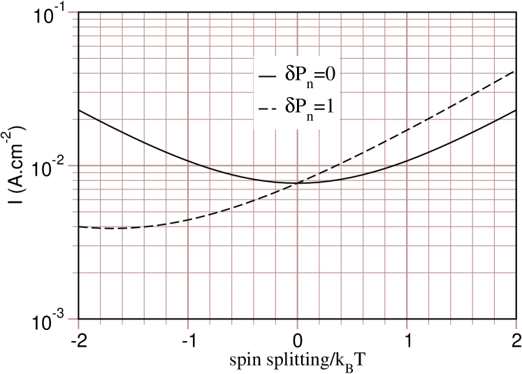
In addition to the spin-voltaic effect, the spin-charge coupling in magnetic p-n junctions can produce a giant magnetoresistance (GMR)-like effect, which follows from Eq. (33) Žutić et al. (2002). The current depends strongly on the relative orientation of the nonequilibrium spin and the equilibrium magnetization. Figure 6 plots , which also includes the contribution from holes, as a function of for both the unpolarized, , and fully polarized, , n-region. In the first case is a symmetric function of , increasing exponentially with increasing due to the increase in the equilibrium minority carrier density . In unipolar systems, where transport is due to the majority carriers, such a modulation of the current is not likely, as the majority carrier density is fixed by the density of dopants. A realization of exponential magnetoresistance was recently demonstrated in a very different materials system of manganite-titanate heterojunctions Nakagawa et al. (2005) in which an applied magnetic field affected the width of a depletion layer.
If , the current will depend on the sign of . For parallel nonequilibrium (in the n-region) and equilibrium spins (in the p-region), most electrons cross the depletion region through the lower barrier (see Fig. 5), increasing the current. In the opposite case of antiparallel relative orientation, electrons experience a larger barrier and the current is inhibited. This is demonstrated in Fig. 6 by the strong asymmetry in . The corresponding GMR ratio, the difference between for parallel and antiparallel orientations, can also be calculated analytically from Eq. (33) as Fabian et al. (2002a).
.3 3. Spin Transistors
Thus far we have mostly considered two-terminal spintronic devices in which we were concerned with spin injection and spin-voltaic phenomena. However, the greatest strength of the semiconductor spintronics should lie in the possibility to fabricate three-terminal structures that would allow current gain. Two goals can be set: First, to extend the functionalities of the existing transistors by adding spin control, and, second, to improve the performance of the current technology in terms of speed, power consumption, or sensitivity. Whether or not these goals will be reached depends much on the progress in fabrication and materials development, as well as on our understanding of the physics of spin-charge coupling in semiconductor heterojunctions.
We will briefly discuss a few proposed and existing spin transistor designs (some of them are further reviewed in Ref. Žutić et al. (2004)), before we analyze in more detail our proposal for magnetic bipolar transistors. The canonical example of a spin transistor is that of Datta and Das Datta and Das (1990), depicted in Fig. 1. The gating does not involve charge build up so the transistor could be faster and less power consuming than conventional field effect transistors. In addition, the magnetic configurations of the electrodes can be useful for storing information. However, despite many experimental efforts, the Datta-Das transistor has not been realized. There are inherent difficulties in its semiconductor-based design, the most important being the spin injection to the quasi one dimensional conduction channel (which, as noted in Sec. 1, could be avoided by using carbon nanotubes). An interesting alternative to the spin field-effect transistor, a spin MOSFET, has been a more conventional structure employing ferromagnetic source and drain and using the spin-valve effect to control the current Sugahara and Tanaka (2004, 2005). Since the proposed structure includes silicon substrate it could be potentially useful for silicon spintronics. An important prerequisite for spin MOSFET would be a demonstration of efficient spin injection in Si Žutić et al. (2006a) and there are recent efforts to fabricate suitable ferromagnet/Si contacts Min et al. (2006); Žutić (2006). Another effort to incorporate silicon in spintronics devices relies on spin diffusion transistor with silicon base Dennis et al. (2003). The emitter and collector contacts are ferromagnetic metal-insulator-semiconductor junctions and early encouraging results show both magnetoresistive effects and current gain greater than unity.
There have been other transistor designs using metallic layers in the structure. They go under the name of hot electron spin transistors or spin-valve transistors Žutić et al. (2004); Jansen (2003). For example, one realization (which is also called the magnetic tunneling transistor) uses a combination of a ferromagnetic tunnel junction and a Schottky barrier collector Mizushima et al. (1997); Yamauchi and Mizushima (1998); Sato and Mizushima (2001); van Dijken et al. (2002); van Dijken et al. (2003a, b). The tunnel junction plays the role of the emitter-base junction, supplying hot spin-polarized electrons into the magnetic base. The base-collector junction is a Schottky barrier. The hot electrons from the base can overcome the barrier only if their energy is higher than the barrier height. Since the hot electrons lose their energy depending on the spin, the magnetic junction can effectively control the collector current: for parallel magnetizations of the junction the current is large, while for antiparallel it is small, since the spin up, say, hot electrons in a spin down base equilibrate more efficiently than in a spin up base. This is the physics behind the high magnetocurrent rations (reaching thousands of percents) in these transistors. The disadvantage of these hybrid metal/semiconductor transistors is the absence of gain (the word transistor here points to the three-terminal geometry rather than to the ability to amplify currents). Nevertheless the hybrid designs have been successful in achieving the large magnetocurrent ratios and spin injection into semiconductors. A direct connection of such structures with bipolar transport, discussed in this manuscript, was recently realized in the spin-valve structures which contain a nonmagnetic p-n junction which can have useful effects as the energy barrier Huang et al. (2004, 2005).
Motivated by the potential ease of the integration of magnetic semiconductors with conventional devices we have proposed what we call magnetic bipolar transistors (MBT), in which one or more regions (emitter, base, and collector) are formed by a magnetic or ferromagnetic semiconductor Fabian et al. (2002b). We have shown that such structures can exhibit giant magnetoamplification, a significant control of electrical properties by magnetic field, as well as spin injection all the way from the emitter to the collector. The magnetic bipolar transistor was later discussed in terms of spin currents in Ref. Flatté et al., 2003 and in terms of magnetoamplification in Ref. Lebedeva and Kuivalainen, 2003. A bipolar transistor-like scheme has been recently presented in Ref. Dery et al. (2006): the semiconductor spin-diffusive channel is topped with three ferromagnetic electrodes, enabling the amplification of magnetoresistance.
.4 4. Magnetic Bipolar Transistors

.4.1 4.1 Connection to Bipolar Junctions Transistors
We next describe the operation principles of the magnetic bipolar transistor and their conventional (nonmagnetic) counterparts. Consider an npn transistor, as in Fig. 7a. The transistor consists of three regions: emitter, base, and collector. There are two p-n junctions in series: base-emitter and base-collector. Depending on the polarity of the bias across the junctions the transistor exhibits different functionalities. The current gain in bipolar junction transistors appear only in the active forward and active reverse regimes. In both regimes one junction is forward, the other reversed biased. The only distinction between the two regime comes from the asymmetry of the actual device. In the active forward bias the base-emitter junction is forward biased, while the base-collector junction is reverse biased. In the active reverse regime the bias polarities as switched. Typically the emitter is more heavily doped than the collector, which results in a much greater current gain for the active forward regime due to the increased electron injection efficiency from the emitter (see below).
There are two more possibilities for the transistor operation. In the saturation mode both of the junctions are forward biased. The transistor exhibits no gain, but this configuration is used in logic operations to represent the ON state. Similarly, the configuration in which both junctions are reverse biased, also called cutoff, is used to represent the OFF state.
We will see that those configurations have a much richer structure in magnetic bipolar transistors, shown schematically in Fig. 7b. In fact, there exists an additional configuration, in which both junctions are unbiased but spin-charge coupled (through the spin-voltaic effect), which can be used as a spin switch. All the possible functionalities are summarized in Table 1.
| mode | BJT | MBT | ||
|---|---|---|---|---|
| forward active | F | R | amplification | MA, GMA |
| reverse active | R | F | amplification | MA, GMA |
| saturation | F | F | ON | ON, GMA, SPSW |
| cutoff | R | R | OFF | OFF |
| spin-voltaic | 0 | 0 | OFF | SPSW |
We have seen in the Sec. 2.2 on magnetic diodes that the spin-charge coupling (or more specifically, the spin-voltaic effect) across magnetic p-n junctions can either intensify or inhibit carrier injection. The electron current in a magnetic junction was given by Eq. (33). This spin-charge coupling induces significant changes in the operation of the magnetic bipolar transistor in terms of what we have named magnetoamplification and giant magnetoamplification (GMA) Fabian et al. (2002b, 2004); Fabian and Žutić (2004, 2004).
Let us first see what is the mechanism behind the current gain in conventional bipolar transistors. The amplification factor is customarily written as Tiwari (1992)
| (34) |
Here
| (35) | |||||
| (36) |
and and are the base transport factor and the emitter injection efficiency, respectively. We can then call and the base transport inefficiency, which is due to the electron-hole recombination in the base, and emitter injection inefficiency, respectively.
The base transport inefficiency is given by the expression
| (37) |
which is valid for both conventional and magnetic transistors. Here is the width of the base and is the electron diffusion length. Typically the width of the base, , is much smaller than the electron diffusion length in the base, , in which case . Typically is about a micron, so the base transport factor does not play a significant role in modern bipolar transistors with a narrow base. Another possibility how to reduce the base factor is to employ graded semiconductors with built-in electric fields that help the diffusing electrons from the emitter to reach the collector faster to inhibit electron-hole recombination.
Unlike the base inefficiency, the emitter inefficiency depends rather strongly on the spin properties of the magnetic transistor. Let us write
| (38) |
where is the emitter inefficiency for conventional spin-unpolarized transistors, while the spin-charge coupling is contained in the factor . We can then write, for the practical limit of , that
| (39) |
We will be concerned only with ; is the conventional transistor current gain. For us it is just a numerical factor of the order of a hundred.
.4.2 4.2 Magnetoamplification
In the absence of an external spin injection, all the spin properties of magnetic bipolar transistors are determined by the equilibrium magnetization of the transistor regions. Similarly to magnetic diodes, this equilibrium magnetization influences electrical properties as well, due to the influence on the equilibrium minority carrier density. Consider a magnetic base, for example, assuming its spin polarization to be . The equilibrium electron density there is
| (40) |
where is the intrinsic density of the underlying semiconductor material and is the acceptor doping. Since the current across p-n junctions, in our case the emitter-base junction, is linearly dependent on , the electron emitter current and the emitter efficiency will be linearly proportional to as well. The spin-charge factor then stands out as
| (41) |
This finally gives for the gain of the transistor
| (42) |
It turns out that the gain can be controlled also by the emitter spin polarization Lebedeva and Kuivalainen (2003), but is unaffected by the possible equilibrium collector spin Fabian and Žutić (2004). The control of the current gain by the equilibrium spin polarization has been termed magnetoamplification Fabian et al. (2002a).
.4.3 4.3 Giant magnetoamplification
Giant magnetoamplification is a direct consequence of the spin-charge coupling across a p-n junction. Consider a magnetic bipolar transistor with a magnetic base having equilibrium spin polarization . The emitter and the collector are nonmagnetic. Suppose we can excite nonequilibrium spin in the emitter, giving it a nonequilibrium spin polarization . As a result of the proximity of the equilibrium and nonequilibrium spin there appears an EMF across the junction and the modification of the electron injection efficiency. This spin-charge coupling is reflected in the :
| (43) |
The current gain factor becomes
| (44) |
The spin dependence of the current gain due to the spin-charge coupling has been termed giant magnetoamplification Fabian and Žutić (2004), due to the potentially giant relative difference of amplification for parallel () and antiparallel () configurations. The corresponding giant magnetoamplification coefficient is
| (45) |
where the subscripts and represent the parallel and antiparallel configurations, respectively. For the above case of the magnetic base we obtain [recall also Sec. 2.2 and Eq. (33)]
| (46) |
If the equilibrium and nonequilibrium spin polarizations were about 50%, the corresponding GMA factor would be about 67%.
.4.4 4.4 Spin injection
We have seen in the previous section that spin injection from a magnetic n-region to a nonmagnetic p-region of a p-n junction is not possible at small biases due to balancing thermodynamics of the equilibrium spin polarization and the spin-dependent thermal activation. Only nonequilibrium spin can be injected, that is, the (nonequilibrium) spin has to first accumulate in the magnetic region.
Although the magnetic bipolar transistor comprises two magnetic p-n junctions in series, spin injection is possible even at low biases in the forward active regime. The reason for the possibility of spin injection is that minority electrons injected from the emitter to the magnetic base accumulate in the base. There is thus nonequilibrium electron density with a gradient sufficient to drive the electrons by diffusion to the collector. The electron spins equilibrate in the base to the equilibrium spin polarization. We thus have nonequilibrium spin density in the base, with the equilibrium spin polarization. It is this nonequilibrium spin density that drives the spin injection to the collector: as the spin-polarized electrons move towards the base-collector depletion layer, they are swept by the built-in electric field of the layer to the collector. In effect, we have a minority electron spin pumping, similar to what happens in spin-polarized p-n junctions or solar cells Žutić et al. (2001a). The resulting spin polarization in the collector, in the limit of a narrow base (the width smaller than the spin diffusion length), is Fabian and Žutić (2004)
| (47) |
where is the spin diffusion length in the collector and is the collector donor density. For a spin polarization of one can achieve as large as 0.1, mainly due to the large ratio of the base width and the spin diffusion length in the collector.
Much less surprising is the spin injection possibility for a source spin from the emitter to the collector. Suppose we induce a spin polarization in the emitter. In the active forward regime the spin is injected to the collector through the following sequence of steps: First, the source spin diffuses towards the base-emitter junction. If the spin diffusion length is larger than the length the spin travels from the injection point to the base-emitter depletion layer, the spin will attenuate only a little. Then the spin is transferred to the base through the depletion region. If we for now take a nonmagnetic base, the spin polarization in the base will be roughly . The nonequilibrium spin polarizations at the two sides of a p-n junction are the same, as follows from the generalized Shockley theory of spin-polarized p-n junctions Fabian et al. (2002a). As a result of the nonequilibrium spin polarization, there appears nonequilibrium spin density in the base. This density will be injected to the collector as a result of the minority electron spin pumping, similarly to the case of the no source spin case above. We have derived the following formula for the injected spin polarization in the collector:
| (48) |
Comparing with Eq. (47), we see that the role of the source spin polarization in the emitter is similar to the role of the equilibrium spin in the base. Both can be efficiently injected through to the collector.
In summary, magnetic bipolar transistors offer new functionalities to conventional semiconductor electronics. The most exciting is the possibility of large magnetoamplification effects. In all other aspects the magnetic bipolar transistors will have a similar performance to their conventional counterparts, since they are based on the same physical principles governing electronic transport.
.5 5. Conclusions
We have reviewed here several phenomena associated with bipolar spin-polarized transport in semiconductors. Our findings for two-terminal structures, such as magnetic heterojunctions, can also be applied to more complicated multi-terminal geometries. We show that the interplay of magnetic region with equilibrium spin polarization and injected nonequilibrium spin leads to the spin-voltaic effect in a heterojunction. This theoretical prediction, a spin-analog of the photo-voltaic effect, was also recently confirmed experimentally. The direction of the charge current, which can flow even at no applied bias, can be switched by reversal of the equilibrium magnetization or by reversal of the polarization of the injected spin. In three-terminal magnetic bipolar transistors the spin-voltaic effect implies that one could effectively control the gain or current amplification in such devices. We predict the possibility for giant magnetoamplification which could be viewed as a generalization of the spin-valve effect to semiconductor structures with strong intrinsic nonlinearities suitable for spin-controlled logic.
.6 Acknowledgements
We thank S. Das Sarma, M. Fuhrer, B. T. Jonker, H. Munekata, S. S. P. Parkin, A. Petrou, A. Petukhov, and E. I. Rashba for useful discussions. This work was supported by the US ONR, NSF-ECCS CAREER, DARPA, NRC-NRL, and SFB 689. This work was performed in part at SUNY’s Buffalo Center for Computational Research and used the resources of the Center for Computational Sciences and the Center for Nanophase Materials Sciences at Oak Ridge National Laboratory, which is supported by the Office of Science of the U.S. Department of Energy under Contract No. DE-AC05-00OR22725.
References
- Maekawa (2006) (Ed.) S. Maekawa (Ed.), Concepts in Spin Electronics (Oxford University Press, 2006).
- Maekawa and T. Shinjo (2002) (Eds.) S. Maekawa and T. Shinjo (Eds.), Spin Dependent Transport in Magnetic Nanostructures (Taylor and Francis, New York, 2002).
- Parkin et al. (2003) S. S. P. Parkin, X. Jiang, C. Kaiser, A. Panchula, K. Roche, and M. Samant, Proc. IEEE 91, 661 (2003).
- Prinz (1998) G. Prinz, Science 282, 1660 (1998).
- Ansermet (1998) J.-P. Ansermet, J. Phys.: Condens. Matter 10, 6027 (1998).
- Hartman (2000) (Ed.) U. Hartman (Ed.), Magnetic Multilayers and Giant Magnetoresistance (Springer, Berlin, 2000).
- Hirota et al. (2002) E. Hirota, H. Sakakima, and K. Inomata, Giant Magneto-Resistance Devices (Springer, Berlin, 2002).
- Gregg et al. (1997) J. Gregg, W. Allen, N. Viart, R. Kirschman, C. Sirisathitkul, J.-P. Schille, M. Gester, S. Thompson, P. Sparks, V. Da Costa, et al., J. Magn. Magn. Mater. 175, 1 (1997).
- Johnson (1994) M. Johnson, IEEE Spectrum 31, 47 (1994).
- Moodera and Mathon (1999) J. S. Moodera and G. Mathon, J. Mag. Magn. Mater. 200, 248 (1999).
- Parkin et al. (1999) S. S. P. Parkin, K. P. Roche, M. G. Samant, P. M. Rice, R. B. Beyers, R. E. Scheuerlein, E. J. O’Sullivan, S. L. Brown, J. Bucchigano, D. W. Abraham, et al., J. Appl. Phys. 85, 5828 (1999).
- Tehrani et al. (2000) S. Tehrani, B. Engel, J. M. Slaughter, E. Chen, M. DeHerrera, M. Durlam, P. Naji, R. Whig, J. Janesky, and J. Calder, IEEE Trans. Magn. 36, 2752 (2000).
- Johnson (2001) M. Johnson, J. Supercond. 14, 273 (2001).
- Žutić et al. (2004) I. Žutić, J. Fabian, and S. Das Sarma, Rev. Mod. Phys. 76, 323 (2004).
- Datta and Das (1990) S. Datta and B. Das, Appl. Phys. Lett. 56, 665 (1990).
- Bychkov and Rashba (1984) Y. A. Bychkov and E. I. Rashba, J. Phys. C 17, 6039 (1984).
- Winkler (2003) R. Winkler, Spin-Orbit Coupling Effecs in Two-Dimensional Electron and Hole Systems (Spinger, Berlin, 2003).
- Wang et al. (2003) B. Wang, J. Wang, and H. Guo, Phys. Rev. B 67, 092408 (2003).
- Schliemann et al. (2003) J. Schliemann, J. C. Egues, and D. Loss, Phys. Rev. Lett. 90, 146801 (2003).
- Matsuyama et al. (2002) T. Matsuyama, C.-M. Hu, D. Grundler, G. Meier, and U. Merkt, Phys. Rev. B 65, 155322 (2002).
- Mirales and Kirczenow (2001) F. Mirales and G. Kirczenow, Phys. Rev. B 64, 024426 (2001).
- Ciuti et al. (2002) C. Ciuti, J. P. McGuire, and L. J. Sham, Appl. Phys. Lett. 81, 4781 (2002).
- Nikonov and Bourianoff (2005) D. E. Nikonov and G. I. Bourianoff, IEEE Trans. Nanotech. 4, 206 (2005).
- Sugahara and Tanaka (2004) S. Sugahara and M. Tanaka, Appl. Phys. Lett. 84, 2307 (2004).
- Sugahara and Tanaka (2005) S. Sugahara and M. Tanaka, J. Appl. Phys. 97, 10D503 (2005).
- Schäpers et al. (2001) T. Schäpers, J. Nitta, h. B. Heersche, and T. Takayanagi, Phys. Rev. B 64, 125314 (2001).
- Sahoo et al. (2005) S. Sahoo, T. Kontos, J. F. annd C. Hoffman, M. Gräber, A. Cottet, and C. Schönenberger, Nature Phys. 1, 99 (2005).
- Žutić and Fuhrer (2005) I. Žutić and M. Fuhrer, Nature Phys. 1, 85 (2005).
- (29) This is a conventional meaning of the term bipolar, as used in the physics of semiconductors. However, the term bipolar has also been used to describe an analogy between the coexistence of two spin carrier populations (of spin up and spin down) in spin-polarized transport and two charge carrier populations (electrons and holes) in bipolar charge transport. See, for example, M. Johnson, Science 260, 320 (1993).
- Maekawa et al. (2002) S. Maekawa, S. Takahashi, and H. Imamura, in Spin Dependent Transport in Magnetic Nanostructures, edited by S. Maekawa and T. Shinjo (Taylor and Francis, New York, 2002), pp. 143–236.
- Shockley (1950) W. Shockley, Electrons and Holes in Semiconductors (D. Van Nostrand, Princeton, 1950).
- Sze (1981) S. M. Sze, Physics of Semiconductor Devices (John Wiley, New York, 1981).
- Fiederling et al. (1999) R. Fiederling, M. Kleim, G. Reuscher, W. Ossau, G. Schmidt, A. Waag, and L. W. Molenkamp, Nature 402, 787 (1999).
- Jonker et al. (2000) B. T. Jonker, Y. D. Park, B. R. Bennett, H. D. Cheong, G. Kioseoglou, and A. Petrou, Phys. Rev. B 62, 8180 (2000).
- Young et al. (2002) D. K. Young, E. Johnston-Halperin, D. D. Awschalom, Y. Ohno, and H. Ohno, Appl. Phys. Lett. 80, 1598 (2002).
- Hanbicki et al. (2003) A. Hanbicki, O. M. J. van t’Erve, R. Magno, G. Kioseoglou, C. H. Li, B. T. Jonker, G. Itskos, R. Mallory, M. Yasar, and A. Petrou, Appl. Phys. Lett. 82, 4092 (2003).
- Jiang et al. (2003) X. Jiang, R. Wang, S. van Dijken, R. Shelby, R. Macfarlane, G. S. Solomon, J. Harris, and S. S. P. Parkin, Phys. Rev. Lett. 90, 256603 (2003).
- Van Roy et al. (2006) W. Van Roy, P. Van Dorpe, J. De Boeck, and G. Borghs, Mater. Sci. Eng. B 126, 155 (2006).
- Janik and Karczewski (1988) E. Janik and G. Karczewski, Acta Physica Polonica A 73, 439 (1988).
- Munekata et al. (1989) H. Munekata, H. Ohno, S. von Molnár, A. Segmüller, L. L. Chang, and L. Esaki, Phys. Rev. Lett. 63, 1849 (1989).
- Ohno et al. (1992) H. Ohno, H. Munekata, T. Penney, S. von Molnár, and L. L. Chang, Phys. Rev. Lett. 68, 2664 (1992).
- Munekata et al. (1991) H. Munekata, H. Ohno, R. R. Ruf, R. J. Gambino, and L. L. Chang, J. Cryst. Growth 111, 1011 (1991).
- Ohno et al. (1996) H. Ohno, A. Shen, F. Matsukura, A. Oiwa, A. End, S. Katsumoto, and Y. Iye, Appl. Phys. Lett. 69, 363 (1996).
- Van Esch et al. (1997) A. Van Esch, L. Van Bockstal, J. De Boeck, G. Verbanck, A. S. van Steenbergen, P. J. Wellmann, B. Grietens, R. Bogaerts, F. Herlach, and G. Borghs, Phys. Rev. B 56, 13103 (1997).
- Hayashi et al. (1997) T. Hayashi, M. Tanaka, T. Nishinaga, H. Shimada, T. Tsuchiya, and Y. Otuka, J. Cryst. Growth 175/176, 1063 (1997).
- Ohno (1998) H. Ohno, Science 281, 951 (1998).
- Dietl (2002) T. Dietl, Semicond. Sci. Technol. 17, 377 (2002).
- Jungwirth et al. (2006) T. Jungwirth, J. Sinova, J. Masek, J. Kucera, and A. H. MacDonald (2006), eprint cond-mat/0603080.
- Ohno et al. (2000a) Y. Ohno, I. Arata, F. Matsukura, K. Ohtani, S. Wang, and H. Ohno, Appl. Surf. Sci. 159-160, 308 (2000a).
- Kohda et al. (2001) M. Kohda, Y. Ohno, K. Takamura, F. Matsukura, and H. Ohno, Jpn. J. Appl. Phys. 40, L1274 (2001).
- Johnston-Halperin et al. (2002) E. Johnston-Halperin, D. Lofgreen, R. K. Kawakami, D. K. Young, L. Coldren, A. C. Gossard, and D. D. Awschalom, Phys. Rev. B 65, 041306 (2002).
- Arata et al. (2001) I. Arata, Y. Ohno, F. Matsukura, and H. Ohno, Physica E 10, 288 (2001).
- Van Dorpe et al. (2004) P. Van Dorpe, Z. Liu, W. V. Roy, V. F. Motsnyi, M. Sawicki, G. Borghs, and J. De Boeck, Appl. Phys. Lett. 84, 3495 (2004).
- Tsui et al. (2003) F. Tsui, L. Ma, and L. He, Appl. Phys. Lett. 83, 954 (2003).
- Dietl (2003) T. Dietl, Nature Mater. 2, 646 (2003).
- Samarth et al. (2003) N. Samarth, S. H. Chun, K. C. Ku, S. J. Potashnik, and P. Schiffer, Solid State Commun. 127, 173 (2003).
- Park et al. (2002) Y. D. Park, A. T. Hanbicki, S. C. Erwin, C. S. Hellberg, J. M. Sullivan, J. E. Mattson, T. F. Ambrose, A. Wilson, G. Spanos, and B. T. Jonker, Science 295, 651 (2002).
- Li et al. (2005) A. P. Li, J. Shen, J. R. Thompson, and H. H. Weitering, Appl. Phys. Lett. 86, 152507 (2005).
- Koshihara et al. (1997) S. Koshihara, A. Oiwa, M. Hirasawa, S. Katsumoto, Y. Iye, S. Urano, H. Takagi, and H. Munekata, Phys. Rev. Lett. 78, 4617 (1997).
- Oiwa et al. (2002) A. Oiwa, Y. Mitsumori, R. Moriya, T. Supinski, and H. Munekata, Phys. Rev. Lett. 88, 137202 (2002).
- Ohno et al. (2000b) H. Ohno, D. Chiba, F. Matsukura, T. O. E. Abe, T. Dietl, Y. Ohno, and K. Ohtani, Nature 408, 944 (2000b).
- De Boeck et al. (1996) J. De Boeck, R. Oesterholt, A. Van Esch, H. B. r, C. Bruynseraede, C. Van Hoof, and G. Borghs, App. Phys. Lett. 68, 2744 (1996).
- Nazmul et al. (2005) A. M. Nazmul, T. Amemiya, Y. Shuto, S. Sugahara, and M. Tanaka, Phys. Rev. Lett. 95, 017201 (2005).
- Saito et al. (2003) H. Saito, V. Zayets, S. Yamagata, and K. Ando, Phys. Rev. Lett. 90, 207202 (2003).
- Pearton et al. (2003) S. J. Pearton, C. R. Abernathy, M. E. Overberg, G. T. Thaler, D. P. Norton, N. Theodoropoulou, A. F. Hebard, Y. D. Park, F. Ren, J. Kim, et al., J. Appl. Phys. 93, 1 (2003).
- Erwin and Žutić (2004) S. C. Erwin and I. Žutić, Nature Mater. 3, 410 (2004).
- Rashba (2000) E. I. Rashba, Phys. Rev. B 62, R16267 (2000).
- Smith and Silver (2001) D. L. Smith and R. N. Silver, Phys. Rev. B 64, 045323 (2001).
- Fert and Jaffres (2001) A. Fert and H. Jaffres, Phys. Rev. B 64, 184420 (2001).
- Zega et al. (2006) T. J. Zega, A. T. Hanbicki, S. C. Erwin, I. Žutić, G. Kioseoglou, C. H. Li, B. T. Jonker, and R. M. Stroud, Phys. Rev. Lett 96, 196101 (2006).
- Parkin et al. (2004) S. S. P. Parkin, C. Kaiser, A. Panchula, P. Rice, M. Samant, and S.-H. Yang, Nature Mater. 3, 862 (2004).
- Yuasa et al. (2004) S. Yuasa, T. Nagahama, A. Fukushira, Y. Suzuki, and K. Ando, Nature Mater. 3, 868 (2004).
- Butler et al. (2001) W. H. Butler, X. Zhang, T. C. Schulthes, and J. M. MacLaren, Phys. Rev. B 63, 054416 (2001).
- Mathon and Umerski (2001) J. Mathon and A. Umerski, Phys. Rev. B 63, 220403 (2001).
- Jiang et al. (2005) X. Jiang, R. Wang, R. M. Shelby, R. M. Macfarlane, S. R. Bank, J. S. Harris, and S. S. P. Parkin, Phys. Rev. Lett. 94, 056601 (2005).
- Wang et al. (2005) R. Wang, X. Jiang, R. M. Shelby, R. M. Macfarlane, S. S. P. Parkin, S. R. Bank, and J. S. Harris, Appl. Phys. Lett. 86, 052901 (2005).
- Salis et al. (2005) G. Salis, R. Wang, X. Jiang, R. M. Shelby, S. S. P. Parkin, S. R. Bank, and J. S. Harris, Appl. Phys. Lett. 87, 262503 (2005).
- Mott (1936) N. F. Mott, Proc. R. Soc. London, Ser. A 153, 699 (1936).
- Jonker et al. (2004) B. T. Jonker, A. T. Hanbicki, D. T. Pierece, and M. D. Stiles, J. Magn. Magn. Mater. 277, 24 (2004).
- Gijs and Bauer (1997) M. A. M. Gijs and G. E. W. Bauer, Adv. Phys. 46, 285 (1997).
- Johnson and Silsbee (1988) M. Johnson and R. H. Silsbee, Phys. Rev. B 37, 5312 (1988).
- Stiles and Zangwill (2002) M. D. Stiles and A. Zangwill, Phys. Rev. B 66, 014407 (2002).
- Hershfield and Zhao (1997) S. Hershfield and H. L. Zhao, Phys. Rev. B 56, 3296 (1997).
- Rashba (2002) E. I. Rashba, Eur. Phys. J. B 29, 513 (2002).
- Takahashi and Maekawa (2003) S. Takahashi and S. Maekawa, Phys. Rev. B 67, 052409 (2003).
- Jonker et al. (2003) B. T. Jonker, S. C. Erwin, A. Petrou, and A. G. Petukhov, MRS Bull. 28, 740 (2003).
- Jedema et al. (2001) F. J. Jedema, A. T. Filip, and B. J. van Wees, Nature 410, 345 (2001).
- Valet and Fert (1993) T. Valet and A. Fert, Phys. Rev. B 48, 7099 (1993).
- Johnson and Silsbee (1985) M. Johnson and R. H. Silsbee, Phys. Rev. Lett. 55, 1790 (1985).
- Garzon et al. (2005) S. Garzon, I. Žutić, and R. A. Webb, Phys. Rev. Lett 94, 176601 (2005).
- Godfrey and Johnson (2006) R. Godfrey and M. Johnson, Phys. Rev. Lett. 95, 136601 (2006).
- Žutić et al. (2001a) I. Žutić, J. Fabian, and S. Das Sarma, Phys. Rev. B 64, 121201 (2001a).
- Žutić et al. (2002) I. Žutić, J. Fabian, and S. Das Sarma, Phys. Rev. Lett. 88, 066603 (2002).
- Fabian et al. (2002a) J. Fabian, I. Žutić, and S. Das Sarma, Phys. Rev. B 66, 165301 (2002a).
- Meier and Zakharchenya (1984) (Eds.) F. Meier and B. P. Zakharchenya (Eds.), Optical Orientation (North-Holand, New York, 1984).
- Žutić et al. (2006a) I. Žutić, J. Fabian, and S. C. Erwin, Phys. Rev. Lett. 97, 026602 (2006a).
- Žutić et al. (2001b) I. Žutić, J. Fabian, and S. Das Sarma, Appl. Phys. Lett. 79, 1558 (2001b).
- Žutić et al. (2003) I. Žutić, J. Fabian, and S. Das Sarma, Appl. Phys. Lett. 82, 221 (2003).
- Ashcroft and Mermin (1976) N. W. Ashcroft and N. D. Mermin, Solid State Physics (Sounders, Philadelphia, 1976).
- Tse et al. (2005) W.-K. Tse, J. Fabian, I. Žutić, and S. Das Sarma, Phys. Rev. B 72, 214303 (2005).
- Weisbuch (1977) C. Weisbuch, Ph.D. Thesis (Paris Univ. VIII) p. 26 (1977).
- Dzhioev et al. (1997) R. I. Dzhioev, B. P. Zakharchenya, V. L. Korenev, and M. N. Stepanova, Fiz. Tverd. Tela 39, 1975 (1997), [Phys. Solid State 39, 1765-1768 (1997)].
- Kikkawa and Awschalom (1998) J. M. Kikkawa and D. D. Awschalom, Phys. Rev. Lett. 80, 4313 (1998).
- Dzhioev et al. (2001) R. I. Dzhioev, B. P. Zakharchenya, V. L. Korenev, D. Gammon, and D. S. Katzer, Zh. Eksp. Teor. Fiz. Pisma Red. 74, 182 (2001), [JETP Lett. 74, 200-203 (2001)].
- Hilton and Tang (2002) D. J. Hilton and C. L. Tang, Phys. Rev. Lett. 89, 146601 (2002).
- Žutić et al. (2006b) I. Žutić, J. Fabian, and S. C. Erwin, IBM J. Res. & Dev. 50, 121 (2006b).
- Ganichev and Prettl (2003) S. D. Ganichev and W. Prettl, J. Phys.: Condens. Matter. 15, R935 (2003).
- Long et al. (2003) W. Long, Q.-F. Sun, H. Guo, and J. Wang, Appl. Phys. Lett. 83, 1397 (2003).
- Mal’shukov et al. (2003) A. G. Mal’shukov, C. S. Tang, C. S. Chu, and K. A. Chao, Phys. Rev. B 68, 233307 (2003).
- Datta (2005) S. Datta, Appl. Phys. Lett. 87, 013115 (2005).
- Pershin and Privman (2003) Y. V. Pershin and V. Privman, Phys. Rev. Lett. 90, 256602 (2003).
- Furdyna (1988) J. K. Furdyna, J. Appl. Phys. 64, R29 (1988).
- Dietl (1994) T. Dietl, in Handbook of Semiconductors, Vol. 3, edited by T. S. Moss and S. Mahajan (North-Holland, New York, 1994), p. 1251.
- Zudov et al. (2002) M. A. Zudov, J. Kono, Y. H. Matsuda, T. Ikaida, N. Miura, H. Munekata, G. D. Sanders, Y. Sun, and C. J. Stanton, Phys. Rev. B 66, 161307 (2002).
- Deutsch et al. (2004) M. Deutsch, G. Vignale, and M. F. Flatté, J. Appl. Phys. 96, 7424 (2004).
- Schmeltzer et al. (2003) D. Schmeltzer, A. Saxena, A. Bishop, and D. L. Smith, Phys. Rev. B 68, 195317 (2003).
- Schmidt and Molenkamp (2002) G. Schmidt and L. W. Molenkamp, Semicond. Sci. Technol. 17, 310 (2002).
- Stephens et al. (2004) J. Stephens, J. Berezovsky, J. P. McGuire, L. J. Sham, A. C. Gossard, and D. D. Awschalom, Phys. Rev. Lett. 93, 097602 (2004).
- Bratkovsky and Osipov (2004) A. M. Bratkovsky and V. V. Osipov, J. Appl. Phys. 96, 4525 (2004).
- Osipov et al. (2005) V. V. Osipov, A. G. Petukhov, and V. N. Smelyankiy, Appl. Phys. Lett. 87, 202112 (2005).
- Petukhov et al. (2006) A. G. Petukhov, V. N. Smelyankiy, and V. V. Osipov (2006), eprint cond-mat/0609599.
- Silsbee (1980) R. H. Silsbee, Bull. Magn. Reson. 2, 284 (1980).
- Žutić and Fabian (2003) I. Žutić and J. Fabian, Mater. Trans., JIM 44, 2062 (2003).
- Zhao et al. (2002) J. H. Zhao, F. Matsukara, E. Abe, D. Chiba, Y. Ohno, K. Takamura, and H. Ohno, J. Cryst. Growth 237-239, 1349 (2002).
- Ishida et al. (2003) Y. Ishida, D. D. Sarma, K. Okazaki, J. O. J. I. Hwang, H. Ott, A. Fujimori, G. A. Medvedkin, T. Ishibashi, and K. Sato, Phys. Rev. Lett. 91, 107202 (2003).
- Kondo et al. (2006) T. Kondo, J. Hayafuji, and H. Munekata, Jpn. J. Appl. Phys. 45, L663 (2006).
- Chen et al. (2006) P. Chen, J. Moser, P. Kotissek, J. Sadowski, M. Zenger, D. Weiss, and W. Wegscheider (2006), eprint cond-mat/0608453.
- Nakagawa et al. (2005) N. Nakagawa, M. Asai, Y. Mukunoki, T. Susaki, and H. Y. Hwang, Appl. Phys. Lett. 86, 082504 (2005).
- Min et al. (2006) B.-C. Min, K. Motohashi, C. Lodder, and R. Jansen, Nature Mater. 5, 817 (2006).
- Žutić (2006) I. Žutić, Nature Mater. 5, 771 (2006).
- Dennis et al. (2003) C. L. Dennis, C. V. Tiusan, R. A. Ferreira, J. F. Gregg, G. J. Ensell, S. M. Thompson, and P. P. Freitas, J. Magn. Magn. Mater. 1383, 290 (2003).
- Jansen (2003) R. Jansen, J. Phys. D. Appl. Phys. 36, R289 (2003).
- Mizushima et al. (1997) K. Mizushima, T. Kinno, T. Yamauchi, and K. Tanaka, IEEE Trans. Magn. 33, 3500 (1997).
- Yamauchi and Mizushima (1998) T. Yamauchi and K. Mizushima, Phys. Rev. B 58, 1934 (1998).
- Sato and Mizushima (2001) R. Sato and K. Mizushima, Appl. Phys. Lett. 79, 1157 (2001).
- van Dijken et al. (2002) S. van Dijken, X. Jiang, and S. S. P. Parkin, Appl. Phys. Lett. 80, 3364 (2002).
- van Dijken et al. (2003a) S. van Dijken, X. Jiang, and S. S. P. Parkin, Appl. Phys. Lett. 82, 775 (2003a).
- van Dijken et al. (2003b) S. van Dijken, X. Jiang, and S. S. P. Parkin, Phys. Rev. Lett. 90, 197203 (2003b).
- Huang et al. (2004) Y. W. Huang, C. K. Lo, Y. D. Yao, L. C. Hsieh, J. J. Ju, D. R. Huang, and J. H. Huang, Appl. Phys. Lett. 85, 2959 (2004).
- Huang et al. (2005) Y. W. Huang, C. K. Lo, Y. D. Yao, L. C. Hsieh, and J. H. Huang, J. Appl. Phys. 97, 10D504 (2005).
- Fabian et al. (2002b) J. Fabian, I. Žutić, and S. Das Sarma (2002b), eprint cond-mat/0211639.
- Flatté et al. (2003) M. E. Flatté, Z. G. Yu, E. Johnston-Halperin, and D. D. Awschalom, Appl. Phys. Lett. 82, 4740 (2003).
- Lebedeva and Kuivalainen (2003) N. Lebedeva and P. Kuivalainen, J. Appl. Phys. 93, 9845 (2003).
- Dery et al. (2006) H. Dery, L. Cywinski, and L. J. Sham, Phys. Rev. B 73, 161307 (2006).
- Fabian and Žutić (2005) J. Fabian and I. Žutić, Appl. Phys. Lett. 86, 133506 (2005).
- Fabian et al. (2004) J. Fabian, I. Žutić, and S. D. Sarma, Appl. Phys. Lett. 84, 85 (2004).
- Fabian and Žutić (2004) J. Fabian and I. Žutić, Phys. Rev. B 69, 115314 (2004).
- Fabian and Žutić (2004) J. Fabian and I. Žutić, Acta Physica Polonica A 106, 109 (2004).
- Tiwari (1992) S. Tiwari, Compound Semiconductor Device Physics (Academic Press, San Diego, 1992).