Poisson Nernst-Planck Model of Ion Current Rectification
through a Nanofluidic Diode
Abstract
We have investigated ion current rectification properties of a recently prepared bipolar nanofluidic diode. This device is based on a single conically shaped nanopore in a polymer film whose pore walls contain a sharp boundary between positively and negatively charged regions. A semi-quantitative model that employs Poisson and Nernst-Plank equations predicts current-voltage curves as well as ionic concentrations and electric potential distributions in this system. We show that under certain conditions the rectification degree, defined as a ratio of currents recorded at the same voltage but opposite polarities, can reach values of over a at a voltage range . The role of thickness and position of the transition zone on the ion current rectification is discussed as well. We also show that rectification degree scales with the applied voltage.
pacs:
81.05.Zx, 02.60.Cb, 81.07.DeI Introduction
Nanopores in polymer films and silicon materials have attracted a lot of scientific interest due to their application as biomimetic systems for models of biological channels Lev et al. (1993); Siwy et al. (2003); Chen et al. (2004), and as biosensors Li et al. (2001); Dekker (2007); Harrell et al. (2006); Mara et al. (2004). Nanopores are also used as a basis for building ionic devices for controlling flow of ions and charged molecules in a solution Gijs (2007). In these systems electrostatic and hydrophobic interactions between the ions and molecules that pass through the pore and the pore walls are used to amplify or stop the transport. Our group has recently prepared a nanofluidic diode Vlassiouk and Siwy (2007) which rectifies ion current in a similar way as a bipolar semiconductor diode rectifies electron current. This diode is based on a single conically shaped nanopore in a polymer film with openings of and , respectively. The surface charge of the pore is patterned so that two regions of the pore with positive and negative surface charges create a sharp barrier called the transition zone. This nanofluidic diode is bipolar in character since both positively and negatively charged ions contribute to the measured current. Another type of nanofluidic diode was prepared in the group of A. Majumdar Karnik et al. (2007) with a sharp barrier between a positively charged zone and a neutral part of the pore. Presence of only one type of surface charges causes the latter device to be unipolar.
In this article we provide a semi-quantitative description of ion current rectification of the bipolar diode based on single conical nanopores. We use continuum mean-field theory, and more precisely Poisson and Nernst-Planck (PNP) equations, to define our model Schuss et al. (2001); Nadler et al. (2004); Chen et al. (1997); Liu et al. (2007) that we apply to describe current-voltage characteristics as well as profiles of ionic concentrations and electric potential in the system. Our model is based on a similar approach as described by Cervera et al. in Cervera et al. (2005, 2006). We would like to mention that the model of nanofluidic diode based on a rectangular channel with limiting length of tens of nanometers presented in Daiguji et al. (2005) combines PNP with Navier-Stokes equations. Nanopores considered here are significantly narrower with the smaller diameter around . Therefore, we consider here only PNP equations, because in nanopores of diameters less than , electrophoresis is known to be the most dominant process Daiguji et al. (2004); Karnik et al. (2007).
It is important to mention that continuum description of ion transport by the PNP equations has successfully rendered main properties of many biological channels, e.g. see Nonner and Eisenberg (1998) for the calcium channels treatment. When compared to more precise but computational expensive techniques, e.g. Brownian dynamics Corry et al. (2000), the continuum approach has a clear advantage in terms of computing cycles. As discussed in Corry et al. (2000) this description produces results which correctly render the physical and chemical phenomena occurring inside a cylindrical nanopore whose diameter is bigger than Debye lengths of the considered ionic species. Hence it is plausible to obtain valid results for the conical nanopores as long as their smallest diameter is bigger than Debye lengths in the examined system.
In this study, we thoroughly discuss how ion current rectification in a nanofluidic diode depends on the position of the transition zone between the two regions of pore walls with opposite surface charges. Influence of the width of the transition zone on rectifying properties of the device is studied in detail as well. We identify the range of values for the position of the transition zone and its width that lead to a significant enhancement of the current rectification degree. This aspect is of crucial importance for further improvement of these new devices. The paper is organized as follows. In section II we explain the experimental system and present the theoretical basis of our model. In section III we present the results of the analysis and provide directions to future improvements of the design of nanofluidic diodes.
II Methods
In this section we present the experimental results and the theoretical background which provide the basis of our simulations. In the first subsection we briefly explain the experimental facts which inspired the current project. The following subsections are devoted to the theoretical background.
II.1 Experimental
Single nanopores in polymer (polyethylene terephthalate, in short PET) film were prepared by the track-etching technique as described in Apel et al. (2001); Siwy (2006). Briefly, the method consists of irradiation of polymer films with single swift heavy ions Spohr (1983) (Gesellschaft fuer Schwerionenforschung, Darmstadt, Germany), and subsequent asymmetric etching of the irradiated foils at Apel et al. (2001). This procedure leads to preparation of membranes that contain only one pore with the small opening, called tip, as narrow as several nanometers in diameter, and the big opening, called base, with micrometer size diameter.
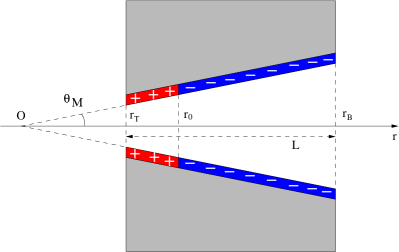
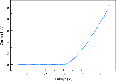
As the result of the chemical etching, there are carboxyl groups formed on the surface of pore walls with density of about one per , which determines the surface charge to Wolf-Reber (2002). In order to modify the surface of PET nanopores we used the method of coupling carboxyl and amine groups with 1-Ethyl-3-[3-dimethylaminopropyl]carbodiimide hydrochloride (EDC) Grabarek and Gergely (1990). The reaction between the carboxyl groups and diamines changes the surface charge from negative to positive. Targeted modification of the tip was obtained by introducing the reagent mixture only on the side of the membrane with the small opening Vlassiouk and Siwy (2007). The other side of the membrane was in contact with a buffer solution. A conical shape of the pore makes the distribution of the diamines and EDC in the pore extremely non-homogeneous. There is a high concentration of the reagents at the tip of the pore that assures the chemical modification reaction of the tip to occur. The concentration of diamines and EDC at the remaining part of the pore is very low, therefore this part remains negatively charged. As the result, we obtain a surface charge distribution as schematically shown in Fig. 1. An example of the current-voltage characteristic through such a device recorded at and is presented in Fig. 2. The rectification degree of the system is defined as the ratio of currents recorded for positive and negative voltages, respectively
| (1) |
The rectification degree of this system (Fig. 2) equals at Vlassiouk and Siwy (2007). We would like to mention that even devices with uniform surface charge distribution rectify the current but their rectification degree is one order of magnitude smaller than the one obtained for the systems described above Apel et al. (2001); Siwy et al. (2003).
II.2 Modeling
Before we start to introduce the theoretical base of the model we would like to specify the notation. We have assigned the subscripts “” and “” to designate the various physical quantities computed at the tip and at the base sides of the pore, respectively. In this sense is the location of the pore tip and is the location of the pore base. The thickness of the membrane is denoted with . The cone opening angle is . The membrane is immersed in an electrolyte containing potassium and chloride ions, and in addition we apply an external electric field with the help of two electrodes positioned far away from the membrane on each side of the pore. Due to resistance of single nanopores, the voltage drop will occur only inside the pore, not in the electrolyte bulk. By convention, we will keep the electrode on the pore tip side grounded such that the sign of the electric potential difference will be controlled by the electrode on the base side of the pore. The existence of the external field causes the ions to migrate towards the electrodes, which we record as ion current. We would like to mention that for small pores Siwy et al. (2003) and more complex electrolytes in which chemical reactions can occur, one observes large fluctuations of ion current in time Siwy et al. (2006a, b). However our model in its present form does not include chemical reactions between components of the electrolyte, and therefore the system will reach a stationary regime, i.e., the ionic fluxes are constant in time. In nanofluidic diodes, constant currents at constant voltages are indeed observed experimentally. Our goal is to compute the steady state current for a fixed set of physical and chemical parameters. Hence we express the stationarity of the ionic fluxes using Nernst-Plank condition. To be more specific we assume that for each ionic species, indexed by “”, the molar flux defined as
| (2) |
is conserved, i.e., it obeys the Nernst-Plank condition
| (3) |
where is the diffusion coefficient of an ion , is the molar concentration and is the charge number of the ion . We have denoted with the electric potential in units, which satisfies the Poisson equation
| (4) |
where is the electric permittivity of the medium and the summation is carried over all the ions present in the solution. The parameter is the Faraday constant, is the gas constant and is the absolute temperature. The PNP equations (3) and (4) provide a complete set of equations which together with appropriate boundary conditions allow us to determine the concentration of each ionic species and the electric potential inside the pore. Consequently the total ion current density along an arbitrary direction can be computed with the help of (2)
| (5) |
where the summation is performed again over all considered ions.
As the problem has azimuthal symmetry with respect to the pore axis, it gets reduced to a set of two-dimensional second order partial differential equations. To simplify the problem even more we perform an analytical integration with respect to the polar angle and we obtain a set of second order ordinary differential equations which is finally solved numerically. We would like to mention that after integration one has to neglect one term in order to obtain a well defined set of ordinary differential equations Cervera et al. (2006). Our comparison tests between the full two dimensional problem and the approximated one dimensional problem show insignificant differences in both the quantitative and the qualitative results. Hence the solution of the problem will provide averaged quantities in the sense that the polar angle dependence is lost during the integration. However our main interest is to compute the ion current, which involves averaging along the polar coordinate, therefore we do not loose any information. To be more specific, the differential equations which result from the above described procedure have the following structure
| (6) |
and
| (7) |
where the quantities and in (6) and (7) come from integration, i.e.,
| (8a) | ||||
| (8b) | ||||
and the function is given by
| (9) |
where represents the surface charge density. For simplicity we have kept the same notation for the averaged quantities and and we will use the functional dependence on the polar angle to distinguish between them and the non-averaged quantities and .
II.3 Boundary Conditions
To completely define the problem we have to specify the boundary conditions. These conditions are derived from the so called Donnan equilibrium conditions which express the thermodynamic equilibrium between the membrane with excess surface charge and the ionic concentrations in the bulk. One can derive these conditions as in Gillespie and Eisenberg (2001) and obtain the following relations for the concentrations at the pore border
| (10) |
where represents the bulk concentration of ion and indexes the tip and the base sides of the pore, respectively. is the Donnan potential defined as the potential difference created across an ion exchange membrane
| (11) |
where is the electric potential at the corresponding electrode. The electro-neutrality condition, which has the form
| (12) |
provides an equation for . Hence, the boundary conditions can be derived from (10) and (12) as
| (13) |
and
| (14) |
The PNP equations (6) and (7) together with the boundary conditions (13) and (14) form the base of our model. We deal with two ionic species in our system, i.e., and , therefore we have to solve a set of three second order ordinary differential equations.
II.4 Surface Charge Distribution
The charge distribution is formed by two distinct regions with positive and negative surface charges respectively, and a transition zone between them. These regions are characterized by the asymptotic values of the surface charge density, i.e., the value of far away from the transition zone. We employ some simplifying assumptions in order to characterize the surface charge distribution in the transition zone. Firstly, we consider that the magnitudes of the asymptotic values of the positive and negative surface charge densities are the same and equal to , where is the elementary charge. Additionally, we assume that the transition between the positive and negative charges on pore walls is made in a symmetric, continuous, and monotonic way.
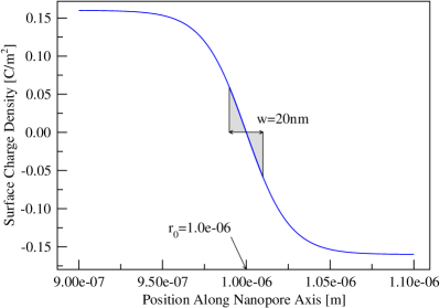
Hence we will consider the surface charge density in the pore to be described by the logistic type function (see Fig. 3):
| (15) |
where is the minimum value of the surface charge density, is the position along the pore axis where equals zero, and measures the slope of in the transition zone. Another equivalent way to characterize the charge distribution in the transition zone is to specify the transition zone width (see Fig. 3) which is defined as the part of the pore where the magnitude of the charge is bellow , i.e.,
| (16) |
where are constants. In this problem there are many parameters which can be modified. However our main interest was to see how the properties of the nanofluidic diode modify when the surface charge distribution parameters change. Therefore, we have chosen to keep all the parameters constant, the only exception being and , the parameters, which we believe can be controlled experimentally.
III Results
As we have discussed in the previous section we have to solve a boundary value problem (BVP) defined by a set of three second order ordinary differential equations. The solution will provide the potassium and chloride concentrations and the electric potential as functions of the coordinate along the pore axis. We have used the BVP solver described in Shampine et al. (2006) to compute the solution with an error less than . The solution of the computation is used to evaluate the ion current which is given by
| (17) |
where is the radial component of the ion current density given by (5). As we expect the current is not dependent on the radial coordinate and it has a constant value along the pore axis.
III.1 Current-voltage curves and ionic concentration profiles
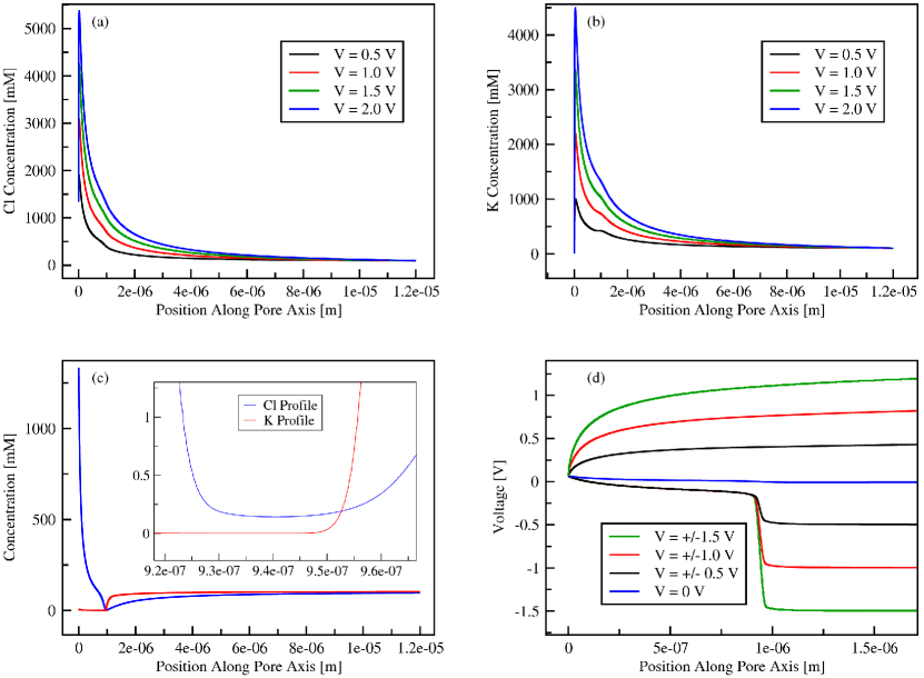
The system that we have considered is a single conical nanopore with pore diameters and , respectively, at symmetric electrolyte conditions of on both sides of the membrane. The thickness of the membrane is . Fig. 4(a-c) show the numerical solutions of the corresponding distributions of potassium and chloride ions in forward and reverse bias, respectively. Fig. 4(d) presents the distribution of the electric potential in the nanopore for various applied voltages. The increase of ionic concentrations in the forward bias is remarkable. Concentrations of both ions, potassium and chloride, have increased by an order of magnitude, compared to the bulk concentration of . This result also confirms bipolar character of our device, since and contribute almost equally to the measured ion current. Ionic concentrations at the reverse bias are dramatically different. We see significantly lower concentrations of both ions in a region close to the transition zone which indicates the formation of the depletion zone. The inset in Fig. 4(c) shows a magnified view of the depletion zone where the concentration of both ions drops practically to zero. This region is located slightly off the center of the transition zone because of the conical geometry of the nanopore. Fig. 4(d) shows profiles of electric potential in the pore for various voltages applied in the forward and reverse directions. Similar to the results for diodes based on rectangular channels and bipolar membranes Karnik et al. (2007); Daiguji et al. (2004); Bassignana and Reiss (1983); Mafé and Ramírez (1997), in our bipolar diode based on single conical nanopores, the whole voltage drop occurs in the depletion zone. This sudden drop of the electric potential causes the appearance of a huge electric field located in the depletion zone, which will effectively block the ionic currents in the reverse bias.
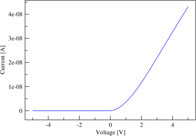
Using the numerical solution and Eq. (17) we compute the ion current. Fig. 5 shows a typical current-voltage curve calculated for this nanopore with parameters and . Similar to the experimental data shown in Fig. 2, the model predicts very high rectification degrees with very small ion currents for reverse bias.
III.2 Position of depletion zone, dynamics of nanofluidic diode formation
The process of preparation of nanofluidic diode is based on a chemical reaction of the reagent with the carboxyls groups on the pore walls. This causes change of the position and increase of the rectification degree in time when the chemical reaction progresses Vlassiouk and Siwy (2007).
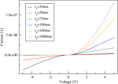
We decided to investigate in more details how sensitive the rectification degree is on the position of the transition zone in the pore. We performed therefore numerically the experiment of chemical modification of the pore walls. However, the reader must be aware that our surface charge distribution is not necessarily the distribution which corresponds to the real case. In the real case the shape of changes in time Vlassiouk and Siwy (2007), i.e., it changes with , whereas in our case, the time evolution is simply described by a translation of along the radial coordinate. We think however that the main features of the real charge distribution are present in our model system and this gives us the possibility to understand and get insight into the nanofluidic diode behavior when the surface charge gets modified. A given value of the transition zone width was assumed and the position was moved between the pore tip and its base. In other words, we start from the situation where the whole surface of the pore is negatively charged and finish in a state where the whole surface is positively charged. In the initial and final states we have a homogeneously charged conical geometry that leads to ion current rectification via rocking ratchet mechanism described earlier in Siwy and Fuliński (2002) and Siwy and Fuliński (2004). The rectification degree was defined in Eq. (1) as the ratio of currents recorded for positive voltages divided by currents recorded for negative voltages. These homogeneously charged conical nanopores are characterized by rectification degrees less than . As we move the position inside the pore the surface charge in the tip changes acquiring more positive charges. As shown in Fig. 6, it is remarkable that a small amount of positive charge in the tip of the pore reverses the direction of rectification and changes the devices from monopolar to bipolar. The rectification degree versus is shown in Fig. 7 for several values of the transition zone width.
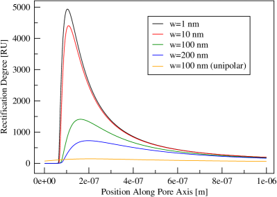
The rectification degree increases steeply as we move inside the pore along its axis, reaches a maximum, and decreases to a value lower than , when is located at the base of the pore. A very strong dependence of the rectification degree on , when is located at the narrowest part of the pore, suggests that transport properties of the system are determined by the physical and chemical properties of the tip of the nanopore, in this case the surface charge distribution. It is also important to mention that we have predicted higher currents for devices where is located further from the tip (e.g. at ). However, these devices show lower rectification degrees due to larger leakage currents (off state currents). Depending on the specifics of the various applications nanofluidic diodes can therefore provide higher (lower) currents and lower (higher) rectification degrees. We would like to emphasize that all these various properties can be obtained by just changing the position of the zero surface charge point.
As a comparison, we have also included rectification data for a monopolar diode designed such that the tip of the pore was positively charged () with the rest of the pore neutral (). The surface charge distribution is similar to the one shown in Fig. 3, the only difference is that represents in this case the position where the surface charge is half its maximum value. The parameter was set to . One can see that overall the rectification degrees for the monopolar diode are much smaller than in case of the bipolar diode when both devices are studied in the same concentration.
Our results show that a huge increase of ion current rectification degrees is possible when the surface of a pore is patterned such that a part of a pore with negative surface charge is brought into contact with a part of the pore with positive surface charge. Our analysis also points to the importance of future experimental efforts aimed at a better control over the width of the transition zone as well as the position of the center of a depletion zone.
III.3 Scaling of rectification degree with voltage
We have also analyzed the behavior of the rectification degree with voltage.
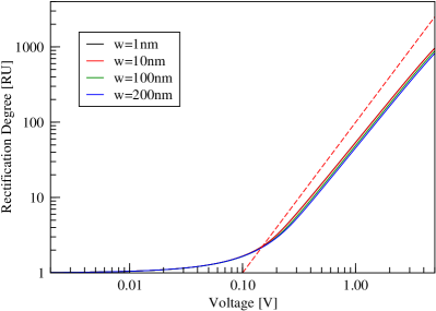
In Fig. 8 we show the rectification degree of a nanofluidic diode as a function of voltage ranging between and for the case when the transition zone is located away from the tip, and for various values of . We find that has a power law dependence for voltages larger than ,
| (18) |
where the scaling exponent . For guidance, the power law with exponent equal to is shown in Fig. 8. The power law scaling of the rectification degree with voltage might suggest the existence of universal scaling. To our knowledge, this is the first time when this scaling has been observed in the variation of the rectification degree with the applied voltage for a nanofluidic diode based on a single conical nanopore. The applicability of the universal scaling and universal scaling exponents to nanofluidic diodes will be investigated in our future studies.
III.4 Dependence of depletion zone width on voltage
Another interesting question to consider is the dependence of the depletion zone width on the reverse bias voltages. The depletion zone is defined as the region where mobile charges are absent or at least their number is small compared to adjacent regions Fig. 4. This ion free region appears only in the reverse bias regime. The lack of ions in this zone produces a drop of the electric potential, or in other words the electric field in this region is strong enough to block the migration of mobile charges through the pore. To help visualize the above statements we have superimposed in Fig. 9 the concentration profiles, the electric potential, and its first derivative which is proportional to the electric field. Since the voltage drops over a very small distance the electric fields created are of the order of magnitude .
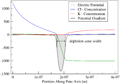
As we have explained above, the electric field has a strong peak in the depletion zone and we have considered the width of this peak to provide the definition for the width of the depletion zone. In order to plot all these profiles in one figure, scaling of their values was necessary. The electric potential was scaled up times and its first derivative was scaled down times such that all the graphs will provide sufficient details. The plots in Fig. 9 correspond to , , and for a reverse bias voltage of .
We would like to emphasize the difference between the width of the transition zone and the width of the depletion zone. Larger values lead to larger values of , as shown in Fig. 10.
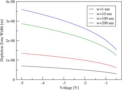
For equal to and , the resulting for exceeds the value of the transition zone width that assured formation of much smaller leakage currents, and consequently higher rectification degrees. For transition zone of width and , the depletion zone is narrower than the values of . Larger therefore does not necessarily imply higher rectification degrees, as explained in the previous section. Smaller values of and assure larger electric fields for the reverse bias, which also helps formation of a depletion zone of a larger resistance.
IV Conclusions
The modeling of a nanofluidic diode presented in this manuscript has been motivated and inspired by recent experimental realization of this device Vlassiouk and Siwy (2007). In this article we have shown that rectification degrees of can be achieved with this device upon more precise surface charge control. We have shown that the width of the transition zone and the position of the transition point are parameters which influence very strongly the rectification properties of nanofluidic diodes. These parameters in turn are controlled by chemical modification of pore walls. Our analysis also shows that preparation of a nanofluidic diode based on a conical geometry offers much freedom in tuning rectification properties of the device. Future experimental efforts will be focused on developing surface chemistries so that various rectification degrees can be obtained. Our modeling also provide directions for the future design of the nanofluidic diode in order to prepare versatile devices which meet the requirements of various applications.
It would be very interesting to see how the rectification behaves when other parameters of the problem are changed, for example shape of the nanopore, and magnitude of surface charge. Another interesting aspect of the bipolar diode is the power law dependence of rectification degrees on voltage, which might suggest existence of universal scaling and critical exponents in the system. Our future studies will be directed towards identification of these critical exponents and relating them to formation of the depletion zone.
Acknowledgements.
We are grateful to Dr. Ivan Vlassiouk for stimulating discussions, and Dr. Magdalena Constantin for careful reading of our manuscript. We thank the Alfred P. Sloan Foundation and the Institute for Complex Adaptive Matter for financial support.References
- Lev et al. (1993) A. A. Lev, Y. E. Korchev, T. K. Rostovtseva, C. L. Bashford, D. T. Edmonds, and C. A. Pasternak, Proceedings: Biological Sciences 252, 187 (1993).
- Siwy et al. (2003) Z. Siwy, P. Apel, D. Baur, D. D. Dobrev, Y. E. Korchev, R. Neumann, R. Spohr, C. Trautmann, and K.-O. Voss, Surf. Sci. 532-535, 1061 (2003).
- Chen et al. (2004) P. Chen, T. Mitsui, D. B. Farmer, J. Golovchenko, R. G. Gordon, and D. Branton, Nano Letters 4, 1333 (2004).
- Li et al. (2001) J. Li, D. Stein, C. McMullan, D. Branton, M. J. Aziz, and J. A. Golovchenko, Nature 412, 166 (2001).
- Dekker (2007) C. Dekker, Nature Nanotech. 2, 209 (2007).
- Harrell et al. (2006) C. C. Harrell, Y. Choi, L. P. Horne, L. A. Baker, Z. S. Siwy, and C. R. Martin, Langmuir 22, 10837 (2006).
- Mara et al. (2004) A. Mara, Z. Siwy, C. Trautmann, J. Wan, and F. Kamme, Nano Letters 4, 497 (2004).
- Gijs (2007) M. A. M. Gijs, Nature Nanotech. 2, 268 (2007).
- Vlassiouk and Siwy (2007) I. Vlassiouk and Z. S. Siwy, Nano Letters 7, 552 (2007).
- Karnik et al. (2007) R. Karnik, C. Duan, K. Castelino, H. Daiguji, and A. Majumdar, Nano Letters 7, 547 (2007).
- Schuss et al. (2001) Z. Schuss, B. Nadler, and R. S. Eisenberg, Phys. Rev. E 64, 036116 (2001).
- Nadler et al. (2004) B. Nadler, Z. Schuss, A. Singer, and R. S. Eisenberg, J. Phys.: Condens. Matter 16, S2153 (2004).
- Chen et al. (1997) D. Chen, J. Lear, and R. S. Eisenberg, Biophys. J. 72, 97 (1997).
- Liu et al. (2007) Q. Liu, Y. Wang, W. Guo, H. Ji, J. Xue, and Q. Ouyang, Phys. Rev. E 75, 051201 (2007).
- Cervera et al. (2005) J. Cervera, B. Schiedt, and P. Ramírez, Europhys. Lett. 71, 35 (2005).
- Cervera et al. (2006) J. Cervera, B. Schiedt, R. Neumann, S. Mafé, and P. Ramírez, J. Chem. Phys. 124, 104706 (2006).
- Daiguji et al. (2005) H. Daiguji, Y. Oka, and K. Shirono, Nano Letters 5, 2274 (2005).
- Daiguji et al. (2004) H. Daiguji, P. Yang, and A. Majumdar, Nano Letters 4, 137 (2004).
- Nonner and Eisenberg (1998) W. Nonner and B. Eisenberg, Biophys. J. 75, 1287 (1998).
- Corry et al. (2000) B. Corry, S. Kuyucak, and S. H. Chung, Biophys. J. 78, 2364 (2000).
- Apel et al. (2001) P. Y. Apel, Y. E. Korchev, Z. Siwy, R. Spohr, and M. Yoshida, Nucl. Instrum. and Met. in Phys. Res. B 184, 337 (2001).
- Siwy (2006) Z. Siwy, Adv. Funct. Mater. 16, 735 (2006).
- Spohr (1983) R. Spohr, “ Method for Producing Nuclear Traces or Microholes Originating from Nuclear Traces of an Individual Ion” (1983), “German Patent DE 2951376 C2; United States Patent 4369370”.
- Wolf-Reber (2002) A. Wolf-Reber, Ph.D. thesis (2002).
- Grabarek and Gergely (1990) Z. Grabarek and J. Gergely, Anal. Biochem. 185, 131 (1990).
- Coster (1965) H. G. L. Coster, Biophys. J. 5, 669 (1965).
- Bassignana and Reiss (1983) I. C. Bassignana and H. Reiss, J. Membr. Sci. 15, 27 (1983).
- Mafé and Ramírez (1997) S. Mafé and P. Ramírez, Acta Polym. 48, 234 (1997).
- Siwy et al. (2006a) Z. Siwy, M. R. Powell, E. Kalman, R. D. Astumian, and R. S. Eisenberg, Nano Letters 6, 473 (2006a).
- Siwy et al. (2006b) Z. Siwy, M. R. Powell, A. Petrov, E. Kalman, C. Trautmann, and R. S. Eisenberg, Nano Letters 6, 1729 (2006b).
- Gillespie and Eisenberg (2001) D. Gillespie and R. S. Eisenberg, Phys. Rev. E 63, 061902 (2001).
- Shampine et al. (2006) L. Shampine, P. Muir, and H. Xu, JNAIAM 1, 201 (2006).
- Siwy and Fuliński (2002) Z. Siwy and A. Fuliński, Phys. Rev. Lett. 89, 198103 (2002).
- Siwy and Fuliński (2004) Z. Siwy and A. Fuliński, Am. J. Phys. 72, 567 (2004).