Spatially resolved THz response as a characterization concept for nanowire FETs
Abstract
In this paper, we propose a THz probe technique to obtain spatially resolved information about the electronic spectra inside nanowire-based FETs. This spectroscopic approach employs a segmented multi-gate design for the local detection of quantum transitions between few-electron states within the FET channel. We simulate the intra-band THz response of such devices by means of a many-body quantum approach, taking quantization and Coulomb interaction effects into account. The obtained simulation results demonstrate the capabilities of the proposed technique which go beyond the limitations of standard characterization methods.
I Introduction
The electronic properties of ultimately scaled nanotransistors are dominated by only a handful of electrons or holes. In such nanodevices, one has to face two non-classical physical mechanisms. Firstly, due to the spatial confinement of charge carriers on a nanoscale, quantization energies of electronic states become relevant, leading to a non-classical transport behavior. Secondly, the details of the Coulomb interaction between the individual carriers become important and can no longer be described in terms of a classical mean-field picture. The consequences can be clearly observed experimentally for example in Coulomb blockade phenomena.
One-dimensional nanowire-based field effect transistors (FET) have recently attracted great interest due to their advantageous electrostatics and transport properties [1, 2, 3]. From a different perspective, they also represent prototypes for the study of technological as well as physical challenges in future transistor designs. Instead of considering quantization and Coulomb phenomena as unwanted deviations from the classical device behavior, here one actually utilizes such non-classical effects for the improvement of FET devices or for new functionalities in a future quantum information technology.
In order to understand and finally utilize the physics of quantization and Coulomb effects within such nanowire FETs, one needs a characterization technique that is able to probe quantum states. Typical quantum energy scales of few-electron states in realistic nanowire FETs are on the order of a few meV corresponding to the 100GHz-1THz frequency range. We therefore propose the concept of a spatially resolved THz probe to directly measure quantum transitions between few-electron (or -hole) states within a nanowire FET. This spectroscopic approach employs a multi-gate FET layout, thus being able to provide spatially resolved information about the electronic spectra and electronic charge distributions inside the FET channel. Such a concept goes beyond the capabilities of standard linear and nonlinear characterization methods [4]. In this paper, we discuss the theoretical aspects of the proposed multi-gate THz probe. We simulate the intra-band THz response of nanowire FET devices by means of a many-body quantum approach, taking quantization and Coulomb interaction effects beyond mean-field into account.
In the following sections, we first describe the main physical ideas behind our many-body THz simulation approach, and secondly, we demonstrate the strengths of the concept of a THz probe by discussing a realistic example of a multi-gate nanowire FET. As a main effect, we obtain the formation of a Wigner molecule in the long channel limit.
II Theoretical approach
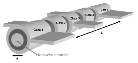
Fig. 1 shows a schematic sketch of the considered nanowire FET with multiple gate segments. We assume that only one lateral subband needs to be taken into account, corresponding to channel diameters in the sub-30 nm range for GaAs. In order to capture the numerous details of a real device structure, such as the actual geometrical configuration of the gate electrodes, a realistic quantum simulation of such a nanodevice requires the consideration of a sufficiently large number of single-particle states [5, 6]. In contrast to the commonly employed Anderson- or Hubbard-like many-body models [7, 8], in general we have to account for an inhomogeneous, anisotropic, and screened Coulomb interaction. Since the resulting many-body problem scales exponentially in , such a realistic simulation thus grows beyond any computational limit. In this context, we have recently introduced a multi-configurational approach (MCSCG, [3, 9, 10]) which employs a reduced adaptive basis for the simulation of Coulomb blockade phenomena in nanowire FETs. For the simulation of THz response, however, the number of considered basis states has yet to be increased. As a solution, we have therefore extended the MCSCG by a “bucket-brigade” algorithm (BBCI) [11, 12] which allows us to select a few thousand relevant many-body configurations from the exponentially growing basis set. A general few-electron state in turn can be written as a linear combination of such relevant configurations. This approach enables us to describe correlated many-body states beyond mean-field theory (e.g. Hartree-Fock or LDA-DFT [13]) which become essential within the field of quantum information technology. The following simulation results are based on the BBCI algorithm in combination with first-order Kubo theory [14] for the description of the THz response spectra within the chosen relavant many-body basis.
III Simulation results
For the following idealized example, the outer ends of the channel are covered by gate electrodes (for example gates 1 and 5 in Fig. 1). Applying a sufficiently large negative voltage to the outermost gates, barriers arise and we thus can assume an almost isolated channel system. The input THz excitation is applied to gate 1 (see Fig. 1), whereas the intermediate gate fingers (gates 2,3,4 in Fig. 1) serve as spatially resolved probes with zero DC bias. In our example, we consider two different GaAs-based nanowire MOSFETs with SiO2 shell and gate segments. In both cases we keep the channel diameter nm and the oxide thickness nm constant, whereas the channel lenghts are chosen as nm and nm with corresponding total oxide capacitances of aF and aF, respectively. Due to the coaxial gate electrodes, the Coulomb interaction within the channel region is strongly screened. In the considered example, we obtain a screening length [15, 3] of nm for and . In the following discussion, we assume a thermodynamical equilibrium state in the low temperature limit in order to obtain a well-resolved occupation of quantum states. The total electron number is kept fixed at , trapped within the inner channel region . As for a possible experimental preparation of such an electronic state, one could employ the outer source and drain contacts in combination with suitable barrier-gate voltages to make use of single-electron tunneling for electron counting [16].

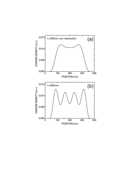
Fig. 2 shows the simulated charge density along the channel axis for the nanowire FET with nm. For comparison, the non-interacting case is shown in Fig. 2(a), whereas the realistic case which includes the Coulomb repulsion is plotted in Fig. 2(b). For this case, the single-particle quantization energy dominates as compared to the Coulomb repulsion, resulting in a charge distribution which resembles the shape of a non-interacting system. Here, the Coulomb repulsion solely broadens the spatial electron distribution. In contrast, for the nm case (Fig. 3(a) and (b)) one can clearly identify the formation of a charge density wave, indicating the onset of the Wigner molecule regime [17] with separated electrons owing to the dominating Coulomb repulsion. The actual transition to the Wigner regime for a nanowire FET in general results from a competition between kinetic energy and Coulomb energy, which of course depends on the chosen materials and geometries. In the long-channel case (nm), the mean spatial separation of the electrons becomes much larger than the screening length of the Coulomb interaction within the channel. For the discussed example, in turn, it is energetically favorable for the electrons to form a charge density wave in order to reduce the Coulomb energy, outweighing the increased kinetic energy due to the spatial confinement . Comparing the non-interacting case Fig. 3(a) with Fig. 3(b), one can clearly observe a qualitative change in the electron density profile.
In order to probe such a peculiar electronic configuration within a nanowire FET channel, we now consider the spatially resolved THz response spectrum of such a device. In the following simulation results, we have employed a resolution of 40 intermediate probe gates. One has to note that each individual gate finger detects a spatially averaged signal within an effective interval , where denotes the geometrical length of the gate segment and the gate screening length. Parasitic stray-capacitances which will likely occur in an experimental realization of such a device are not considered in this paper. For the experimental case it might be advantageous to employ alternating screening and signal gates, combined with an optimized THz layout.
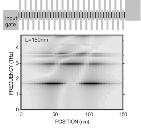
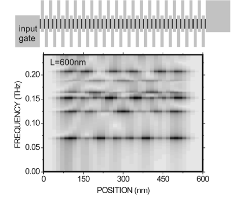
Fig. 4 and Fig. 5 show the simulated THz spectra for the two cases nm and nm, respectively, which exhibit fundamental resonances at 1.69THz and 70GHz. The higher value for the 150nm case stems from a narrower electron distribution (see Fig. 2(b)). Most noticeably, comparing the qualitative form of the two spectra, signatures of the Wigner-like regime for the 600nm case (Fig. 5) can be identified via the appearance of additional spatial peaks which are related to the oscillatory nature of the charge density wave. One has to note that the maxima in these transition spectra are located at those gate positions where the charge oscillates the most, and thus need not coincide with the charge density maxima. In fact, for a non-interacting case, the spatial THz pattern is related to the gate-averaged product of the two wavefunctions of the involved final and destination states [12]. Even with the inclusion of the electron-electron interaction, the considered nm device comes close to such a situation. In the case of a correlated many-body state, however, such an interpretation is not applicable in general and a many-body approach such as the BBCI becomes mandatory. In any case, the obtained THz spectra can be considered as “fingerprints” of the concrete electronic configuration of the channel, providing not only information about electronic transition energies but also about the spatial configuration of the underlying few-electron states.
IV Conclusion
In summary, we have considered a THz probe for a spatially resolved analysis of electronic spectra in nanowire-based transistors employing a multi-segment gate design. We have simulated the THz response of few-electron quantum states in nanowire FETs by use of a recently developed numerical many-body technique. The discussed example of a GaAs-based device demonstrates that signatures of Wigner-like charge density waves can be identified by use of this method, which lies beyond the scope of standard FET characterization methods. As such, the proposed multi-gate THz probe technique might prove useful in a future experimental realization as a means to characterize nanoscale devices which are dominated by quantization and Coulomb effects.
References
- [1] C. Thelander, T. Martensson, M.T. Björk, B.J. Ohlsson, M.W. Larsson, L.R. Wallenberg, and L. Samuelson, “Single-electron transistors in heterostructure nanowires”, Appl. Phys. Lett., vol. 83, no. 10, pp. 2052-2054, 2003.
- [2] J. Guo, S. Datta and M. Lundstrom, “A Numerical Study of Scaling Issues for Schottky Barrier Carbon Nanotube Transistors”, IEEE Trans. Electron Dev. , vol. 51, pp. 172, 2004.
- [3] K.M. Indlekofer, J. Knoch, and J. Appenzeller, “Quantum kinetic description of Coulomb effects in one-dimensional nanoscale transistors”, Phys. Rev. B, vol. 72, pp. 125308-1-7, 2005.
- [4] G.D. Vendelin, A.M. Pavio, and U.L. Rohde, “Microwave Circuit Design Using Linear and Nonlinear Techniques”, ISBN 0-471-60276-0, Wiley-Interscience, 1990.
- [5] R. Lake, G. Klimeck, R.C. Bowen, and D. Jovanovic, “Single and multiband modeling of quantum electron transport through layered semconductor devices”, J. Appl. Phys., vol. 81, no. 12, pp. 7845-7869, 1997.
- [6] D.L. John and D.L. Pulfrey, “Green’s Function Calculations for Semi-Infinite Carbon Nanotubes”, Physica Status Solidi (b), vol. 243, no. 2, pp. 442-448, 2006.
- [7] P.W. Anderson and A.M. Clogston, Bull. Am. Phys. Soc., vol. 6, pp. 124, 1961.
- [8] J. Hubbard, Proc. R. Soc., vol. A276, pp. 238, 1963.
- [9] K.M. Indlekofer, J. Knoch, and J. Appenzeller, “Quantum confinement corrections to the capacitance of gated one-dimensional nanostructures”, Phys. Rev. B, vol. 74, pp. 113310-113313, 2006.
- [10] K. M. Indlekofer, J. Knoch, and J. Appenzeller, cond-mat/0609025, accepted for publication in IEEE Trans. Eletron Dev., 2007.
- [11] K. M. Indlekofer and R. Németh, “Recursive approach to the calculation of a many-body basis in discrete electronic nanosystems”, cond-mat/0609540, 2006.
- [12] K. M. Indlekofer and R. Németh, to be published, 2007.
- [13] For a review see (and references therein): R. Dreizler and E. Gross, “Density Functional Theory”, Plenum Press, New York, 1995.
- [14] R. Kubo, “Statistical-Mechanical Theory of Irreversible Processes”, J. Phys. Soc. Jpn. vol. 12, pp. 570-586, 1957.
- [15] C.P. Auth and J.D. Plummer, “Scaling theory for cylindrical, fully-depleted, surrounding-gate MOSFET’s”, IEEE Electron Dev. Lett., vol. 18, no. 2 pp. 74-76, 1997.
- [16] C.W. Beenakker, “Theory of Coulomb-blockade oscillations in the conductance of a quantum dot”, Phys. Rev. B, vol. 44, no. 4, pp. 1646-1656, 1991.
- [17] W. Häusler and B. Kramer, “Interacting electrons in a one-dimensional quantum dot”, Phys. Rev. B, vol. 47, pp. 16353-16357, 1992.