A lattice of microtraps for ultracold atoms based on patterned magnetic films
Abstract
We have realized a two dimensional permanent magnetic lattice of Ioffe-Pritchard microtraps for ultracold atoms. The lattice is formed by a single 300 nm magnetized layer of FePt, patterned using optical lithography. Our magnetic lattice consists of more than 15000 tightly confining microtraps with a density of 1250 traps/mm2. Simple analytical approximations for the magnetic fields produced by the lattice are used to derive relevant trap parameters. We load ultracold atoms into at least 30 lattice sites at a distance of approximately 10 m from the film surface. The present result is an important first step towards quantum information processing with neutral atoms in magnetic lattice potentials.
pacs:
32.80.Pj, 39.25.+k, 03.67.LxI Introduction
Lattice potentials for ultracold neutral atoms and Bose-Einstein condensates have been used in a series of spectacular experiments. Optical lattices for example have allowed for the observation of the Mott-insulator to superfluid transition GreManEss02 , studies of low dimensional quantum gases ParWidHan04 ; HadKruDal06 and the coherent production of isolated and long lived cold molecules RomBesBlo04 ; StoMorEss06 ; ThaWinDen06 ; OspOspBon06 ; VolSyaRem06 . In another remarkable experiment large scale quantum entanglement ManGreBlo03 has been achieved in an optical lattice, pointing the way to future applications in quantum information processing.
Magnetic lattice potentials are a promising alternative to the widely used optical lattices that rely on intense overlapping laser beams. For instance, magnetic lattices produced using periodically magnetized films on atom chips provide a high degree of design flexibility allowing arbitrary trap geometries and lattice spacings GhaKieHan06 . The potentials are also magnetic state selective and only weak field seeking atoms remain trapped, allowing for manipulation using radio frequency (rf) fields - a powerful tool used extensively for forced evaporative cooling and for rf spectroscopy FerGerSpr07 . Furthermore, magnetic lattices provide stable and tight confinement even with large separation between sites. It should also be possible to incorporate on-chip detection and manipulation schemes TepLinVul06 to address individual sites.
Magnetic lattices may be most promising as a scalable quantum system, a crucial ingredient for quantum information processing Div00 . Trapped single atoms can be used as qubits, with their internal Zeeman or hyperfine states representing the qubit states and . Superpositions with a long coherence time have already been demonstrated near a chip surface TreHomRei04 , indicating that the coupling to environmental fields is weak.
In this paper we describe the design, fabrication and loading of a two-dimensional lattice of magnetic (Ioffe-Pritchard) microtraps for ultracold neutral atoms. The microtraps are produced near the surface of a patterned FePt film with perpendicular magnetization. Our magnetic lattice design consists of 1250 traps/mm2, with the expectation that this density can be scaled up by two or three orders of magnitude. We describe the properties of the magnetic film and our fabrication of the structure. Finally, we load a cloud of ultracold 87Rb atoms into this lattice, demonstrating that our approach is a feasible one. The results open up a range of new possibilities for future experiments using permanent magnetic atom chips.
The paper is structured as follows. In section II we present the lattice geometry based on a single layer of magnetised material which in combination with a uniform bias field produces a two-dimensional array of magnetic microtraps. We provide relatively simple analytical expressions to approximate the magnetic field patterns. In section III we describe the properties of the magnetic FePt films and our procedures for fabrication and patterning of the films. In section IV we show that ultracold 87Rb atoms can be transferred to the lattice from a Z-shaped wire magnetic trap, to occupy more than 30 lattice sites. Finally, we discuss some prospects for future experiments and in particular focus on quantum information processing using atom chips.
II A two-dimensional magnetic lattice potential
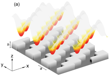
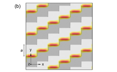
We have considered several geometries for producing magnetic lattices and have chosen a single design that produces an array of microtraps with non-zero field minima, provides tight confinement to the atoms and can be loaded in a straight-forward way. Our permanent magnetic lattice design is shown in Fig. 1. The magnetization is oriented out of the film plane (parallel to in Fig. 1b), and produces a field analogous to an array of Z-wire magnetic traps with an equivalent current of magnitude , where is the remanent magnetization and is the height of the magnetic film.
II.1 Magnetization model
The periodic magnetization pattern shown in Fig. 1 can be conveniently expressed as a two-dimensional Fourier series,
| (1) |
with the coefficients
| (2) |
Here, we choose a coordinate system such that the odd Fourier components vanish. The reciprocal lattice vectors and are given by and and have length and , respectively. We define and is a characteristic length scale of the lattice geometry as shown in Fig. 1. As the magnetization is simply the sum of a number of discrete Fourier components the magnetic field above the surface can be expressed analytically. For each Fourier component with wavevector and for the magnetic scalar potential is given by:
| (3) |
The magnetic field () above the film surface can be approximated by taking ={-1,0,1}, leaving two terms:
| (4) |
where the approximation is valid for distances . Each field component consist of two periodic terms with exponential prefactors which depend on and control the respective rate of decay of each Fourier component from the film surface. For large distances from the film surface the first term with wave vector dominates and the field resembles that of a one-dimensional magnetic mirror potential HinHug99 . Closer to the surface the second term involving introduces additional structure to produce a two-dimensional periodic potential.
Applying a uniform bias magnetic field oriented along the direction partly cancels with the field of the film to create an array of nonzero field minima. The applied field strength is related to the trap height by,
| (5) |
while the trap positions in and are given by symmetry and are independent of height:
| (6) |
with the indices .
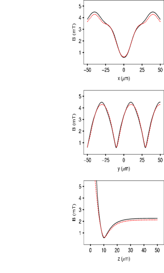
Our particular design has a length scale m, a magnetization of = 670 kA/m and a thickness of nm, corresponding to A. We calculate that a bias field of mT results in cigar-shaped Ioffe-Pritchard traps, with their long axis predominantly oriented in the -direction, positioned 10 m from the film surface (Fig. 2). The trapping frequencies are 23 kHz and 6.1 kHz in the radial and axial directions respectively and the field strength at the trap minimum is 0.57 mT. The barrier heights along the and directions are 0.4 mK and 1.5 mK, respectively. The trap depth in the -direction is 1.5 mK. The trapping frequencies can be increased further by increasing , pushing the atoms closer to the chip surface. Tighter radial confinement can also be achieved by partly cancelling the axial field strength. The barrier height between individual lattice sites can be tuned by varying to change the distance of the traps from the film surface.
III FePt magnetic films
Magnetic materials used for experiments with ultracold atoms and Bose-Einstein condensates should be magnetically hard with a magnetization sufficient to produce the field strength and gradients for providing tight confinement to the atoms SinCurHin05 ; HalWhiSid06 ; BoyStrPri06 ; FerGerSpr07 . They should also have a high coercivity in order to maintain the magnetization when subjected to externally applied fields. The magnetization should be oriented perpendicular to the film surface to give maximal design freedom and should be highly homogeneous to allow for intricate magnetic field designs and to avoid unwanted spatial variations of the magnetic field WhiHalSid07 . Other desired properties include high corrosion resistance to facilitate lithographic patterning and good temperature stability especially during vacuum bake out.
A suitable magnetic material for these experiments is FePt XiaBruBus04 ; WeiSchFah04 ; YanPowSel02 . Films of FePt have a high remanent magnetization XinBarGerPP , are extremely stable and corrosion resistant which allows patterning on the micron scale using conventional photolithographic techniques. FePt can be created in several phases. The face centered cubic (fcc) phase is magnetically soft but has a high saturation magnetization =1160 kA/m. The ordered face centered tetragonal phase (fct), in which Fe and Pt atomic layers are stacked along the (001) direction, is magnetically hard with high uniaxial anisotropy constant MJ/m3.

III.1 Film preparation and characterisation
We investigated two preparation methods for producing FePt films. The first set was prepared at the Hitachi San Jose Research Center. The films are deposited on 300 m thick silicon substrates coated with approximately 10 nm of SiN by magnetron sputter deposition at a temperature of C. The films incorporate a 10 nm thick amorphous CrTi underlayer and a seed layer of 10 nm RuAl used to directly grow the FePt in the fct phase in the (001) direction SheJudWan05 . The FePt layer itself was doped with a small amount (10 at.%) of carbon to increase the remanent to saturation magnetization ratio. Evidence for the textured nature of the film was obtained from x-ray diffraction spectra.
The magnetization of the films were measured by vibrating sample magnetometry yielding a remanent magnetization of 670 kA/m, a remanent to saturation magnetization ratio of 0.93 and a coercivity of 0.95 T. Figure 3 shows a hysteresis curve of a 200 nm thick film. There were no significant differences between films of various thickness in the range 200-400 nm.
To test the suitability of our FePt films for atom optics applications we magnetize and then bake the deposited films for 3 hours at 150 ∘C in air to characterize temperature stability. After baking the magnetization had reduced by 3 . The films were also tested against demagnetization due to time varying magnetic fields. An experimental cycle typically involves external fields of up to 20 mT with a cycle time of about 30 s. To test the stability of the magnetization in those fields the films were magnetized and minor hysteresis loops were taken over the range of -20 mT to 20 mT. The magnetization did not measurably decrease after 15 cycles. Additional long-term tests performed within the experimental apparatus also indicate the magnetization is stable during typical experimental cycles.
We have also measured the surface roughness and grain size of the films using atomic force microscopy, scanning electron microscopy and x-ray diffraction. Surface roughness can be a significant source of spatial magnetic field noise. The rms height variation in the film is 6 nm. The grain size is related to the width of the x-ray diffraction peaks via the Debye Scherrer equation. This yields an average grain size of 35 nm. Taking these numbers into account we anticipate spatial magnetic field variations around 0.4 T which corresponds to energy variations between lattice sites of less than the vibrational level spacing ( 6 kHz) WhiHalSid07 .
As a second route to produce hard magnetic FePt films we investigated the possibility of rapid post annealing of films magnetron sputtered directly onto silicon at lower temperatures (250∘C). After deposition at this temperature the FePt is in a highly disordered partly amorphous fcc soft magnetic phase. The film is annealed at a temperature of 450∘C for 3 minutes in order to initiate the hard magnetic fct phase. This film had a remanent magnetization of 580 kA/m, a remanent to saturation magnetization ratio of 0.80 and a coercivity of 0.95 T. Although the magnetization is somewhat smaller than for the first film the post annealed film has the advantage that it has a smaller surface roughness (1 nm rms height variation) and smaller grains ( 20 nm diameter). Furthermore, the annealed film is straightforward to produce without the complication of underlayers. It was however less stable against elevated temperatures and showed a 20 % decrease in magnetization after a 3 hour 150 ∘C bake, persuading us to use the Hitachi film for the experiment.
III.2 Patterning
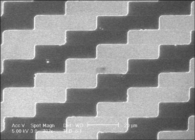
To pattern our films we use optical lithography. We used a commercially obtained custom designed Cr mask. This mask was patterned with a 442 nm HeCd laser with a resolution of m. The deposited films are first spin coated with m optical resist and then illuminated for 4 s using a I-line (365 nm) mask aligner. After developing the samples for one minute the resist on the illuminated parts of the sample is dissolved. The surface can be cleaned with a low power, two minute oxygen etch using a dry etching system. The exposed FePt surface was then etched using an argon plasma for about 30 minutes. The remaining resist covering the chip structures was then removed in an ultrasonic bath. After this the chip was investigated using optical and scanning electron microscopy (SEM). A SEM image of the lattice is shown in Fig. 4. Finally, the magnetic films were coated with a 100 nm reflective gold over layer and were magnetized in a 5 T magnetic field.
III.3 Chip construction
The completed atom chip consists of the silicon substrate with the patterned FePt film epoxied to a copper mount which incorporates a wire structure used to load the microtraps (Fig. 5). In particular, the atom chip includes (besides the FePt film) a U-shaped wire, a Z-shaped wire and a small rf coil (ten turns, diameter 5 mm) used to apply radio frequency fields for forced evaporative cooling. The chip wires are m wide, have a height of m and are capable of running up to 15 A continuously without significant heating. The atom chip is mounted face-down in a glass cell vacuum chamber, surrounded by a system of three orthogonal pairs of coils for producing external fields FerGerSpr07 .
IV Loading atoms to the lattice potential
Laser cooled 87Rb atoms are transferred to the atom chip using techniques common to many atom chip experiments. After an initial cooling stage the atoms can be transferred to the magnetic lattice potential. The following section describes the loading process.
IV.1 Magnetic trapping and evaporative cooling
We collect approximately 87Rb atoms in a mirror magneto optical trap (mMOT) 4 mm from the chip surface. This mMOT relies on a quadrupole magnetic field (0.1 T/m) produced by a pair of external coils overlapped with four laser beams with appropriate detuning and polarizations.
The atoms are transferred closer to the chip by passing 5.5 A through the U-shaped wire, applying a bias field of mT, and ramping off the external magnetic quadrupole field. This U-MOT has a field gradient of 0.2 T/m. To further cool the atoms a 4 ms polarisation gradient cooling stage is applied by detuning the trap laser below resonance by 36 MHz and rapidly reducing the U-wire current and bias field by a factor of three to weaken the field gradient. We found that this stage significantly improves the loading efficiency into the magnetic trap. To magnetically trap the atoms a 0.2 ms optical pumping pulse in a uniform magnetic field drives the atoms to the state. Then the U-wire current is reduced to zero, the Z-wire current is increased to 12 A and the bias field is increased to 1.4 mT to produce an Ioffe-Pritchard magnetic trap containing atoms. We then adiabatically compress the trap by increasing the Z-wire current to 15 A and by increasing to 4.0 mT. The calculated radial and axial trap frequencies are Hz and Hz respectively. The mean elastic collision rate is s-1.
Forced RF evaporative cooling is applied by a programmable DDS rf synthesiser via a 2 W rf amplifier to the built-in rf coil. The evaporation stage consists of three linear rf sweeps: from 15 MHz to 6 MHz in 2.5 s, from 6 MHz to 3 MHz in 1.5 s and from 3 MHz to the final evaporation frequency of 520 kHz in a further 2 s. To improve the evaporation efficiency we also compress the Z-wire trap further after the first sweep by increasing to 5.0 mT which pushes the trap closer to the surface and increases the radial trap frequency to Hz. For a final radio frequency of 545 kHz the cloud temperature reaches the Bose-Einstein condensation (BEC) temperature (K) with approximately atoms. The BEC transition is accompanied by the onset of a bimodal density distribution and anisotropy in the time of flight expansion. Continuing the rf sweep to 520 kHz we produce an almost pure BEC containing 6000 atoms.
IV.2 Transfer to the lattice
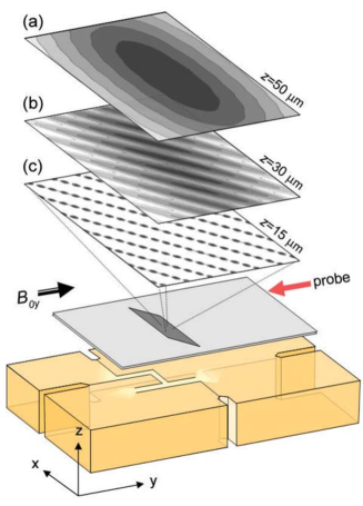
To load atoms to the lattice we truncate the rf sweep at a final frequency of 800 kHz to produce a cold thermal cloud of atoms at an estimated temperature of K. We load the lattice with a thermal cloud rather than a Bose-Einstein condensate to ensure each lattice site contains a sufficient number of atoms for detection and to minimise the influence of heating during loading. We expect that further rf evaporation could be performed after loading with high efficiency due to the extremely tight confinement in individual lattice sites. Loading the lattice is rather straightforward as the magnetic field produced by each lattice site is by design oriented in the same direction as that produced by the Z-shaped wire. In this way we can simply reduce the Z-wire current to zero, pushing the trapped atoms closer to the surface and finally into the lattice potential. The atoms are imaged using a resonant probe laser aligned along with a small inclination () with respect to the chip surface to produce a reflection image. Reflection imaging allows us to image atom clouds in close proximity to the chip surface and to determine the height of the cloud. One disadvantage however is that the absorption signal is integrated along the direction.
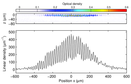
In the experiment we reduce the Z-wire current from 15 A to zero over 50 ms to move the trap closer to the FePt film. For a Z-wire current of 2 A the cloud expands in the axial direction, moves to approximately m from the FePt surface and becomes clearly corrugated by the lattice potential, as is schematically shown in Fig. 5. Further decreasing the Z-wire current to zero transfers all of the atoms to the magnetic lattice (Fig. 6). The spacing between lattice sites determined from an absorption image of the cloud is m, as expected from the lattice geometry. The overall gaussian density distribution is due to the initial distribution of atoms in the Z-wire trap and does not expand further after loading. We observe a minimum of 30 occupied lattice sites spanning m along but the true number of occupied sites may be higher. A better estimate of the number of occupied lattice sites may be obtained in the future by inclining the probe beam further to resolve the lattice structure along the axis. Assuming adiabatic compression during loading we expect the individual atom clouds to be localized, each at a temperature of K, smaller than the inter-well barrier height and trap depth ( mK). We observe a lifetime of more than 1 s for the atoms trapped in the lattice potential.
V Discussion
Our present observation shows clouds of trapped atoms spaced by 20 m along the -direction. It is likely that at least a few sites are occupied along the detection direction. Large arrays of microtraps can serve as a quantum register and a shift register DotAltRau05 ; BeuTucGra07 . Field calculations show that we should be able to shift the traps in the direction perpendicular to by applying uniform external -fields GerSpr06 ; HinHug99 .
The present density of lattice sites is 1250 traps/mm2. It should be feasible to scale down the linear dimensions of our structure into the (sub-)micron range and thus increase the trap density by two or three orders of magnitude. We are presently investigating the possibilities to drive single and two-qubit gate operations CalHinZol00 . We plan to directly address individual sites by a combination of static and radio frequency or microwave fields, to selectively change the internal state of the atoms. An important parameter for the optical manipulation of the qubits is the confinement of the atoms on the scale of the optical wavelength. The present confinement is already sufficiently tight for the trap ground state to be in the so-called Lamb-Dicke limit, where the photon recoil energy is less than the vibrational level splitting. Further downscaling in size should make the confinement even tighter, and thus decrease the Lamb-Dicke parameter. We plan to implement rf evaporative cooling in the lattice to produce ground state atoms in every lattice site. Together these implementations will be important first steps towards future quantum information processing applications on atom chips TreSteHan06 .
To summarize, we described the design and production of a permanent magnetic array of Ioffe-Pritchard microtraps for cold atoms based on FePt. We have given analytical expressions for the magnetic field produced by this lattice. We have investigated magnetic films for producing the lattice. We have loaded more than 30 lattice sites with cold atoms. The loading protocol relies on current carrying structures beneath the permanent magnetic chip. The lifetime of the atoms trapped in the lattice exceeds 1 s.
Acknowledgements.
We gratefully acknowledge technical support from Chris Rétif and Huib Luigjes. This work is part of the research program of the Stichting voor Fundamenteel Onderzoek van de Materie (Foundation for the Fundamental Research on Matter) and was made possible by financial support from the Nederlandse Organisatie voor Wetenschappelijk Onderzoek (Netherlands Organization for the Advancement of Research) and by the fabrication and characterization facilities of the Amsterdam nanoCenter. It was also supported by the EU under contract MRTN-CT-2003-505032.References
- (1) M. Greiner et al., Nature 415, 39 (2002).
- (2) B. Paredes et al., Nature 429, 277 (2004).
- (3) Z. Hadzibabic et al., Nature 5, 441 (2006).
- (4) T. Stöferle et al., Phys. Rev. Lett. 96, 030401 (2006).
- (5) T. Rom et al., Phys. Rev. Lett. 93, 073002 (2004).
- (6) G. Thalhammer et al., Phys. Rev. Lett. 96, 050402 (2006).
- (7) C. Ospelkaus et al., Phys. Rev. Lett. 97, 120402 (2006).
- (8) T. Volz et al., Nature Phys. 2, 692 (2006).
- (9) O. Mandel et al., Nature 425, 937 (2003).
- (10) S. Ghanbari, T. D. Kieu, A. Sidorov, and P. Hannaford, J. Phys. B: At. Mol. Opt. Phys. 39, 847 (2006).
- (11) T. Fernholz et al., arXiv:0705.2569 (2007).
- (12) I. Teper, Y.-J. Lin, and V. Vuletić, Phys. Rev. Lett. 97, 023002 (2006).
- (13) D. P. DiVincenzo, Fortschr. Phys. 48, 771 (2000).
- (14) P. Treutlein et al., Phys. Rev. Lett. 92, 203005 (2004).
- (15) E. A. Hinds and I. G. Hughes, J. Phys. D: Appl. Phys. 32, R119 (1999).
- (16) C. D. J. Sinclair et al., Phys. Rev. A 72, 031603(R) (2005).
- (17) B. V. Hall et al., J. Phys. B: At. Mol. Opt. Phys. 39, 27 (2006).
- (18) M. Boyd et al., arXiv:cond-mat/0608370 (2006).
- (19) S. Whitlock et al., Phys. Rev. A 75, 043602 (2007).
- (20) Q. Xiao et al., J. All. Comp. 364, 315 (2004).
- (21) M. Weisheit, L. Schultz, and S. Fähler, J. Appl. Phys. 95, 7489 (2004).
- (22) M. L. Yan, N. Powers, and D. J. Sellmyer, J. Appl. Phys. 93, 8292 (2002).
- (23) Y. T. Xing et al., J. Magn. Magn. Mater. 313, 192 (2007).
- (24) W. K. Shen, J. H. Judy, and J.-P. Wang, J. Appl. Phys. 97, 10H301 (2005).
- (25) I. Dotsenko et al., Phys. Rev. Lett. 95, 033002 (2005).
- (26) J. Beugnon et al., arXiv:0705.0312 (2007).
- (27) R. Gerritsma and R. J. C. Spreeuw, Phys. Rev. A 74, 043405 (2006).
- (28) T. Calarco et al., Phys. Rev. A 61, 022304 (2000).
- (29) P. Treutlein et al., Fortschr. Phys. 54, 702 (2006).