Interband, intraband and excited-state direct photon absorption of silicon and germanium nanocrystals embedded in a wide band-gap lattice
Abstract
Embedded Si and Ge nanocrystals (NCs) in wide band-gap matrices are studied theoretically using an atomistic pseudopotential approach. From small clusters to large NCs containing on the order of several thousand atoms are considered. Effective band-gap values as a function of NC diameter reproduce very well the available experimental and theoretical data. It is observed that the highest occupied molecular orbital for both Si and Ge NCs and the lowest unoccupied molecular orbital for Si NCs display oscillations with respect to size among the different irreducible representations of the point group to which these spherical NCs belong. Based on this electronic structure, first the interband absorption is thoroughly studied which shows the importance of surface polarization effects that significantly reduce the absorption when included. This reduction is found to increase with decreasing NC size or with increasing permittivity mismatch between the NC core and the host matrix. Reasonable agreement is observed with the experimental absorption spectra where available. The deformation of spherical NCs into prolate or oblate ellipsoids are seen to introduce no pronounced effects for the absorption spectra. Next, intraconduction and intravalence band absorption coefficients are obtained in the wavelength range from far-infrared to visible region. These results can be valuable for the infrared photodetection prospects of these NC arrays. Finally, excited-state absorption at three different optical pump wavelengths, 532 nm, 355 nm and 266 nm are studied for 3- and 4 nm-diameter NCs. This reveals strong absorption windows in the case of holes and a broad spectrum in the case of electrons which can especially be relevant for the discussions on achieving gain in these structures.
pacs:
73.22.-f, 78.67.Bf, 78.40.-qI Introduction
The field of silicon and germanium nanocrystals (NCs) is very active due to important technological achievements and prospects particularly in connection with optics such as light emitting diodes and lasers.ossicini ; pavesi00 ; walters ; rong Two fundamental processes describing the interaction of light with matter are the photon absorption and emission. In the context of NCs, it has been shown both experimentally wolkin and theoretically zhou ; luppi that the interface properties have dramatic effects on the emission properties. On the other hand, absorption measurements are less sensitive to surface quality and allow for a more direct characterization of the intrinsic structure of NCs.sagnes Therefore, the study of the direct photon absorption in NCs can provide a clear physical understanding. Moreover, with the ever-growing importance of renewable energy resources, the research on the new-generation photovoltaics has gained momentum and hence the subject of direct photon absorption in nanocrystalline silicon (-Si).pv However, both experimentally furukawa ; kanemitsu ; takeoda ; wilcoxon99 ; kovalev ; wilcoxon01 and theoretically, vasiliev ; weissker02a ; weissker02b ; weissker03 ; ramos ; melnikov ; tsolakidis ; trani05 researchers till now have predominantly focused on the interband absorption process. This is the only optical absorption possibility for an intrinsic semiconductor NC under equilibrium. By relaxing these two constraints we can introduce other absorption channels, mainly through carrier injection or optical pumping. The associated absorption in either case is sometimes referred to as “free” carrier absorption despite the carrier confinement in NCs. In our work we discriminate between the two. The electrical injection or doping gives rise to intraband absorption, also termed as intersubband absorption lin which has practical importance for mid- and near-infrared photodetectors.qdip The optical pumping which is usually well above the effective band gap leads to excited-state absorption (also termed as photoinduced absorption) which is an undesired effect that can inhibit the development of optical gain.malko Recent experiments on excited-state absorption concluded that more attention should be devoted to the role of the excitation conditions in the quest for the silicon laser.elliman ; trojanek ; forcales Therefore, the aim of this work is to provide a comprehensive theoretical account of all of these direct photon absorption mechanisms in Si and Ge NCs under various size, shape and excitation conditions. This provides a complementary track to the existing experimental efforts where the size and shape control are currently major obstacles.
The absorption coefficient of the semiconductor NCs depends on the product of the optical transition oscillator strength and their joint density of states as well as to their volume filling factor within the matrix. Therefore, the essential decision on a theoretical study is the sophistication level of the electronic structure. The usual trade off between the computational cost and accuracy is operational. The constraints on the former are quite stringent as a NC including the active region of the matrix surrounding itself can contain on the order of ten thousand atoms. As for the latter, not only the accuracy but also the validity of a chosen approach can become questionable. Computationally low-cost approaches like the envelope function in conjunction with 8-band kp are not as accurate for this task and furthermore, they miss some critical symmetries of the underlying lattice. zunger On the other extreme, there lies the density functional theory-based ab initio codes martin-book which have been applied to smaller NCs containing less than 1000 atoms which still require very demanding computational resources. ogut ; weissker02a ; weissker02b ; weissker03 ; ramos ; luppi ; melnikov ; tsolakidis The ab initio analysis of larger NCs of sizes between 3-10 nm is practically not possible with the current computer power. While this technological hurdle will be gradually overcome in the years to come, there exists other atomistic approaches that can be employed for NC research which can be run on modest platforms and are much simpler to develop, such as the tight binding technique which has been successfully employed by several groups. delerue04 ; ren ; niquet ; trani05 On the pseudopotential-based approaches, two new recipes were proposed by Wang and Zunger over the last decade. wang94a ; wang97 ; wang99 The folded spectrum method wang94a relies on standard plane wave basis and direct diagonalization; its speed is granted from being focused on relatively few targetted states. For the study of excitons this approach becomes very suitable whereas for the optical absorption spectra where a large number of states contribute it loses its advantage. Their other recipe is the so-called linear combination of bulk bands (LCBB). wang94a ; wang97 ; wang99 As a matter of fact, the idea of using bulk Bloch states in confined systems goes back to earlier times, one of its first implementations being the studies of Ninno et al. ninno85 ; ninno86 Up to now, it has been used for self-assembled quantum dots, wang97 ; wang99 superlattices, botti01 ; botti04 and high-electron mobility transistors, chirico and very recently on the -Si aggregation stages. bulutay07 In this work, we apply LCBB to the electronic structure and absorption spectra of Si and Ge NCs. An important feature of this work, in contrast to commonly studied hydrogen-passivated NCs is that we consider NCs embedded in a wide band-gap matrix which is usually silica. pecvd In principle, other matrices such as alumina or silicon nitride can be investigated along the same lines.
The organization of the paper is as follows: in Section II we describe the theoretical framework which includes some brief information on the LCBB technique and the absorption expressions. A self-critique of the theoretical model is done in Section III. Section IV presents the results and discussions on the band edge electronic structure, interband, intraband, and excited-state absorptions followed by our conclusions in Section V. Appendix section contains technical details on the employed pseudopotential form factors and our LCBB implementation.
II Theory
For the electronic structure of large-scale atomistic systems Wang and Zunger have developed the LCBB method which is particularly convenient for embedded NCs containing several thousand atoms. wang97 ; wang99 The fact that it is a pseudopotential-based method makes it more preferable over the empirical tight binding technique for the study of optical properties as aimed in this work. In this technique the NC wavefunction with a state label is expanded in terms of the bulk Bloch bands of the constituent core and/or embedding medium (matrix) materials
| (1) |
where is the number of primitive cells within the computational supercell, is the expansion coefficient set to be determined and is the constituent bulk material label pointing to the NC core or embedding medium. is the cell-periodic part of the Bloch states which can be expanded in terms of the reciprocal lattice vectors as
| (2) |
where is the volume of the primitive cell. The atomistic Hamiltonian for the system is given by
| (3) |
where is the weight function that takes values 0 or 1 depending on the type of atom at the position , note1 and is the screened spherical pseudopotential of atom of the material . We use semiempirical pseudopotentials for Si and Ge developed particularly for strained Si/Ge superlattices which reproduces a large variety of measured physical data such as bulk band structures, deformation potentials, electron-phonon matrix elements, and heterostructure valence band offsets. friedel With such a choice, this approach benefits from the empirical pseudopotential method (EPM), which in addition to its simplicity has another advantage over the more accurate density functional ab initio techniques that run into well-known band-gap problem martin-book which is a disadvantage for the correct prediction of the excitation energies.
| (4) |
where
Here, the atoms are on regular sites of the underlying Bravais lattice: where are its direct lattice vectors of the Bravais lattice. Both the NC and the host matrix are assumed to possess the same lattice constant and the whole structure is within a supercell which imposes the periodicity condition , recalling its Fourier representation , implies , so that , where are the reciprocal lattice vectors of the bulk material. Thus the reciprocal space of the supercell arrangement is not a continuum but is of the grid form composed of points , where .
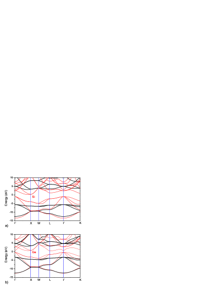
An important issue is the choice of the host matrix material. If the NC is surrounded by vacuum, this corresponds to the free-standing case. However, the dangling bonds of the surface NC atoms lead to quite a large number of interface states which adversely contaminate especially the effective band-gap region of the NC. In practice NCs are embedded into a wide band-gap host matrix which is usually silica. pecvd However, the pseudopotential for oxygen is nontrivial in the case of EPM chelikowsky77 and furthermore, lattice constant of SiO2 is not matched to either of the core materials introducing strain effects. Therefore, we embed the Si and Ge NCs into an artificial wide band-gap medium which for the former reproduces the proper band alignment of the Si/SiO2 system. To circumvent the strain effects which are indeed present in the actual samples, we set the lattice constant and crystal structure of the matrix equal to that of the core material. The pseudopotential form factors of the wide band-gap matrices for Si and Ge can easily be produced starting from those of the core materials. More details are provided in the Appendix section. The resultant bulk band structures for Si and Ge and their host wide band-gap matrices are shown in Fig. 1. With the use of such a lattice-matched matrix providing the perfect termination of the surface bonds of the NC core atoms lead to the removal of all gap states as can be observed in Fig. 2. In these plots, the evolution of the effective band-gaps towards their bulk values (marked by dashed lines) is clearly seen as the diameter increases.

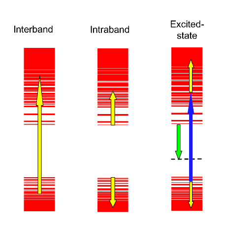
Once the electronic wavefunctions of the NCs are available, their linear optical properties can be readily computed. The three different types of direct (zero-phonon) photon absorption processes considered in this work are illustrated in Fig. 3. These are interband, intraband and excited-state absorptions. In the latter, the blue (dark-colored) arrow represents optical pumping and following carrier relaxation, the downward green arrow corresponds to luminescence which can be to a final interface state (dashed line). pavesi00 For all these processes, the relevant quantity is the imaginary part of the dielectric function. Within the independent-particle approximation and the artificial supercell framework weissker02a it becomes
| (5) | |||||
where, denotes the cartesian components of the dielectric tensor and
| (6) |
is the oscillator strength of the transition. In these expressions is the free electron mass, is the magnitude of the electronic charge, and is the full-width at half maximum value of the Lorentzian broadening. The label () correspond to occupied (empty) valence (conduction) states referring only to their orbital parts in the absence of spin-orbit coupling; the spin summation term is already accounted in the prefactor of Eq. 5. Finally, is the volume of the supercell which is a fixed value chosen conveniently large to accommodate the NCs of varying diameters, however, if one uses instead, that of the NC, , this corresponds calculating where is the volume filling ratio of the NC. For the sake of generality, this is the form we shall be presenting our results. The electromagnetic intensity absorption coefficient is related to the imaginary part of the dielectric function through jackson
| (7) |
where is the index of refraction and is the speed of light.
In the case of intraband absorption, its rate depends on the amount of excited carriers. Therefore, we consider the absorption rate for one excited electron or hole that lies at an initial state with energy . As there are a number of closely spaced such states, we perform a Boltzmann averaging over these states as . We further assume that the final states have no occupancy restriction, which can easily be relaxed if needed. The expression for absorption rate per an excited carrier in each NC becomes
| (8) | |||||
where again is the light polarization direction.
Finally, we include the surface polarization effects, also called local field effects (LFE) using a simple semiclassical model which agrees remarkably well with more rigorous treatments. trani07 We give a brief description of its implementation. First, using the expression
| (9) |
we extract (i.e., de-embed) the size-dependent NC dielectric function, , where corresponds to Eq. 5, suppressing the cartesian indices. is the dielectric function of the host matrix; for simplicity we set it to the permittivity value of SiO2, i.e., . Since the wide band-gap matrix introduces no absorption up to an energy of about 9 eV, we can approximate . One can similarly obtain the within the random-phase approximation, trani05 hence get the full complex dielectric function . According to the classical Clausius-Mossotti approach, which is shown to work also for NCs, mahan the dielectric function of the NC is modified as
| (10) |
to account for LFE. The corresponding supercell dielectric function, follows using Eq. 9. Similarly, the intensity absorption coefficients are also modified due to surface polarization effects, cf. Eq. 7. Its consequences will be reported in Section IV.
III A self-critique of the theoretical model
The most crucial simplification of our model is the fact that strain-related effects are avoided, a route which is shared by other theoretical works. delley ; weissker02a ; weissker02b ; niquet ; trani05 For large NCs this may not be critical, however, for very small sizes this simplification is questionable. An important support for our act is that Weissker and coworkers have concluded that while there is some shift and possibly a redistribution of oscillator strengths after ionic relaxation, the overall appearance of the absorption spectra does not change strongly. weissker03 We should mention that Wang and Zunger have offered a recipe for including strain within the LCBB framework, however, this is considerably more involved. wang99 Another widespread simplification on Si and Ge NCs is the omission of the spin-orbit coupling and the nonlocal (angular momentum-dependent) pseudopotential terms in the electronic structure Hamiltonian. Especially the former is not significant for Si which is a light atom but it can have a quantitative impact on the valence states of Ge NCs; such a treatment is available in Ref. reboredo01, .
On the dielectric response, there are much more sophisticated and involved treatments onida whereas ours is equivalent to the independent particle random phase approximation ehrenreich of the macroscopic dielectric function with the surface polarization effects included within the classical Clausius-Mossotti model. trani07 The contribution of the excluded excitonic and other many-body effects beyond the mean-field level can be assessed a posteriori by comparing with the available experimental data. However, it is certain that the precedence should be given to classical electrostatics for properly describing the background dielectric mismatch between the core and the wide band-gap matrix. trani07 In our treatment this is implemented at an atomistic level.
Another effect not accounted in this work is the role of the interface region. Our wide band-gap matrix can reproduce the proper band alignment and dielectric confinement of an SiO2 matrix, however, the interface chemistry such as silicon-oxygen double bonds luppi are not represented. These were shown to be much more effective on the emission spectra. zhou ; luppi Nevertheless, our results can be taken as the benchmark for the performance of the atomistic quantum and dielectric confinement with a clean and inert interface. Finally, we do not consider the phonon-assisted hybertsen or nonlinear absorption. The list of these major simplifications also suggest possible improvements of this work.
IV Results and discussions
In this section we present our theoretical investigation of the linear optical properties of Si and Ge NCs. Three different direct photon absorption processes are considered as illustrated in Fig. 3 each of which can serve for technological applications as well as to our basic understanding. However, we first begin with the dependence of the optical gap on the NC size, mainly as a check of our general framework. There exist two different atomic arrangements of a spherical NC depending on whether the center of the NC is an atomic position or a tetrahedral interstitial location; under no ionic relaxation, Delley and Steigmeier have treated both of these classes as having the point symmetry. delley However, the tetrahedral interstitial-centered arrangement should rather have the lower point symmetry of and it is the arrangement that we construct our NCs. This leads to even number of NC core atoms, whereas it becomes an odd number with the point symmetry. We identify the irreducible representation of a chosen NC state by checking its projection to the subspace of each representation. reboredo00 For the point group these are denoted by , , and . We utilize this group-theoretic analysis in the next subsections.
IV.1 Effective optical gap
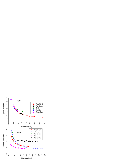
The hallmark of quantum size effect in NCs has been the effective optical gap with quite a number of theoretical wang94b ; ogut ; vasiliev ; garoufalis ; tsolakidis ; trani05 and experimental kanemitsu ; takeoda ; wilcoxon99 ; wilcoxon01 studies performed within the last decade. Figure 4 contains a compilation of some representative results. For Si NCs, it can be observed that there is a good agreement among the existing data, including ours. On the other hand, for the case of Ge NCs there is a large spread between the experimental data whereas our theoretical results are in very good agreement with both ab initio tsolakidis and tight binding results. trani05 In our approach the optical gap directly corresponds to the LUMO-HOMO energy difference, as calculated by the single-particle Hamiltonian in Eq. (3). This simplicity relies on the finding of Delerue and coworkers that the self-energy and Coulomb corrections almost exactly cancel each other for Si NCs larger than a diameter of 1.2 nm. delerue00
IV.2 HOMO and LUMO oscillations with respect to size
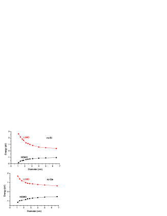
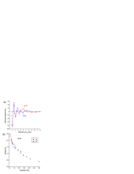
When we plot the variation of individual LUMO and HOMO levels as in Fig. 5 we observe with the exception of -Ge LUMO curve some non-smooth behavior that gets pronounced towards smaller sizes. The triple degeneracy in the absence of spin-orbit coupling of the valence band maximum in bulk Si and Ge is lifted into two degenerate and one nondegenerate states. The energy difference between these two set of states is observed to display an oscillatory behavior as the NC size gets smaller as shown in Fig. 6 (a). Using the point group symmetry operations we identify the doubly degenerate states to belong to representation and nondegenerate state to or . Furthermore, we observe a similar oscillation in the LUMO region of Si NCs as shown in Fig. 6(b). The low-lying conduction states of Si NCs form six-pack groups which is inhereted from the six equivalent 0.85X conduction band minima of bulk Si. The confinement marginally lifts the degeneracy by sampling contributions from other parts of the Brillouin zone. This trend is observed in Fig. 6(b) as the NC size gets smaller. On the other hand, for Ge NCs all LUMO states belong to the same representation and therefore shows no oscillations (cf. Fig. 5). Ultimately, the source of these oscillations is the variation of the asphericity of the NCs of point symmetry with respect to size, which can energetically favor one of the closely spaced states. In the case of the LUMO state of Ge NCs, there is a substantial energy gap between LUMO and the next higher-lying state.
| nc-Si | nc-Ge | |||||
|---|---|---|---|---|---|---|
| (nm) | HOMO | LUMO | (nm) | HOMO | LUMO | |
| 32 | 1.06 | 1.11 | ||||
| 38 | 1.13 | 1.18 | ||||
| 56 | 1.29 | 1.34 | ||||
| 74 | 1.41 | 1.47 | ||||
| 86 | 1.49 | 1.55 | ||||
| 116 | 1.64 | 1.71 | ||||
| 130 | 1.71 | 1.78 | ||||
| 136 | 1.73 | 1.80 | ||||
| 190 | 1.94 | 2.01 | ||||
| 264 | 2.16 | 2.25 | ||||
| 384 | 2.45 | 2.55 | ||||
| 522 | 2.71 | 2.82 | ||||
| 690 | 2.98 | 3.10 | ||||
| 768 | 3.08 | 3.21 | ||||
| 1702 | 4.02 | 4.18 |
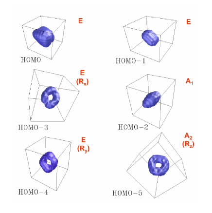
For further insight, we display in Fig. 7 the isosurface plots of the envelope of the six highest states up to HOMO for a Si NC of diameter 2.16 nm. Point group representation of each state is also indicated. For this particular diameter, HOMO has representation which is twofold degenerate. The nondegenerate state also becomes the HOMO for different diameters. This is illustrated in Table I which shows the evolution of the HOMO and LUMO symmetries as a function of diameter for Si and Ge NCs. There, it can be observed that for the latter the HOMO can also acquire the for larger diameters.
IV.3 Interband absorption
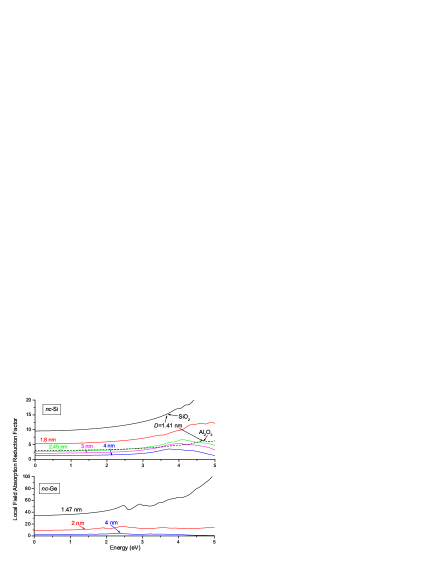
The interband absorptions of Si and Ge NCs for a variety of diameters are shown in Fig. 8. For a fair comparison, all different size NCs should possess the same volume filling factor. Therefore, we display the results at unity volume filling or equivalently per .weissker02b The left and right panels display the cases without and with surface polarization effects (or LFE), respectively. There exists remarkable differences between the two for both Si and Ge NCs. For instance, even though Ge NCs do not show significant size dependence without LFE, this is not the case when LFE is included. From the ratio of both panels, the so-called local field absorption reduction factor can be extracted as shown in Fig. 9. It can be observed that its size dependence is much stronger than the energy dependence. This reduction in the absorption due to LFE can become a major concern for solar cell applications. It needs to be mentioned that this effect is highly sensitive to the permittivity mismatch between the core and matrix media. To illustrate this point, in Fig. 9 the case for Al2O3 matrix (having a permittivity of 9.1) is also displayed for 1.41 nm Si NC, where it can be seen that compared to SiO2 (with a permittivity of about 4) the reduction in absorption due to LFE is much less. Based on this finding, we employ these size-dependent absorption reduction factors in the results to follow including the intraband and excited-state cases.
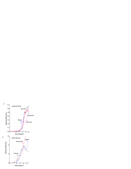
In Fig. 10 we compare our results with the experimental data of Wilcoxon et al. for Si NCs wilcoxon99 and Ge NCs. wilcoxon01 There is a good overall agreement in both cases especially with LFE, however, for the case of Si NCs this is much more satisfactory. The major discrepancies can be attributed to excitonic effects that are not included in our work. In the case of Si NCs (Fig. 10(a)), we also display the tight binding result of Trani et al. which also includes LFE. trani07
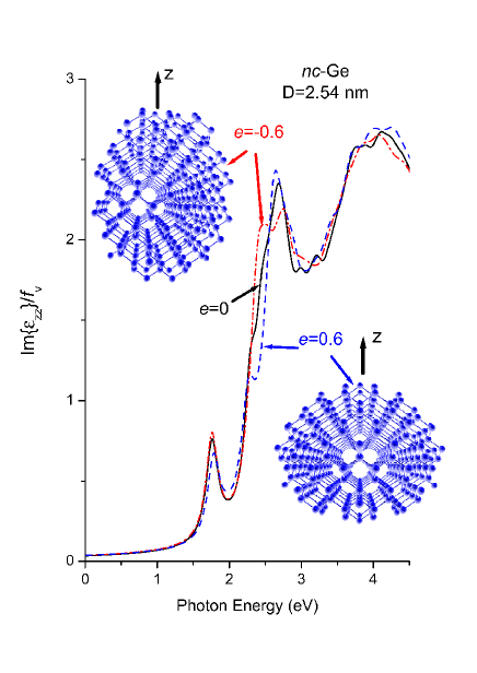
An issue of practical concern is the effect of deviation from the spherical shape of the NCs depending on the growth conditions. At this point we would like to investigate the effect of shape anisotropy on the interband absorption. Starting from a spherical 2.54 nm diameter Ge NC, we form prolate and oblate ellipsoidal NCs with ellipticities and +0.6, respectively. All three NCs contain the same number of 384 core atoms; the atomic arrangement of the ellipsoidal NCs are shown in the inset of Fig. 11. In the same figure we compare the components of the imaginary part of the dielectric tensor for three different ellipticities. It is observed that the effect on the interband absorption is not significant; the difference is even less for the Si NCs (not shown).
IV.4 Intraband absorption
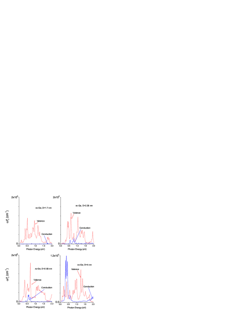
Unlike the interband case, for the intraband absorption we need to introduce electrons to the conduction states or holes to the valence states by an injection mechanism. We assume that after injection these carriers relax to their respective band edges and attain a thermal distribution. Therefore, we perform a Boltzmann averaging at room temperature (300 K) over the initial states around LUMO (HOMO) for electrons (holes). The absorption coefficients to be presented are for unity volume filling factors and for one carrier per NC; they can easily be scaled to a different average number of injected carriers and volume filling factors. In Fig. 12 the Si NCs of different diameters are compared. The intraband absorption is observed to be enhanced as the NC size grows up to about 3 nm followed by a drastic fall for larger sizes. For both holes and electrons very large number of absorption peaks are observed from 0.5 eV to 2 eV. Recently, de Sousa et al. have also considered the intraband absorption in Si NCs using the effective mass approximation and taking into account the multi-valley anisotropic band structure of Si.desousa However, their absorption spectra lacks much of the features seen in Fig. 12. Turning to Ge NCs, shown in Fig. 13 the intravalence band absorption profile is very similar to that of Si NCs, however in this case the intraconduction band absorption is much weaker.
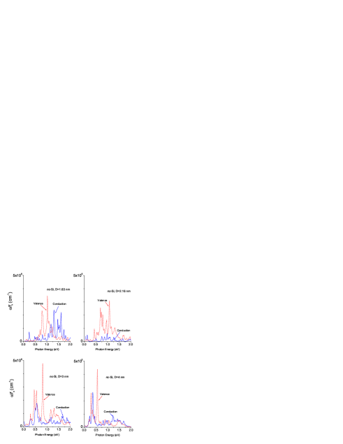
Mimura et al. have measured the optical absorption in heavily phosphorus doped Si NCs of a diameter of 4.7 nm. mimura This provides us an opportunity to compare our results on the intraconduction band absorption in Si NCs. There is a good order-of-magnitude agreement. However, in contrast to our spectra in Fig. 12 which contains well-resolved peaks, they have registered a smooth spectrum which has been attributed by the authors to the smearing out due to size and shape distribution within their NC ensemble. mimura
IV.5 Excited-state absorption
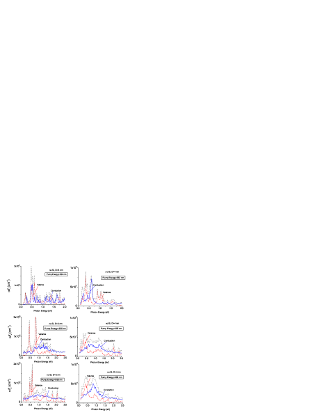
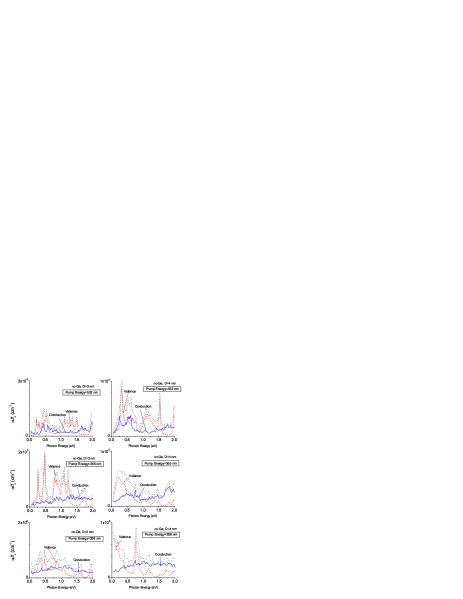
Finally, we consider another intraband absorption process where the system is under a continuous interband optical pumping that creates electrons and holes with excess energy. We consider three different excitation wavelengths: 532 nm, 355 nm and 266 nm which respectively correspond to the second-, third- and fourth-harmonic of the Nd-YAG laser at 1064 nm. The initial states of the carriers after optical pumping are chosen to be at the pair of states with the maximum oscillator strength bulutay07 among interband transitions under the chosen excitation. The determined energies of these states are tabulated in Table II where it can be observed that in general the excess energy is unevenly partitioned, mainly in favor of the conduction states. Once again a Boltzmann averaging is used to get the contribution of states within the thermal energy neighborhood.
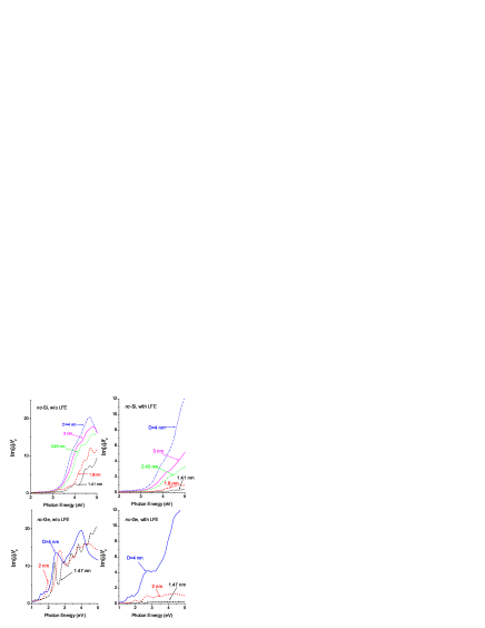
Considering 3 nm and 4 nm diameters, the results are shown in Figs. 14 and 15 for Si and Ge NCs, respectively. Note that the 532 nm excitation results are qualitatively similar to those in intraband absorption, cf. Figs. 12 and 13. This is expected on the grounds of small excess energy for this case. Some general trends can be extracted from these results. First of all, the conduction band absorption is in general smooth over a wide energy range. On the other hand the valence band absorption contains pronounced absorption at several narrow energy windows mainly below 1 eV and they get much weaker than the conduction band absorption in the remaining energies. As the excitation energy increases the absorption coefficient per excited carrier in general decreases. In connection to silicon photonics, we should point out that the excited-state absorption is substantial including the important 1.55 m fiber optics communication wavelength. These results provide a more comprehensive picture than the reported experimental measurements elliman ; forcales ; trojanek which are usually obtained at a single energy of the probe beam. Finally, it needs to be mentioned that for both intraband and excited-state absorptions displayed in Figs. 12 to 15, the high energy parts will be masked by the interband transition whenever it becomes energetically possible.
| nc-Si | nc-Ge | |||||
|---|---|---|---|---|---|---|
| Pump | nm | nm | nm | nm | ||
| 2.33 | 0.197, 0.021 | 0.021, 0.551 | 0.103, 0.643 | 0.211, 0.663 | ||
| 3.50 | 0.000, 1.432 | 0.316, 1.440 | 0.400, 1.508 | 1.141, 0.892 | ||
| 4.66 | 0.188, 2.414 | 0.713, 2.218 | 0.511, 2.551 | 1.360, 1.853 |
V Conclusions
The subject of Si and Ge NCs has become an established research field. A fundamental process such the direct photon absorption deserves further investigation from a number of perspectives. In this theoretical study, we consider the interband, intraband and excited-state absorption in embedded Si and Ge NCs of various sizes. For this purpose, we developed an atomistic pseudopotential electronic structure tool, the results of which agree very well with the published data. It is further observed that the HOMO for both Si and Ge NCs and the LUMO for Si NCs display oscillations with respect to size among different representations of the point group to which these spherical NCs belong. Our detailed investigation of the interband absorption reveals the importance of surface polarization effects that significantly reduce the absorption when included. This reduction is found to increase with decreasing NC size or with increasing permittivity mismatch between the NC core and the host matrix. These findings should be taken into account for applications where the absorption is desired to be either enhanced or reduced. For both NC types the deviation from sphericity shows no pronounced effect on the interband absorption. Next, the intraband process is considered which has potential applications on mid- and near-infrared photodetection. The intravalence band absorption is stronger compared to intraconduction band especially below 1 eV. Finally, we demonstrate that optical pumping introduces a new degrees of freedom to intraband absorption. This is studied under the title of excited-state absorption. Our major finding is that the excited-state absorption is substantial including the important 1.55 m fiber optics communication wavelength. Within the context of achieving gain and lasing in these NCs, excited-state absorption is a parasitic process, however, it can acquire a positive role in a different application.
Acknowledgements.
The author is grateful to Aykutlu Dâna for his suggestion of the intersubband absorption and its photodetector applications. This work has been supported by the European FP6 Project SEMINANO with the contract number NMP4 CT2004 505285 and by the Turkish Scientific and Technical Council TÜBİTAK with the project number 106T048. The computational resources are supplied in part by TÜBİTAK through TR-Grid e-Infrastructure Project.| (Å) | |||||||
|---|---|---|---|---|---|---|---|
| Si | 5.43 | 1.5708 | 2.2278 | 0.606 | -1.972 | 5.0 | 0.3 |
| Matrix-Si | 5.43 | 1.5708 | 2.5 | 0.135 | -13.2 | 6.0 | 0.3 |
| Ge | 5.65 | 0.7158 | 2.3592 | 0.74 | -0.38 | 5.0 | 0.3 |
| Matrix-Ge | 5.65 | 0.4101 | 2.7 | 0.07 | -2.2 | 5.0 | 0.3 |
Appendix: Some technical details on the LCBB implementation
In this section we first provide the details on the pseudopotential form factors of the bulk Si, Ge and their associated wide band-gap matrices to substitute for SiO2. We use the local empirical pseudopotentials for Si and Ge developed by Friedel, Hybertsen and Schlüter. friedel They use the following functional form for the pseudopotential form factor at a general wave number :
Using the parameters supplied in Table III, the pseudopotential form factors come out in Rydbergs and the wave number in the above equation should be taken in atomic units (1/Bohr radius). Another important technical remark is about the EPM cut off energies. We observed that even though the EPM band energies (i.e., eigenvalues) converge reasonably well with cut off energies as low as 5-10 Ry, the corresponding Bloch functions (i.e., eigenvectors) require substantially higher values to converge. bulutay06 The results in this study are obtained using 14 and 16 Ry for Si, Ge, respectively.
Finally, some comments on the LCBB basis set construction is in order. We only employ the bulk bands of the core material. The bulk band indices are chosen from the four valence bands an the lowest three to four conduction bands; usually these are not used in conjunction but separately for the NC valence and conduction states, respectively. The basis set is formed from a sampling over a three-dimensional rectangular grid in the reciprocal space centered around the -point. Its extend is determined by the full coverage of the significant band extrema, such as conduction band minima of Si at the six equivalent 0.85 X points. The final LCBB basis set typically contains some ten thousand members.
References
- (1) S. Ossicini, L. Pavesi, and F. Priolo, Light Emitting Silicon for Microphotonics, Springer-Verlag, Berlin, (2004).
- (2) L. Pavesi, L. Dal Negro, C. Mazzoleni, G. Franzó, and F. Priolo, Nature 408, 440 (2000).
- (3) R. J. Walters, G. I. Bourianoff, and H. A. Atwater, Nat. Mater. 4, 143 (2005).
- (4) H. Rong, A. Liu, R. Jones, O. Cohen, D. Hak, A. Fang, and M. Paniccia, Nature (London) 433, 292 (2005); H. Rong, R. Jones, A. Liu, O. Cohen, D. Hak, A. Fang, and M. Paniccia, Nature (London) 433, 725 (2005).
- (5) M. V. Wolkin, J. Jorne, P. M. Fauchet, G. Allan, and C. Delerue, Phys. Rev. Lett. 82, 197 (1999).
- (6) Z. Zhou, L. Brus, and R. Friesner, Nano Lett. 3, 163 (2003).
- (7) M. Luppi and S. Ossicini, Phys. Rev. B 71, 035340 (2005).
- (8) I. Sagnes, H. Halimaoui, G. Vincent, and P. A. Badoz, Appl. Phys. Lett. 62, 1155 (1993).
- (9) M. Green, Third Generation Photovoltaics, Springer-Verlag, Berlin, (2006).
- (10) S. Furukawa, and T. Miyasato, Phys. Rev. B 38, 5726 (1988).
- (11) Y. Kanemitsu, H. Uto, Y. Masimoto, and Y. Maeda, Appl. Phys. Lett. 61, 2187 (1992).
- (12) S. Takeoda, M. Fujii, S. Hayashi, and K. Yamamoto, Phys. Rev. B 58, 7921 (1998).
- (13) J. P. Wilcoxon, G. A. Samara, and P. N. Provencio, Phys. Rev. B 60, 2704 (1999).
- (14) D. Kovalev, J. Diener, H. Heckler, G. Polisski, N. Künzner, and F. Koch, Phys. Rev. B 61, 4485 (2000).
- (15) J. P. Wilcoxon, P. P. Provencio, and G. A. Samara, Phys. Rev. B 64, 035417 (2001).
- (16) I. Vasiliev, S. Öğüt, and J. R. Chelikowsky, Phys. Rev. Lett. 86, 1813 (2001).
- (17) H.-Ch. Weissker, J. Furthmüller and F. Bechstedt, Phys. Rev. B 65, 155327 (2002).
- (18) H.-Ch. Weissker, J. Furthmüller and F. Bechstedt, Phys. Rev. B 65, 155328 (2002).
- (19) H.-Ch. Weissker, J. Furthmüller and F. Bechstedt, Phys. Rev. B 67, 245304 (2003).
- (20) L. E. Ramos, H.-Ch. Weissker, J. Furthmüller and F. Bechstedt, Phys. Status Solidi B 242, 3053 (2005).
- (21) D. Melnikov and J. R. Chelikowsky, Solid State Commun. 127, 361 (2003); D. Melnikov and J. R. Chelikowsky, Phys. Rev. B 69, 113305 (2004).
- (22) A. Tsolakidis and R. M. Martin, Phys. Rev. B 71, 125319 (2005).
- (23) F. Trani, G. Cantele, D. Ninno, and G. Iadonisi, Phys. Rev. B 72, 075423 (2005).
- (24) Y. -Y. Lin and J. Singh, J. Appl. Phys. 96, 1059 (2004).
- (25) V. Ryzhii, I. Khmyrova, V. Mitin, M. Stroscio, and M. Willander, Appl. Phys. Lett. 78, 3523 (2001).
- (26) A. V. Malko, A. A. Mikhailovsky, M. A. Petruska, J. A. Hollingsworth, and V. I. Klimov, J. Phys. Chem. B 108, 5250 (2004).
- (27) R. G. Elliman, M. J. Lederer, N. Smith, and B. Luther-Davies, Nuc. Instrum. Methods Phys. Res., Sect. B 206, 427 (2003).
- (28) F. Trojánek, K. Neudert, M. Bittner, and P. Malý, Phys. Rev. B 72, 075365 (2005).
- (29) M. Forcales, N. J. Smith, and R. G. Elliman, J. Appl. Phys. B 100, 014902 (2006).
- (30) A. Zunger, Phys. Status Solidi A 190, 467 (2002).
- (31) R. M. Martin, Electronic Structure, Cambridge University Press, Cambridge (2004).
- (32) S. Öğüt, J. R. Chelikowsky, S. G. Louie, Phys. Rev. Lett. 79, 1770 (1997).
- (33) C. Delerue and M. Lannoo, Nanostructures: Theory and Modelling, Springer-Verlag, Berlin, (2004).
- (34) S. Y. Ren, Phys. Rev. B 55, 4665 (1997); S. Y. Ren, Solid State Comm. 102, 479 (1997).
- (35) Y. M. Niquet, G. Allan, C. Delerue, and M. Lannoo, Appl. Phys. Lett. 77, 1182 (2000).
- (36) L. -W. Wang and A. Zunger, J. Chem. Phys. 100, 2394 (1994).
- (37) L. -W. Wang, A. Franceschetti and A. Zunger, Phys. Rev. Lett. 78, 2819 (1997).
- (38) L. -W. Wang and A. Zunger, Phys. Rev. B 59, 15806 (1999).
- (39) D. Ninno, K. B. Wong, M. A. Gell and M. Jaros, Phys. Rev. B 32, 2700 (1985).
- (40) D. Ninno, M. A. Gell and M. Jaros, J. Phys. C: Solid State Phys. 19, 3845 (1986).
- (41) S. Botti and L. C. Andreani, Phys. Rev. B 63, 235313 (2001).
- (42) S. Botti, N. Vast, L. Reining, V. Olevano and L. C. Andreani, Phys. Rev. B 70, 045301 (2004)
- (43) F. Chirico, A. Di Carlo and P. Lugli, Phys. Rev. B 70, 045314 (2001).
- (44) C. Bulutay, Physica E 38, 112 (2007).
- (45) F. Iacona, G. Franzó, C. Spinella, J. Appl. Phys. 87, 1295 (2000).
- (46) An intermediate value between 0 and 1 can be used for the alloys or modeling the interface region. However, in this work we set them to either 1 or 0.
- (47) P. Friedel, M. S. Hybertsen, and M. Schlüter, Phys. Rev. B 39, 7974 (1989).
- (48) J. R. Chelikowsky, Solid State Commun. 22, 351 (1977).
- (49) J. D. Jackson, Classical Electrodynamics, 2nd edition, Wiley, New York (1975).
- (50) F. Trani, D. Ninno, and G. Iadonisi, Phys. Rev. B 75, 033312 (2007).
- (51) G. D. Mahan, Phys. Rev. B 74, 033407 (2006).
- (52) B. Delley and E. F. Steigmeier, Phys. Rev. B 47, 1397 (1993).
- (53) F. A. Reboredo and A. Zunger, Phys. Rev. B 63, 235314 (2001).
- (54) G. Onida, L. Reining, and A. Rubio, Rev. Mod. Phys. 74, 601 (2002).
- (55) H. Ehrenreich and M. H. Cohen, Phys. Rev. 115, 786 (1959).
- (56) M. S. Hybertsen, Phys. Rev. Lett. 72, 514 (1994).
- (57) L. -W. Wang and A. Zunger, J. Phys. Chem. 98, 2158 (1994).
- (58) F. A. Reboredo, A. Franceschetti, and A. Zunger, Phys. Rev. B 61, 13073 (2000).
- (59) C. Delerue, M. Lannoo, and G. Allan, Phys. Rev. Lett. 84, 2457 (2000).
- (60) C. S. Garoufalis, A. D. Zdetsis, and S. Grimme, Phys. Rev. Lett. 87, 276402 (2001).
- (61) J. S. de Sousa, J.-P. Leburton, V. N. Freire, and E. F. da Silva Jr., Appl. Phys. Lett. 87, 031913 (2005).
- (62) A. Mimura, M. Fujii, S. Hayashi, D. Kovalev, and F. Koch, Phys. Rev. B 62, 12625 (2000).
- (63) C. Bulutay, Turk. J. Phys. 30, 287 (2006).