Anisotropic low-temperature piezoresistance in (311)A GaAs two-dimensional holes
Abstract
We report low-temperature resistance measurements in a modulation-doped, (311)A GaAs two-dimensional hole system as a function of applied in-plane strain. The data reveal a strong but anisotropic piezoresistance whose magnitude depends on the density as well as the direction along which the resistance is measured. At a density of cm-2 and for a strain of about applied along [01], e.g., the resistance measured along this direction changes by nearly a factor of two while the resistance change in the [33] direction is less than 10% and has the opposite sign. Our accurate energy band calculations indicate a pronounced and anisotropic deformation of the heavy-hole dispersion with strain, qualitatively consistent with the experimental data. The extremely anisotropic magnitude of the piezoresistance, however, lacks a quantitative explanation.
The piezoresistance effect – the change of a device’s electrical resistance as a function of applied stress – is of great technological importance as it is utilized in making force, displacement and pressure sensors Marian92 . It has also been used recently in measuring sub-nanometer displacements of tips in atomic force microscopes TortoneseAPL93 ; HarleyAPL99 , and proposed data storage devices based on piezoresistive readback ChuiAPL96 .
Strain affects the resistance of a solid in two ways. It changes the physical dimensions of the resistor and can also modify its energy band structure. In metals, it is the former effect that is dominant and the the gauge factor, defined as the fractional change in resistance divided by the solid’s fractional change in length, is dictated by the Poisson’s ratio which is typically around 2. On the other hand, for certain semiconductors the modification of the band structure is a more prominent factor affecting the piezoresistance. In multi-valley semiconductor systems, for example, strain changes the relative population of the valleys. If the valleys have anisotropic effective masses, the charge transfer induces a large resistance change in certain crystallographic directions Smith54 . Gauge factors of 1500 have been reported for n-type Si inversion layers DordaSSC72 and 10,000 in AlAs two-dimensional (2D) electron systems at low temperatures ShkolnikovAPL04 .
In this Letter, we report a large, density (p) dependent piezoresistance effect in a (311)A GaAs 2D hole system (2DHS). We utilize a simple but powerful technique to apply quantitatively measurable in-plane strain in-situ ShayeganAPL03 and measure resistance parallel and perpendicular to the applied strain. We deduce a gauge factor of 3600 at cm-2 and K. The data can be qualitatively understood by the change in the heavy-hole valence band shape with applied strain. But a quantitative explanation of the observed piezoresistance magnitude and particularly its extreme anisotropy, is lacking.
Our sample is grown on a (311)A GaAs substrate by molecular beam epitaxy and contains a modulation-doped 2DHS confined to a GaAs/AlGaAs heterostructure. The Al0.35Ga0.65As/GaAs interface is separated from a 17 nm-thick Si-doped Al0.35Ga0.65As layer (Si concentration of cm-3) by a 30 nm Al0.35Ga0.65As spacer layer. We fabricated L-shaped Hall bar samples via photo-lithography and used In:Zn alloyed at 440∘C for the ohmic contacts. Metal gates were deposited on the sample’s front (10nm Ti; 30nm Au) and back (100nm Ti; 30nm Au) to control the 2D hole density. Magneto-resistance data taken at cm-2 and K yield mobilities of cm2/Vs and cm2/Vs in the [] and [] directions respectively. This mobility anisotropy in the (311)A growth direction stems from the quasi-periodic ridges along the direction WassermeierPRB95 ; HeremansJAL94 .
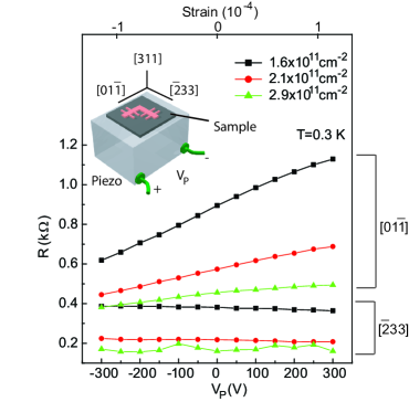
We apply tunable strain to the sample (thinned to ) by gluing it on one side of a commercial multilayer piezoelectric (piezo) actuator with the sample’s [] crystal direction aligned with the poling direction of the piezo (Fig. 1 inset) ShayeganAPL03 . When bias is applied to the piezo, it expands (shrinks) along the [] for () and shrinks (expands) along the [] direction. We have confirmed that this deformation is fully transmitted to the sample, and using metal strain gauges glued to the opposite side of the piezo, have measured its magnitude ShayeganAPL03 ; GunawanPRL06 . Based on our calibrations of similar piezo actuators, we estimate a strain of V-1 along the poling direction. In the perpendicular direction, the strain is approximately times the strain in the poling direction ShayeganAPL03 ; notepiezo . In this paper we specify strain values along the poling direction; we can achieve a strain range of about by applying V to the piezo notecooldown . Finally, the back-gate on the sample is kept at a constant voltage (0 V) throughout the measurements to shield the 2DHS from the electric field of the piezo actuator.
Figure 1 summarizes our measured piezoresistance. Three trends in the data are clear. First, the change in resistance (R) with strain is density dependent and is larger for lower densities. Second, the piezoresistance is more prominent along the [01] direction. Indeed, at cm-2, R along this direction changes by a remarkable factor of two for an applied strain of only . Third, in the entire strain range we have studied, R along [01] is always larger than in the [33] direction.


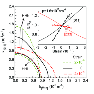
In order to understand the data of Fig. 1, we performed self-consistent calculations of the Fermi contours of the 2D holes residing in the heavy-hole (HH) valence band as a function of strain. Note that in this system the spin degeneracy of the HH band is lifted due to the presence of strong spin-orbit coupling Winkler03 . The spin subbands are termed heavy HH (HHh) and light HH (HHl), reflecting the magnitude of their effective masses. We used the Kane Hamiltonian, augmented by the strain Hamiltonian of Bir and Pikus Winkler03 ; Bir74 , to take into account the spin-orbit coupling of the system as well as the strain-induced contributions. We adapted this model to the (311) orientation of our sample by a suitable coordinate transformation. We note that these energy band calculations are quite accurate and have quantitatively explained the spin-orbit induced spin-splitting and its dependence on density, electric field and strain in 2DHSs LuPRL98 ; PapadakisPHE01 ; HabibPRB07 .
The results of the energy band calculations for our sample parameters are shown in Fig. 2. Since all the densities show similar trend, we only discuss results for cm-2. Figure 2 shows that the anisotropy of the HHh band is strongly enhanced with the application of strain. This results in the anisotropy of the HHh effective mass as well. Qualitatively, a larger Fermi wavevector in a particular direction typically implies a larger mass in the same direction. Hence, applying tensile strain along the [01] direction leads to a larger mass along [01] and a smaller mass along [33]. This change in effective mass qualitatively explains the change in resistance in the two directions.
To make a direct comparison with the experimental data, we calculated the resistance for our sample parameters taking the strain dependence of the anisotropy into account. We assume a constant and isotropic relaxation time () and sum over spin subbands, , with energy dispersion . We evaluate the velocity, at and to obtain the conductance () Chambers90 ,
| (1) |
Since it is difficult to estimate the value of , we normalize the calculated resistance to its value at zero strain and compare the calculations to the data of Fig. 1. For the comparison shown in the inset of Fig. 2, the experimental resistance was also normalized to the resistance at zero applied piezo bias, . As the figure shows, the calculations certainly match the qualitative trend seen in the data. It should be noted that the calculations are based on the particular sample structure and density but contain no fitting parameters.

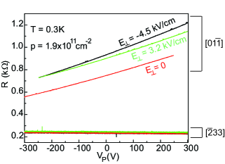
A puzzling aspect of Fig. 2 (inset) data is that in the [01] direction, the experimental change in resistance is typically larger than predicted by the calculations. The [33] direction, on the other hand, exhibits a much smaller change in the measured resistance than in the calculations. It is tempting to relate this mismatch to how the quasi-periodic corrugations WassermeierPRB95 parallel to [33] might affect the directional dependence of with strain. However, our piezoresistance measurements on a 20 nm square quantum well sample, as a function of perpendicular electric field () at a constant density, indicate otherwise [Fig. 3]. The square well sample is glued to the piezo with the poling direction in the [] crystal direction. is tuned while keeping the density constant with the help of front () and back () gate biases noteQW . At , the confining potential of the square well and the carrier wavefunction are symmetric. For , the potential becomes asymmetric, resulting in the carriers being ‘pushed’ closer to the interface. Hence the resistance increases with the increase in the magnitude of because of interface roughness, as shown in Fig. 3 at a particular piezo bias. If the direction dependent mismatch of the piezoresistance were related to the corrugations along [33], we would expect a larger piezoresistance mismatch with an increase in the magnitude of . On the contrary, Fig. 3 shows that the piezoresistance is nearly independent of notecont .
Moreover, a similar mismatch was also observed in (100) GaAs 2DHSs KolokolovPRB99 , where the change in resistance was reported to be larger than the calculated values in the [011] direction, while along [01] the measured change was much smaller than predicted by the calculations. The mobility anisotropy in (100) GaAs 2D holes at zero strain is only about 1.2-1.3 between the two perpendicular ([01] and [011]) in-plane directions. This is much smaller than the (311)A samples where the mobility anisotropy is typically about 2 to 3 between the [01] and [33] directions. It is unlikely, therefore, that the corrugations in (311)A samples are responsible for the mismatch between the rate of change of resistance along the [01] and [33] directions. We emphasize that this mismatch is independent of the poling direction of the applied strain: Our measurements on a different heterostructure sample from the same wafer as the one used in Fig. 1 but glued on a piezo actuator with the poling direction along the [33] direction also exhibit a larger change in resistance in the [01] direction compared to [33].
In conclusion, we observe a large piezoresistance effect in (311)A GaAs 2DHSs. The data indicate a strong dependence on density, and on the in-plane direction along which the resistance is measured. The maximum strain gauge factor we measure (along [01] and for cm-2) is . This value is comparable to the ones reported, at liquid He temperatures, for p-type Si (110) inversion layers at cm-2 DordaCON72 and for GaAs 2DHS grown in the (100) direction at cm-2 KolokolovPRB99 .
We thank the ARO, DOE and NSF for support, and M. Grayson for stimulating discussions.
References
- (1) A. Belu-Marian, E. Candet, and A. Devenyi, Thin film resistive sensors (IOP Publishing, 1992), p. 113.
- (2) M. Tortonese, R. C. Barrett, and C. F. Quate, Appl. Phys. Lett. 62, 834 (1993).
- (3) J. A. Harley and T. W. Kenny, Appl. Phys. Lett. 75, 289 (1999).
- (4) B. W. Chui, T. D. Stowe, T. W. Kenny, H. J. Mamin, B. D. Terris, and D. Rugar, Appl. Phys. Lett. 69, 2767 (1996).
- (5) C. S. Smith, Phys. Rev. 94, 42 (1954).
- (6) G. Dorda, I. Eisele, and E. Preuss, Solid State Comm. 11, 1625 (1972a).
- (7) Y. P. Shkolnikov, K. Vakili, E. P. De Poortere, and M. Shayegan, Appl. Phys. Lett. 85, 3766 (2004).
- (8) M. Shayegan, K. Karrai, Y. P. Shkolnikov, K. Vakili, E. P. De Poortere, and S. Manus, Appl. Phys. Lett. 83, 5235 (2003).
- (9) M. Wassermeier, J. Sudijono, M. D. Johnson, K. T. Leung, B. G. Orr, L. Däweritz, and K. Ploog, Phys. Rev. B 51, 14721 (1995).
- (10) J. J. Heremans, M. B. Santos, K. Hirakawa, and M. Shayegan, J. of Appl. Phys. 76, 1980 (1994).
- (11) O. Gunawan, Y. P. Shkolnikov, K. Vakili, T. Gokmen, E. P. De Poortere, and M. Shayegan, Phys. Rev. Lett. 97, 186404 (2006).
- (12) The strain in the perpendicular direction is taken into account in our calculations described later in the paper.
- (13) In our experiments, we can determine the relative changes in values of strain accurately, but not the piezo-bias corresponding to zero-strain precisely. This is because, thanks to a mismatch between the thermal expansion coefficients of GaAs and the piezo-stack, at low temperatures the sample can be under finite strain even at . This residual strain is cooldown-dependent and we do not know its precise value for our data. Based on our experience with cooldowns of samples glued to similar piezo-stacks, we expect a residual strain up to about .
- (14) R. Winkler, Spin-Orbit Coupling Effects in Two-Dimensional Electron and Hole Systems (Springer, Berlin, 2003).
- (15) G. L. Bir and G. E. Pikus, Symmetry and strain-induced effects in semiconductors (Wiley, New York, 1974).
- (16) J. P. Lu, J. B. Yau, S. P. Shukla, M. Shayegan, L. Wissinger, U. Rössler, and R. Winkler, Phys. Rev. Lett. 81, 1282 (1998).
- (17) S. J. Papadakis, E. P. De Poortere, M. Shayegan, and R. Winkler, Physica E 9, 31 (2001).
- (18) B. Habib, J. Shabani, E. P. De Poortere, M. Shayegan, and R. Winkler, Phys. Rev. B 75, 153304 (2007).
- (19) R. Chambers, Electrons in Metals and Semiconductors (Chapman & Hall, London, 1990).
- (20) For details of the square quantum well sample structure and tuning the wavefunction symmetry see: S. J. Papadakis, E. P. De Poortere, M. Shayegan, and R. Winkler, Physica E 9, 31 (2001).
- (21) This independence of the piezoresistance on is corroborated by our calculations of the Fermi contours as a function of for our quantum well.
- (22) K. I. Kolokolov, A. M. Savin, S. D. Beneslavski, N. Y. Minina, and O. P. Hansen, Phys. Rev. B 59, 7537 (1999).
- (23) G. Dorda, I. Eisele, and E. Preuss, in Proceedings of the 11th Int. Conf. on Physics of Semicondcutors (Academic, New York, 1972b), pp. 1468–1473.