A microfabricated sensor for thin dielectric layers
Abstract
We describe a sensor for the measurement of thin dielectric layers capable of operation in a variety of environments. The sensor is obtained by microfabricating a capacitor with interleaved aluminum fingers, exposed to the dielectric to be measured. In particular, the device can measure thin layers of solid frozen from a liquid or gaseous medium. Sensitivity to single atomic layers is achievable in many configurations and, by utilizing fast, high sensitivity capacitance read out in a feedback system onto environmental parameters, coatings of few layers can be dynamically maintained. We discuss the design, read out and calibration of several versions of the device optimized in different ways. We specifically dwell on the case in which atomically thin solid xenon layers are grown and stabilized, in cryogenic conditions, from a liquid xenon bath.
keywords:
Capacitive sensor , thin filmsPACS:
: 07.07.Df, 68.43.-h1Now at Stanford Linear Accelerator Center, Menlo Park, CA 94025
1 Introduction
The ability to detect atomically thin layers of materials deposited onto a substrate is essential in many branches of science and technology. By far the most common method employs “microbalances” [2], piezoelectric quartz oscillators whose resonant frequency changes as the material deposited onto the crystal increases the mass associated with its surface atomic layer. Microbalances, however, can only produce high resolution measurements if they operate in a medium that does not substantially reduce their mechanical quality factor. In particular they are not suitable for operation in liquids that, because of viscosity, substantially damp the crystal oscillations.
The sensor development discussed here arises from the need to measure thin layers of solid xenon (SXe) grown on a probe that is immersed in liquid xenon (LXe) at 170 K and further cooled. In the context of the EXO neutrino-less double-beta () detector R&D program [3], the need arises to retrieve and identify single barium ions produced by the decays of 136Xe. In a possible design of the experiment, several tons of 136Xe in liquid phase would serve as the source of decay as well as the detection medium in a time projection chamber (“TPC” [4]). Candidate decays would be localized by the TPC and a mechanical extraction device would be inserted in the LXe, retrieve the Ba-ion and transport it into an ion trap. While single Ba-ion identification in a trap filled with buffer gases including Xe has already been achieved [5, 6], the device to transport single ions from LXe to the low pressure ion trap with high efficiency is still being developed. One technology under investigation consists of electrostatically attracting the Ba-ion onto a probe tip coated with SXe. Due to its large ionization potential, SXe isolates the chemically active ion from the substrate material and makes subsequent release possible, by sublimation of the coating in vacuum. The requirement that only a very small amount of Xe be released in the ion trap calls for the development of a SXe sensor capable of operation in LXe with sensitivity of a few atomic layers.
The sensor is based on a microfabricated capacitor composed of two arrays of interleaved metallic fingers on a dielectric substrate. The fingers are exposed to the environment to be measured so that their mutual capacitance depends on the dielectric constant of the environment, assumed to be dielectric. The possibility of making extremely sensitive capacitance measurements allows for detecting very small changes in . While only capacitance measurements are used in the rest of this work, the combined measurement of capacitance and loss factor as function of the frequency is a common way of characterizing bulk dielectrics [7] and could extend the range of application for devices of the type discussed here. Possible applications include the measurement of thin layer deposition in gaseous and liquid environments, the detection of certain chemical species in gas and liquids or the fast analysis of certain immiscible (multiphase) liquids (e.g. oil-water emulsions). The clean, rugged, simple and small design of the device is suitable for a variety of environments, from UHV to in-situ geological measurements.
2 Description and fabrication of the device
A magnified picture of a sensor is shown in Fig. 1 (a). The darker line represents the gap between the aluminum fingers. The overall circular configuration makes the sensor suitable for mounting at the end of a small-diameter ( 1-2 mm) probe and is otherwise irrelevant for the performance of the device. The test device shown in Fig. 1 (a) is not yet cut in the final circular shape. A 200 m-thick quartz wafer is used as substrate. Various structures with different Al-strip width , spacing , thickness and overall diameter are produced, resulting in capacitances up to 30 pF in vacuum. All devices discussed here are produced using optical lithography.
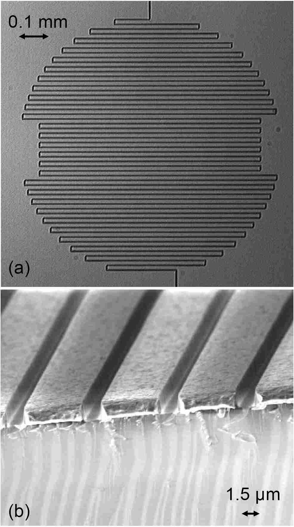
Different parameters are optimized as follows: the overall diameter has to be small for our application, so that the device can be mounted on the tip of a thin probe capable of being inserted in the LXe detector as well as into an ion trap. Devices were produced with from 0.94 to 1.9 mm. The spacing between the metallic fingers and their thickness are important to obtain good sensitivity for a particular range of thicknesses of frozen material. We chose m and m, so that the spaces to be filled by the medium under measurement have a roughly square cross section. The width of the aluminum strips was varied quite substantially in different devices as thin strips provide larger capacitance per unit area but may be more fragile (unlike most electronic devices, this sensor has to be exposed directly to different fluids). The devices discussed here have capacitances in vacuum in the range of 2 pF to 30 pF. The series resistance of the devices (due to the small cross section of the strips) is in all cases negligible with respect to the reactance at the frequencies (1 kHz to 1 MHz) used for the capacitive measurements.
Device fabrication begins with coating the top side of a quartz wafer with 2 m aluminum. The Al is then covered with 1.6 m Shipley 3612 positive photoresist that is then exposed to 350 nm light for 1.6 s through a vacuum contacted photolithography mask. After developing, the structure is etched into the Al layer using reactive ion plasma etching with optical endpoint detection in an Applied Materials P5000 etcher. The residual photoresist is removed using SVC PRX-127 resist stripper. The line spacing of m is close to the technical limit for using contact masks. A scanning electron microscope picture of the walls of the etched channels is shown in Fig. 1 (b). Wafers are covered with protective tape, diced in a square shape and directly used or later ground into a roughly circular shape. The yield of this rather crude process is 50%, sufficient for our purpose, although clean circular cutting could be achieved using standard techniques (e.g. bead blasting or laser cutting).
An overview of all sensors produced is given in Tab. 1. The capacitance values in this table are measured in air and hence are intended only for generic sensor characterization. The measurements for the table are obtained at a readout frequency of 10 kHz, but no significant change in capacitance is observed in the 100 Hz - 2 MHz frequency range explored. Taking edge effects into account, the capacitance scales with the geometrical dimensions as expected. It should be noted that we also produced sensors with nm and nm using electron-beam lithography and plasma etching of 300 nm thick aluminum. These structures were found to be too small to grow consistent frozen layers between strips and will not be discussed further.
3 Cryogenic setup and readout
The sensor can be configured in many different ways to detect thin layers of different dielectric materials of interest. While testing with water and other materials freezing near room temperature is rather straight forward, here we describe a more elaborate system that was developed to make tests at cryogenic conditions and, in particular, maintain stable SXe layers at a variety of pressures by cooling the sensor with liquid helium (LHe) to arbitrary temperatures as low as 20 K. The setup also allows to heat the sensor up to 650 K to sublimate the coating.
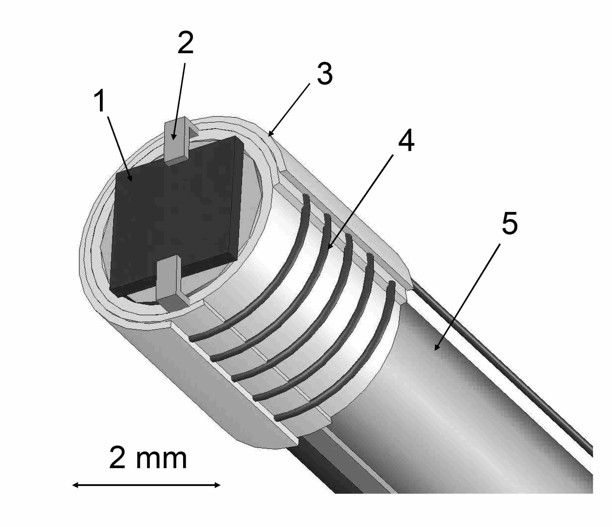
Most of the data presented in this paper was collected with this advanced setup or with simpler arrangements. The sensor is thermally and mechanically connected to a copper cold finger using VGE-7031 varnish or indium. Gold-plated readout leads are pressed against the sensor’s Al pads and a thin walled Vespel[8] polyimide tube section is forced around the leads to make the setup sturdy and strain relief the contacts. UHV-rated ultraminiature polyimide-insulated coaxial cables type ”SC” from Lakeshore[9] are run along the stem of the cryostat and bring the signals to room temperature. Figure 2 schematically shows one device mounted on the tip of the cold finger, together with a 0.05 mm tungsten heater wire.
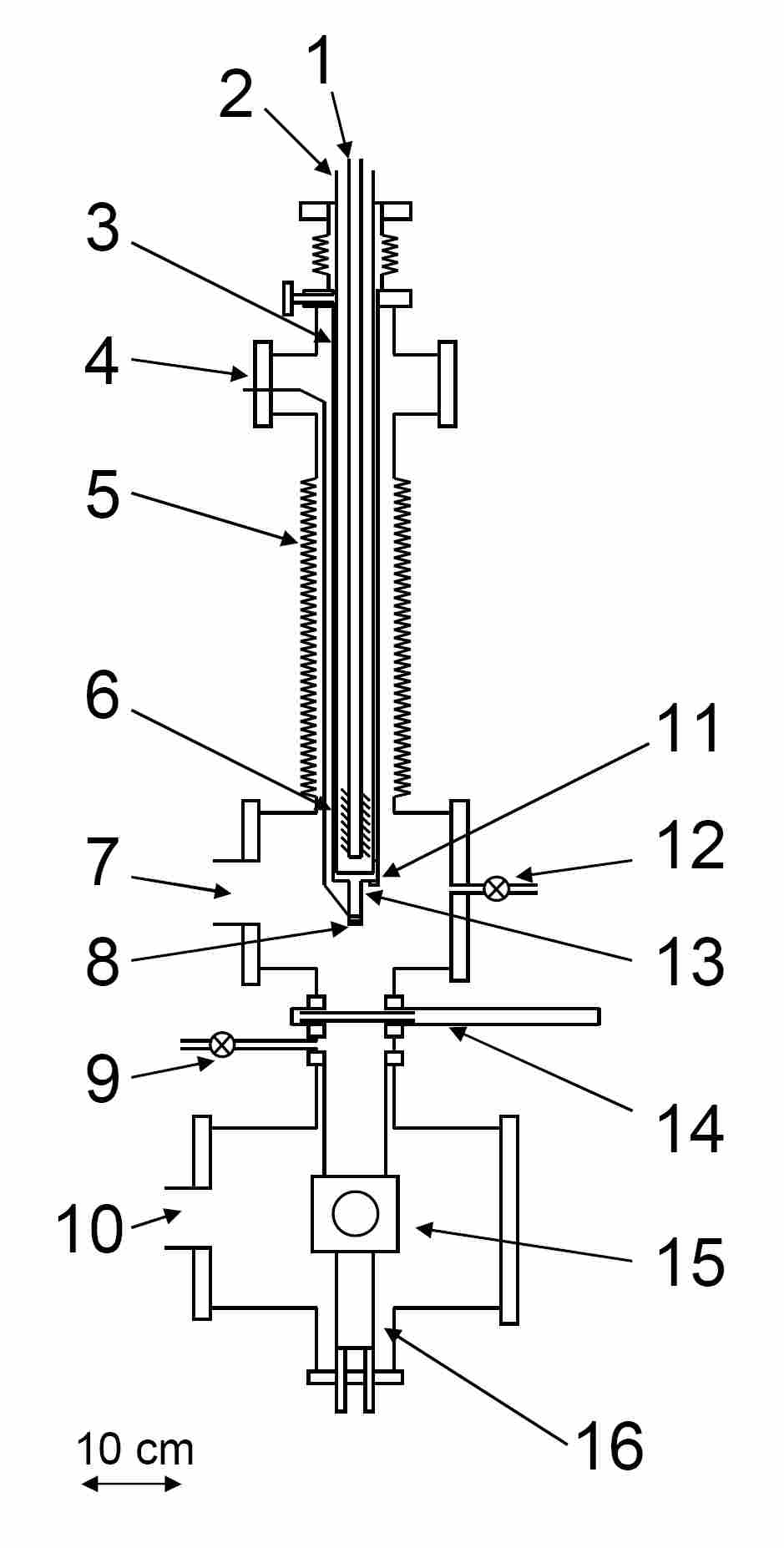
The cold finger is mounted in the setup schematically shown in Fig. 3. With reference to the figure, LHe is injected through the central vacuum insulated line from the top of the cryostat (1), it cools the cold finger (13) and sensor (8) through a copper heat exchanger (6) and is exhausted from the coaxial line (2). The entire LHe assembly is surrounded by a 9 mm diameter vacuum jacket (3). The tungsten heater wrapped around the cold finger has a maximum power of about 2.5 W and is used to fine tune the temperature of the tip and selectively evaporate frozen layers. The cooled probe can be translated vertically by 40 cm with a set of bellows (5) and a pneumatic actuator (not shown), so that it can be inserted into a small LXe cell (15) cooled by a second, larger cold finger (16) submerged in liquid nitrogen (LN2). With this setup, layers can be grown from gas or liquid phase from a variety of media. All temperatures and pressures are readout by a LabView[10] control system that operates valves, heaters and the vertical position of the probe, allowing for fully automated operation of the system. Because of the small dimensions of the probe assembly only two coaxial wires are used for the connection of the sensor to the vacuum feedthrough (item 4 in Fig. 3), while a four wire setup is used outside of the vacuum system. This arrangement, though not ideal, provides sufficiently low noise for the measurements. An Agilent E4980A capacitance bridge able to excite the capacitor at 800 kHz while reading out at 20 sampless is used for the more critical measurements shown below. This instrument, capable of resolving 0.1 fF at our sampling rate, is particularly useful when fast response is required in a PID loop to stabilize layer thicknesses. Alternative readouts schemes include an Andeen-Hagerling 2550A ultra-high precision capacitance bridge and a relatively inexpensive SRS 715 bridge. A home-built, custom tuned circuit mounted at the vacuum feedthrough was also used for some of the measurements. Conceivably, a similar circuit built on a chip and placed next to the sensor itself could provide the best noise performance for the system while simplifying the wiring. In all cases two very stable 5 nF high voltage mica capacitors are used to decouple the readout electronics from the sensor. In this way, the sensor can be DC-biased up to a few kV, as it is required to attract Ba-ions in EXO. The temperature response of the sensors in vacuum was tested over the entire 15 K - 650 K range. The behavior during cooldown from 310 K to 15 K is shown in Fig. 4.
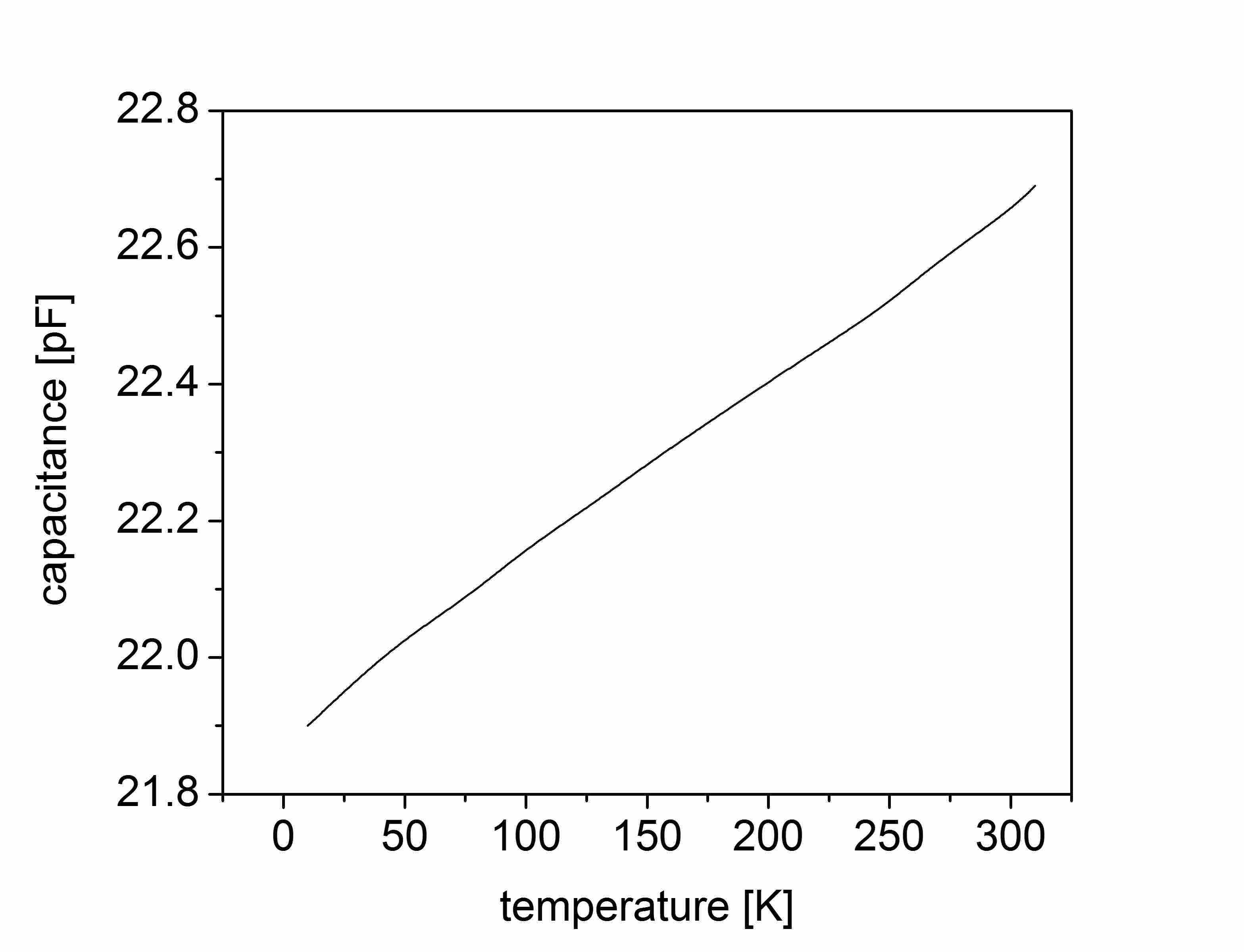
This is found to be well modeled by accounting for the thermal expansion of the Al strips and the quartz substrate. Overall the capacitance exhibits a small and positive temperature coefficient, as expected because the expansion coefficient of aluminum ( = 23.1 K-1) is substantially larger than that of quartz ( = 5.5 K-1). This measurement is not appreciably affected by condensation because of the low base pressure of mbar, and the fast cooldown time of 30 s from about 160 K to 20 K. A sensor calibration curve in vacuum is measured for every sensor type and used to correct all data presented below.
4 Sensor Performance
Once the offset capacitance of a particular sensor with its readout cables has been precisely established in the fluid phase (gas or liquid) of a dielectric material, its gain can be established by condensing a very thick layer ( 1000 nm) of the frozen phase, as determined by the saturation capacitance obtained in this way.
To verify that the saturation behavior is a proper normalization for the device at any thickness, a detailed calibration is performed for water and silicon oxide. These two calibratations involve very different systematic effects and their agreement with the finite element calculations demonstrates the accuracy of the devices. In the first case, water is frozen on a sensor by coupling the vacuum system to a small deionized water reservoir via a leak valve. The dielectric constant of water ice is 3.2 at high frequencies [11]. The measurement is performed by establishing equilibrium between the leak rate of vapor into the vacuum system and pumping through a throttled turbo molecular pump. By measuring the difference in equilibrium pressure with the cryostat at 300 K (4.110-5 mbar) and at 100 K (6.610-6 mbar), a deposition rate of 8.4atoms/(scm2) can be calculated. This corresponds to a thickness growth rate of 0.270.03 nm/s, assuming crystalline ice formation. Figure 5 shows the measured capacitance for H2O as a function of calculated layer thickness. In a second experiment, the response of the sensor was compared to a quartz crystal microbalance. For this test, uniform dielectric silicon oxide layers were repeatedly deposited on a wafer with sensors of types 6, 7 and 8 by means of low temperature vapor deposition in steps of about 200 nm. Capacitance was measured on different structures close to the center of the wafer and averaged. The dominant thickness uncertainty in this case originates from the wet-etch cleaning step before each further deposition step and is included in the error bars in the figure.
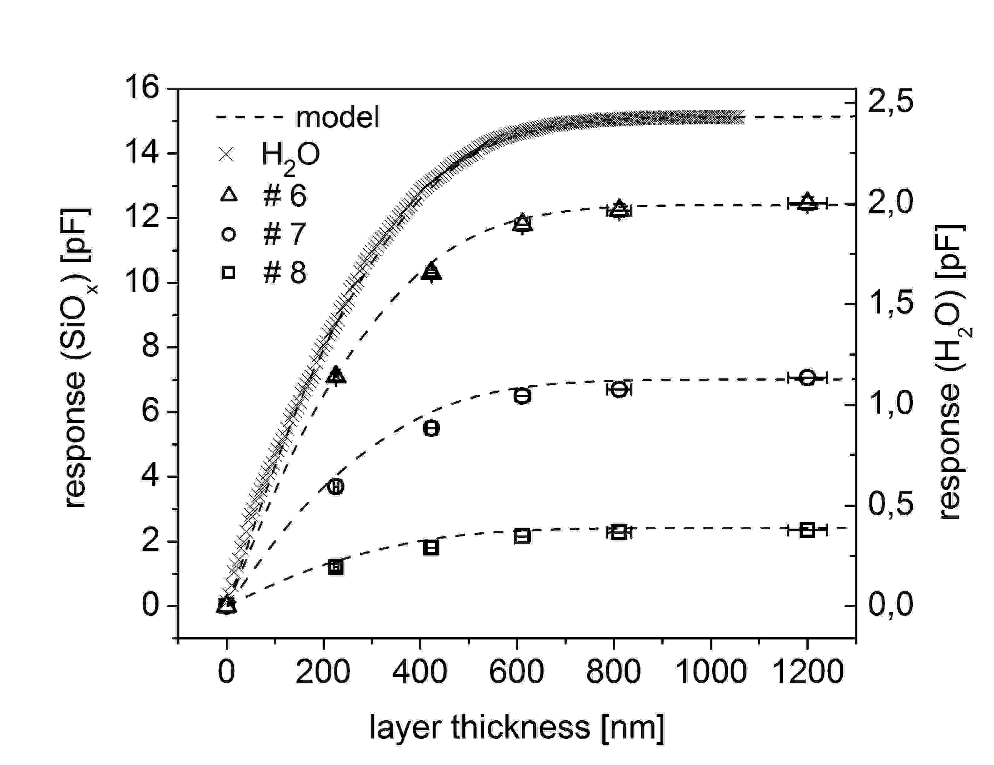
The dashed lines in Fig. 5 correspond to the result of a simulation of the response in each case using FEMLAB [12]. The simulation is based on the detailed geometry of the aluminum fingers and is carried out for different dielectric layer thicknesses, resulting in a very specific sensor response curve. This curve is then vertically stretched to fit the measured saturation value without changing its characteristic shape. The good agreement between data and simulation shows that the physics of the device is well understood, once the exact value of the dielectric constant is extracted from data.
The saturation capacitance () is also measured for several other materials in solid and liquid phase, as summarized in Tab. 2. Using the same FEMLAB simulation, the sensitivity of the sensor is then calculated for the first nm layer where the response is expected to be linear. This sensitvity parameter is also calculated from the saturation response of sensors fully submerged in liquids (although in practice, thin liquid layers are experimentally unattainable). The ratio between saturation capacitance and dielectric constant of the material is expected to be a property of the geometry of the sensor. This is verified, for two different sensor types, by the data shown in Tab. 2.
5 Accurate layer control with xenon
Several measurements were performed with the capacitive sensors to develop the ability to grow, stabilize and remove precisely controlled solid layers in different environments. The sublimation rate is described by the Hertz-Knudsen model [17], which approximates the net surface flux (in atoms cm-2 s-1) as
| (1) |
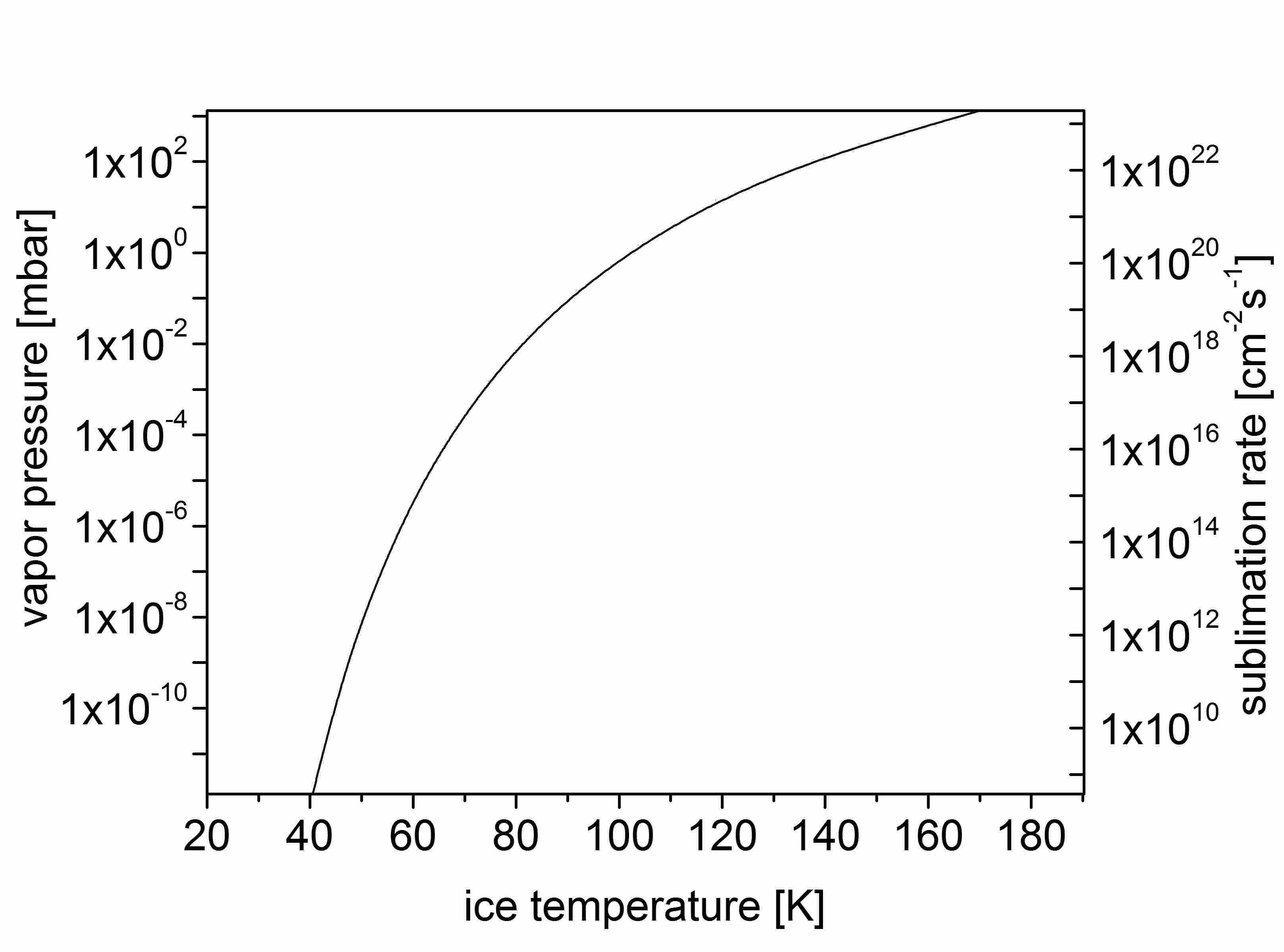
with the sticking coefficient (typically 0.1-1) the equilibrium vapor pressure at the temperature of the surface and the ambient pressure (for the case of vacuum ). The parameter is the mass of the atomic species sublimating and is Boltzmann’s constant. As an example, the values for for the case of Xe are computed using Ref. [18] and shown in Fig. 6. On the right axis the estimated sublimation rate in vacuum with = 1 is indicated.
In a first test, solid Xe layers are grown from the gas phase and kept stable for typical times of 100 s in vacuum. To condense a layer, the tip with the sensor is cooled below 30 K and a leak valve (item 12 in Fig. 3) is opened to set the partial pressure of Xe to mbar in the vacuum system. Controlled sublimation is obtained by increasing the probe tip temperature by gradually reducing the LHe flow through the cryostat. The data shown in Fig. 7 is collected with a sensor of type 5 (see Tab. 1).
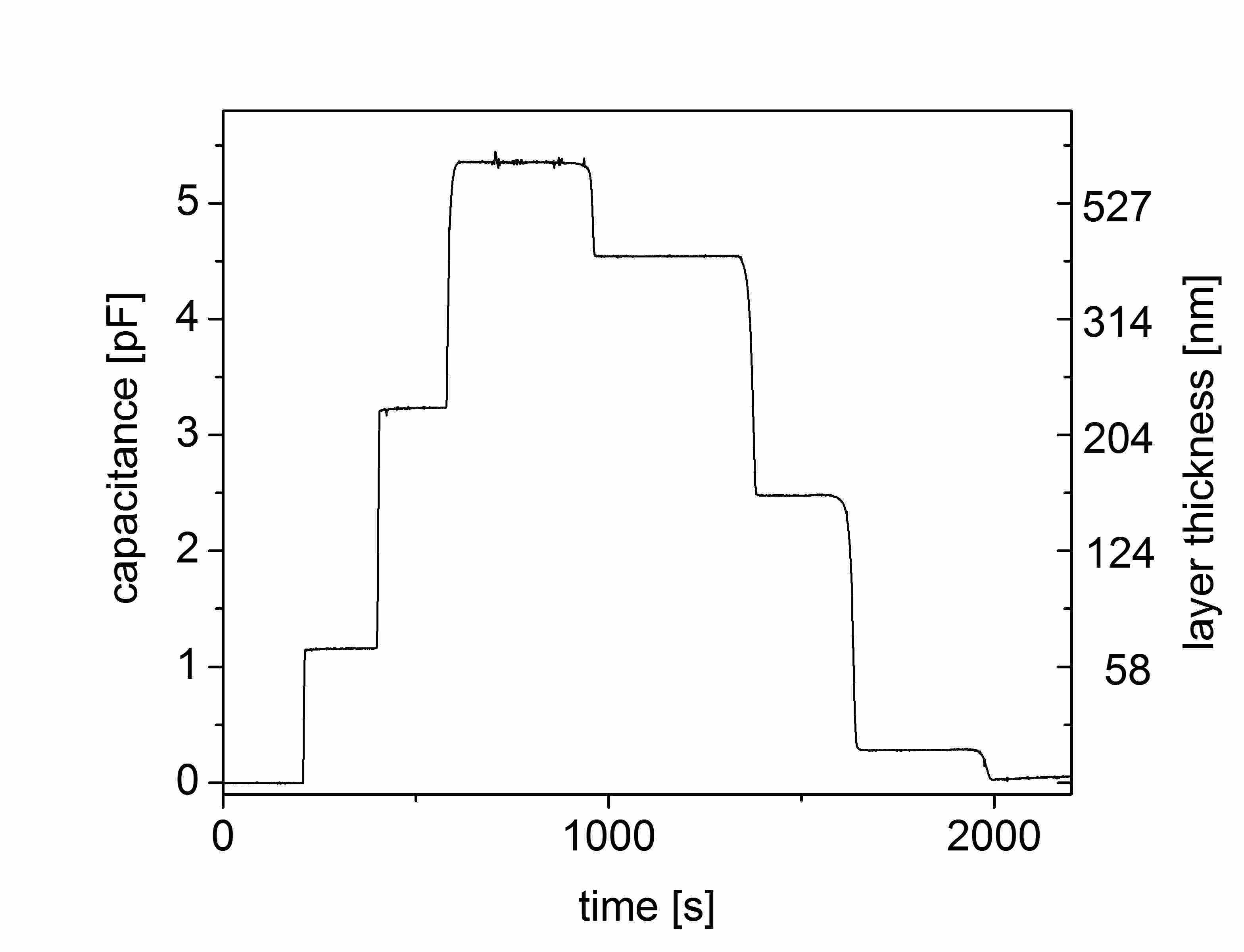
The thicknesses of the layers in the figure are, from left to right, 67.70.1 nm, 2240.2 nm, 750 nm (thicker than saturation), 403.10.1, 159.90.5 nm and 15.80.1 nm. No sublimation within the sensitivity of the device is observed in a 310-8 mbar vacuum at a tip temperature of 30 K. The errors on these measurements are dominated by the noise of the readout cables and the SRS 715 capacity bridge, which was used for this test and set to ”slow” readout (10 kHz excitation and 9 sample averaging at 4 samples/s using a two wire measurement).
A somewhat more challenging task consists of actively growing and stabilizing a solid Xe layer condensed from an infinite supply of Xe gas at 700 mbar and a temperature of 155 K. In this case the temperature of the probe has to be actively maintained in a feedback loop using the capacitance readout from the sensor. The LHe flow is kept constant while some heat is added to the tip by powering the tungsten wire (item 4 in Fig. 3) from a PID control loop realized within the LabView program. Stabilization is based directly on the layer thickness, which is calculated online from the capacitance of the sensor, correcting for the temperature coefficient, as explained. In this case, the capacitance is measured using the Agilent bridge with ”fast” readout setting (20 samples/s) and 4 sample averaging at 800 kHz excitation frequency. The PID loop has a cycle length of 50 ms. In Fig. 8 a series of PID-stabilized layers based on a sensor of type 9 is shown.
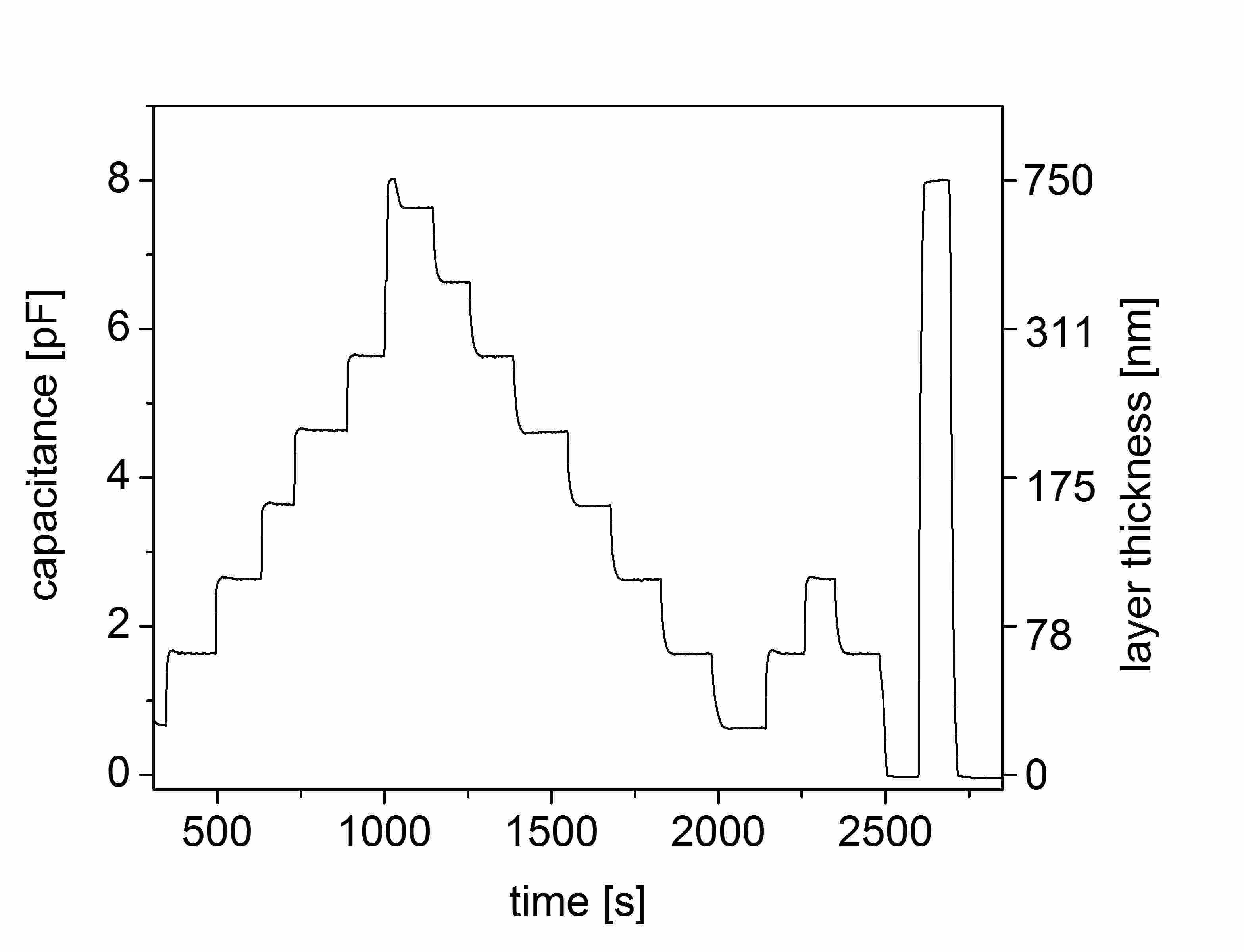
The sensor has a saturated capacitance for SXe at 155 K of 7.9790.003 pF. This corresponds to a response of 16.62 fF/nm for layers 100 nm (see Tab. 2). The layer thicknesses chosen for this test are 24.30.7 nm, 62.11.3 nm, 107.21.5 nm, 156.72.3 nm, 214.5 2.8 nm, 284.45.1 nm, 38310 nm and 567 40 nm, where the errors are the maximum deviation from the average value during the PID stabilization. The errors are dominated by the stability of the PID control loop. Again, layers stable for several minutes are clearly achieved. With the same setup the temperature of the cryostat was changed from 155 K to 10 K and the expected increase in the dielectric constant of 6.4% with the change in density of the solid [16] was indeed observed.
In order to freeze Xe from the liquid phase, the gate valve (item 14 in Fig. 3) below the probe tip is opened and the bellows (item 4 in Fig. 3) is compressed, so that the tip assembly with a sensor of type 10 reaches into a cold cell filled with liquid Xe (item 15 in Fig. 3). A customized LabView PID loop is used to control the current through the tungsten heater. Data were taken with the Agilent capacity bridge also using the ”fast” readout setting and only two samples averaging, which allows for a shorter PID cycle length of 20 ms. In order to keep conditions stable, the temperature of the liquid Xe cell is stabilized with a separate PID control loop to 163.000.03 K, which contains an unknown offset due to the position of the thermocouple on the outside of the LXe copper cell. The data for this case are shown in Fig. 9.
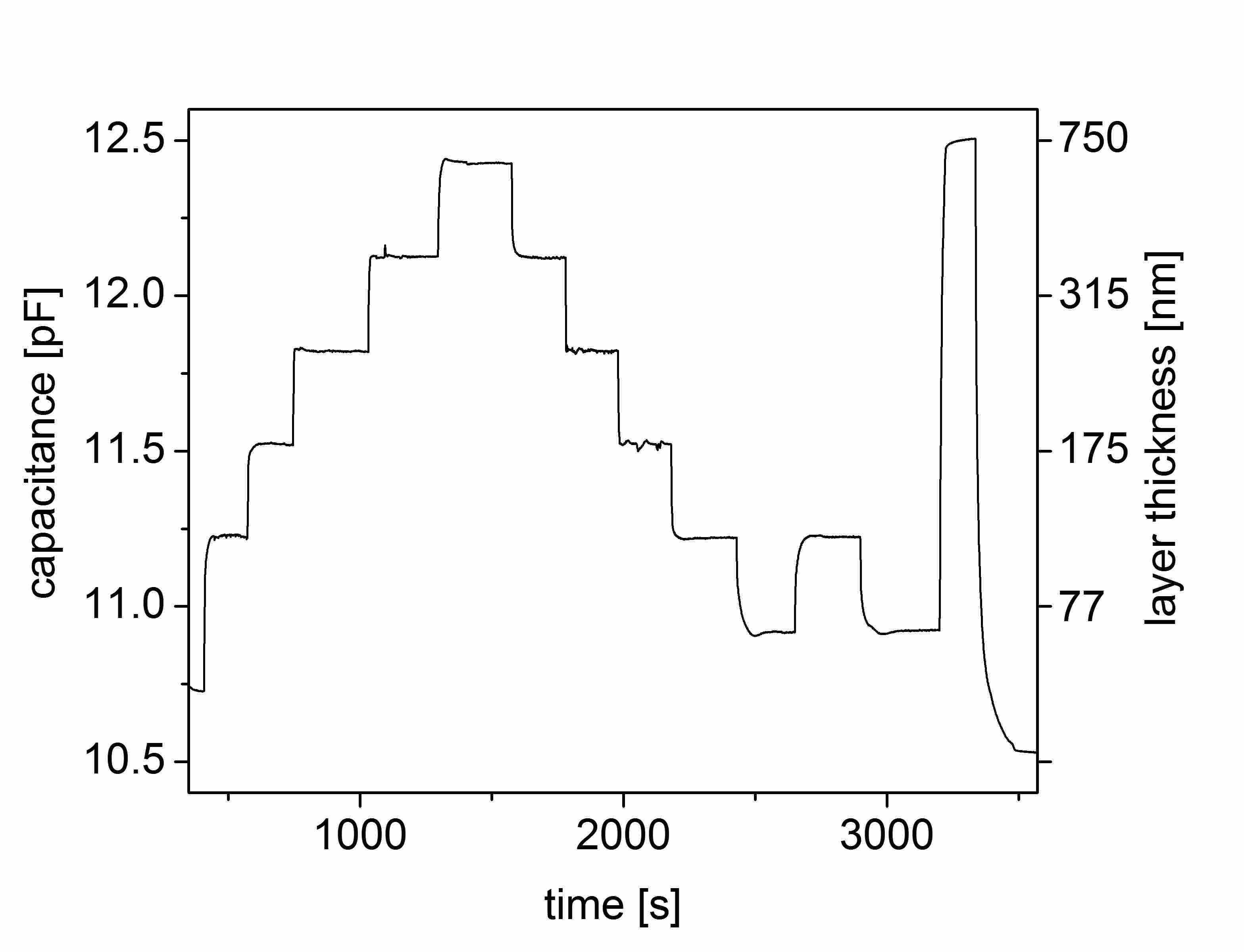
As in the previous case the noise of the measurement is dominated by the PID control loop. Because of the smaller difference in dielectric constant between liquid and solid phases, similar errors on the capacitance result in larger uncertainties in the layer thickness. The layer thickness, as in the previous tests, is calibrated using the FEMLAB simulation, with the dielectric constants appropriate for the LXe environment. The steps in the graph correspond to layer thicknesses of 32.90.4 nm, 119.70.8 nm, 1853 nm, 2622 nm, and 3838 nm, where the error denotes the maximum deviation from the average value over the time the layer is stabilized. The last peak refers to the saturation capacitance of 12.48 pF for solid Xe, while the value of 10.51 pF for pure liquid is measured at the end of the plot. The corresponding sensitivity for 100 nm layers is 38.75 fF/nm for SXe in Xe gas and 6.14 fF/nm for SXe with the sensor immersed in LXe. This measurement reproduces the expected behavior of LXe and SXe with dielectric constants = 1.88 (161.35 K, = 2.98 g/cm3) [13] and = 2.2 (160 K, = 3.54 g/cm3) [19].
In a final test, layers are sublimated in a controlled way to keep the partial pressure of the evaporated gas at a low level. This is important for the EXO experiment, where strict bounds exist on the amount of Xe tolerable in the ion trap vacuum system [6]. The tungsten heater on the back side of the sensor is used to sublimate the layers, while the cryostat is kept cold. The correlation of sublimation rate and pressure in the vacuum system is shown in Fig. 10.
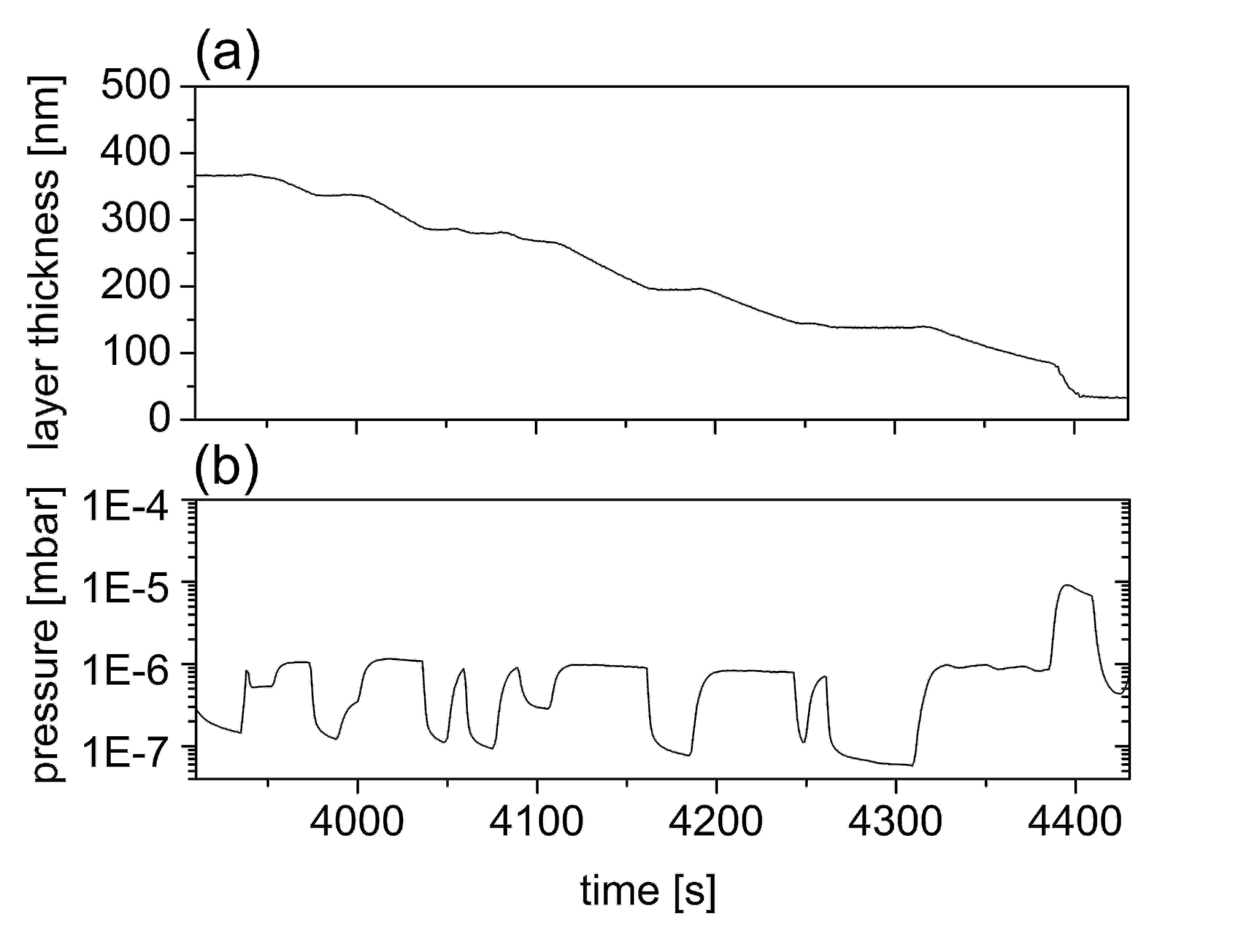
Here, the vacuum chamber with a volume of 1.5 l is pumped with a 70 l/s turbo molecular pump. The plot indicates that an evaporation rate of 2 nm/s results in a partial pressure of 110-6 mbar. Scaled to the EXO ion trap system with a pumping speed of 500 l/s and a volume of 20 l, this corresponds to a partial pressure of 110-8 mbar, well below the acceptable limit of about 510-6 mbar.
6 Conclusion
We have developed a versatile and simple microfabricated sensor for accurate capacitive measurements of thin layers of dielectric substances. The sensor can be calibrated for many substances due to its asymptotic saturation behavior for thick deposited layers. This asymptotic behavior is in good agreement with an electrostatic field simulation and the relative dielectric constant values from the literature. Data was presented for the specific application that led to this development, the controlled growth, stabilization and removal of solid Xe layers in gaseous Xe, liquid and vacuum environments. The sensors presented, with appropriate readout schemes, are capable of controlling solid Xe layers in Xe gas and liquid with sensitivities of 38.75 fFnm and 6.2 fFnm, respectively. Other applications of the sensor include the control of coatings with different dielectric materials from gaseous or liquid environments and the characterization of dielectric emulsions in situations where ruggedness and miniaturization are important.
7 Acknowledgements
The essential support from the staff at the Stanford Nanofabrication Facility is gratefully acknowledged. We also thank B. Young for advice and technical help and D. Osheroff for the loan of the Andeen-Hagerling capacitance bridge. Finally we thank the Agilent Corporation for the loan of one of their E4980A capacitance bridges.
References
- [1] Now at Stanford Linear Accelerator Center, Menlo Park, CA 94025.
- [2] C. Lu, A. W. Czanderna (eds.), Applications of piezoelectric quartz crystal microbalances, Elsevier, Amsterdam (1984).
- [3] M. Breidenbach et al., “EXO: an advanced Enriched Xenon double-beta decay Observatory”, Proposal to SAGENAP, (2000); unpublished.
- [4] J.A. Macdonald, Ed., AIP Conf. Proc. 108 (1984).
- [5] B. Flatt et al., Nucl. Instr. Meth. A, 578, 399 (2007).
- [6] M. Green et al., Phys. Rev. A 76 023404 (2007).
- [7] Application Note 1217-1, ”Basics of Measuring the Dielectric Properties of Materials” Hewlett Packard literature number 5091-3300E, (1992).
- [8] Vespel is a trademark of DuPont.
- [9] Lakeshore Cryotronics Inc., 75 McCorkle Blvd, Westerville, OH 43082, USA.
- [10] National Instruments Corp, 11500 N Mopac Expwy, Austin TX 78759.
- [11] H. Froehlich, Theory of Dielectrics, Clarendon Press, Oxford (1949).
- [12] .
- [13] CRC Handbook of Chemistry and Physics, 87th Edition, CRC Press, Boca Raton (2006).
- [14] E. Petinelli et al., J. Geophys. Res. 108, 101 (2003).
- [15] O. Hilt et al., J. Phys.: Cond. Mat, 6 L735 (1994).
- [16] D. R. Sears et al., J. Chem. Phys., 37 3002 (1962).
- [17] E. H. Kennard, Kinetic Theory of Gases, McGraw-Hill, London (1938).
- [18] REFPROP, NIST standard reference database 23, v.7 (2002).
- [19] M. L. Klein et al., Rare gas solids, Academic Press, London (1976).
| Sensor | Spacing | Thickness | Width | Area | Capacitance |
|---|---|---|---|---|---|
| [m] | [m] | [m] | [mm2] | [pF] | |
| 1 | 1.50 | 1.85 | 0.8 | 0.69 | 7.3 |
| 2 | 1.50 | 1.85 | 2.5 | 0.69 | 4.1 |
| 3 | 1.50 | 1.85 | 5.5 | 0.69 | 3.2 |
| 4 | 1.50 | 1.85 | 11.5 | 0.69 | 2.3 |
| 5 | 1.50 | 1.85 | 0.8 | 2.84 | 23.1 |
| 6 | 1.50 | 1.85 | 2.5 | 2.84 | 14.0 |
| 7 | 1.50 | 1.85 | 5.5 | 2.84 | 11.6 |
| 8 | 1.50 | 1.85 | 11.5 | 2.84 | 9.1 |
| 9 | 1.47 | 2.00 | 2.5 | 2.26 | 23.0 |
| 10 | 1.47 | 2.00 | 1.5 | 2.26 | 28.0 |
| Substance | Csat | Sensitivity | Sensor | Csat/ | |
| [pF] | [fF/nm] | [pF] | |||
| H2O (solid) | 2.400.02 | 7.40.1 | 1 | 3.2[11] | 0.750.01 |
| Xe (liquid) | 1.2600.005 | 3.90.1 | 1 | 1.880 [13] | 0.670.01 |
| Xe (solid, 100 K) | 1.5150.005 | 4.70.1 | 1 | 2.24 [13] | 0.670.01 |
| CO2 (solid) | 1.430.01 | 4.40.1 | 1 | 2.12 [14] | 0.680.01 |
| Xe (solid, 30 K) | 5.2410.005 | 16.30.1 | 6 | 2.25 [15, 16] | 2.330.01 |
| Kr (solid, 30 K) | 4.1180.005 | 12.80.1 | 6 | 1.66 [13] | 2.480.01 |
| Ar (liquid, 87 K) | 3.610.05 | 11.20.2 | 6 | 1.50 [13] | 2.410.03 |
| N2 (liquid, 70 K) | 3.550.05 | 11.00.2 | 6 | 1.45 [13] | 2.440.04 |
| Xe (solid, 15 K) | 5.360.004 | 11.160.01 | 5 | 2.25 [15, 16] | 2.380.01 |
| Xe (solid, 155 K) | 7.9790.003 | 16.620.01 | 9 | 2.20 [15, 16] | 3.590.01 |
| Xe (liquid) | 10.5120.002 | 21.890.01 | 10 | 1.880 [13] | 5.590.02 |
| Xe (solid, 155 K) | 12.4840.002 | 38.750.01 | 10 | 2.20 [15, 16] | 5.620.02 |