Role of semi core levels in determining the band-gaps of semiconductors : First-principles calculations with model Hamiltonians
Abstract
First principle calculations based on LDA/GGA approximation for the exchange functional underestimate the position of the semi core 3 levels in Ga (=N, P and As) semiconductors. A self-interaction correction scheme within the LDA+U/GGA+U approximation is found to be sufficient to correct this discrepancy. A consequence of this correction is that the bandgap () of the semiconductors also improves. The belief has been that the bandgap correction comes from modified semi core-valence interaction. We examine this often used approximation in great detail and find that although bandgap changes as large as 0.63 eV for GaAs, 0.42 eV for GaP and 0.46 eV for GaN are obtained within this approach for = 20 eV on the Ga states, only 0.1 eV, 0.1 eV and 0.15 eV for GaAs, GaP and GaN arise from semi core-valence interaction. As is increased, the bandgap keeps improving. We trace this effect primarily to the interaction of the Ga 4 states in the conduction band with the anion states.
I. Introduction
Enormous progress has been made over the years in the development of realistic theories of materials starting from a first-principles approach real-th . A popular method in this direction is the Kohn-Sham formalism of density functional theory. The Hohenberg-Kohn theorem states kohn that the ground state energy can be written as an exact functional of the density. Unfortunately, the exact form of the functional is not known and approximations such as the local density approximation (LDA) lda ; self-inter as well as the generalised gradient approximation (GGA) ggapw91 ; ggapbe have been used quite successfully in describing the ground state properties of a wide variety of systems. There are however limitations of this method when one attempts to calculate the excited state properties such as the bandgap. The Kohn-Sham band-gaps of semiconductors are smaller than the experimental values. Even if one ignores the fact that the Hohenberg-Kohn theorem is a theory of the ground state, there are limitations coming from the form of the exchange correlation functional. The Kohn-Sham (KS) band-gap E is related to the fundamental band-gap of the solid Eg by the relation where is the discontinuity in the exchange correlation functional exch_corr when an electron is added to the system. and has the corrections due to correlation effects. This discontinuity is lacking in the local density approximation resulting in the equality of the Kohn-Sham and the fundamental bandgap. The second, separate issue is the effect of the approximation of the exchange functional which arises from a spurious self-interaction error self-inter . In addition electron correlation effects are underestimated in density functional theory which leads to the incorrect placement of the levels. For a more detailed discussion of the pros and cons of density functional theory see Ref rmartin .
For bonded semiconductors, the GW approximation gw has been enormously successful in improving the calculated bandgap. In this method, a partially or fully self-consistent solution of the Dyson equation is used to determine the self-energy which provides a correction to the KS-LDA bandgap. Another contributory factor to the gap error is the cation position in semiconductors semicore , especially when these levels are relatively shallow. The levels are not deep enough to be chemically inert and so they interact with the valence band states leading to a reduction of the bandgap. A cheap and rather inexpensive method that has been used in the literature gapcorr ; chris for correcting for the bandgap has been the LDA+U/GGA+U method ldapu1 ; ldapu2 . Within this scheme a potential is introduced on the valence / semi core states which is dependent on the atom and angular momentum projected density operator. This pushes the semi core /valence states to deeper energies and therefore modifies the valence band maximum (VBM) position as a result of the modified semi core-valence / valence interaction.
In this work we have performed a detailed analysis of the GGA+U approach for correcting the bandgap of semiconductors in which a is applied to the cation states. We also studied the changes in the band structure and bandgap as a function of . Aligning all the states with respect to the anion 1 level for that value, we find that at point, apart from movement of the Ga 3 states, the changes are primarily at the valence band maximum. All other states largely remain unshifted. As the semi core states are pushed to deeper energies, there would be a corresponding reduction in the coupling between the semi core and valence states. Hence for largish values of the , the VBM should stop moving. This however does not happen. We examined if this was a consequence of the fact that the potential is angular momentum dependent, but does not distinguish between the ’principal quantum number’ of the state involved. Invoking a description of the eigenfunctions in terms of an atomic description, for GaAs, the potential applied on the Ga states does not distinguish between Ga 3 and Ga 4 states. There is a small admixture of the unoccupied Ga 4 states in the ground state charge density. The applied potential which depends on the Ga density for a given value of , pulls the Ga 4 states to lower energies where they interact more strongly with the As states, therefore increasing the gap. This effect can be controlled by varying the muffin tin radius (RMT) of the sphere about Ga in which the potential is applied. A decreased muffin tin radius would have a reduced Ga 4 component and therefore modifies the potential. However even after reducing the Ga 4 component, the gap keeps increasing although the changes are small. These changes we speculate could arise from modified screening of the states as the states are moved deeper in energy or other modifications in the electronic structure arising from charge reorganization within the Ga states. For the first time we clarify how the bandgap is modified by a on the semi core states. We also provide the band offsets between the =0 and finite results for the GaX. These show that the self-interaction error due to the incorrect placement of the Ga states changes both the valence band offset as well as the conduction band offset. Similar conclusions were found earlier by Janotti et al. chris .
II. Methodology
We have carried out ab-initio calculations within the generalised gradient approximation of density functional theory. A full potential linearized augmented plane wave implementation in the WIEN2K code wien2k was used by us in our calculations. We considered the systems GaN, GaP and GaAs and evaluated the electronic structure at the experimental lattice lattc constants of 4.52, 5.45 and 5.65 respectively. Electronic structure calculations were performed for different muffin tin radii and the reasons for this will be discussed in the text. Unless otherwise stated, the results disscussed will be for RMT= 2.3, 2.2 and 1.8 a.u for Ga in GaAs, GaP and GaN respectively. The radii for As, P and N were kept fixed at 2.3, 2.0 and 1.8 a.u. In the calculations = 12 and RK= 7. The number of k-points used was 64 (4x4x4) for the self-consistency, while a gamma-centered grid of 8x8x8 was considered in the evaluation of the Density of states. The tetrahedron method of integration was used for the DOS calculation. The GGA PW91 approximation ggapw91 to the exchange functional was used. An additional potential within the GGA+U ldapu2 formalism was introduced on the Ga states, and the changes in the electronic structure was calculated as a function of . Further analysis has been carried out within a tight-binding model (discussed later) found to be adequate to give a good description of the electronic structure. This enables us to estimate bandgap shifts coming from various interactions. In addition plane wave pseudopotential calculations vasp , have been carried out using PAW potentials paw . A gamma centered grid of 8x8x8 k-points and GGA-PW91 approximation for the exchange have been used. Superlattices of the form were constructed to determine the valence and conduction band offsets introduced by , measured with respect to the =0 result. The electronic structure of the superlattices was carried out using a plane wave pseudopotential implementation within VASP vasp . A k-points grid of 6x6x1 was used. The positions of the atoms making up the superlattice were fully optimized.
III. Results and discussion
In Fig. 1 we have plotted the , , projected density of states for = 0, 5 and 10 eV for GaAs. As expected the Ga 3 states are pushed deeper into the valence band as is varied. The gross features of the valence band however remain unchanged. Apart from the bandgap underestimation in these calculations that we discussed earlier, another source of error in these calculations is the underestimation in the position of the semi core levels. This is a consequence of the overbinding of states that one finds in LDA-type calculations semicore . Experimentally expt , these levels are found at -17.0, -18.8 and -18.9 eV inside the valence band for GaN, GaP and GaAs.
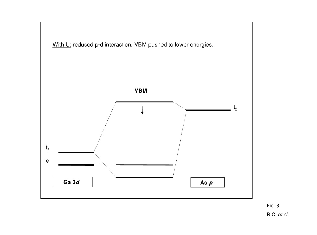
There are however some striking effects on the bandgap as is varied. Considering the example of GaAs, one examines the variation in the bandgap as the position of the semi core states are varied (Fig. 2). The bandgap increases from 0.44 eV to 0.71 eV as is increased from 0 to 9 eV. The first question is why does the bandgap change as the Ga 3 states are pushed deeper into the valence band. This is illustrated schematically in Fig. 3 for the symmetries involved at the point. The energy splitting of the Ga 3 states in the point ion limit is shown in the left panel. One has below . The states on the As interact with the states of Ga 3 and hence form bonding and antibonding states. The VBM position in the absence of Ga 3-As interaction would have been where the unperturbed As derived states are. The interaction leads to a reduction in the bandgap of the semiconductor. Now as the Ga 3 states are pushed deeper into the valence band, one expects the VBM to stop moving at some point where the interaction strength becomes negligibly small.
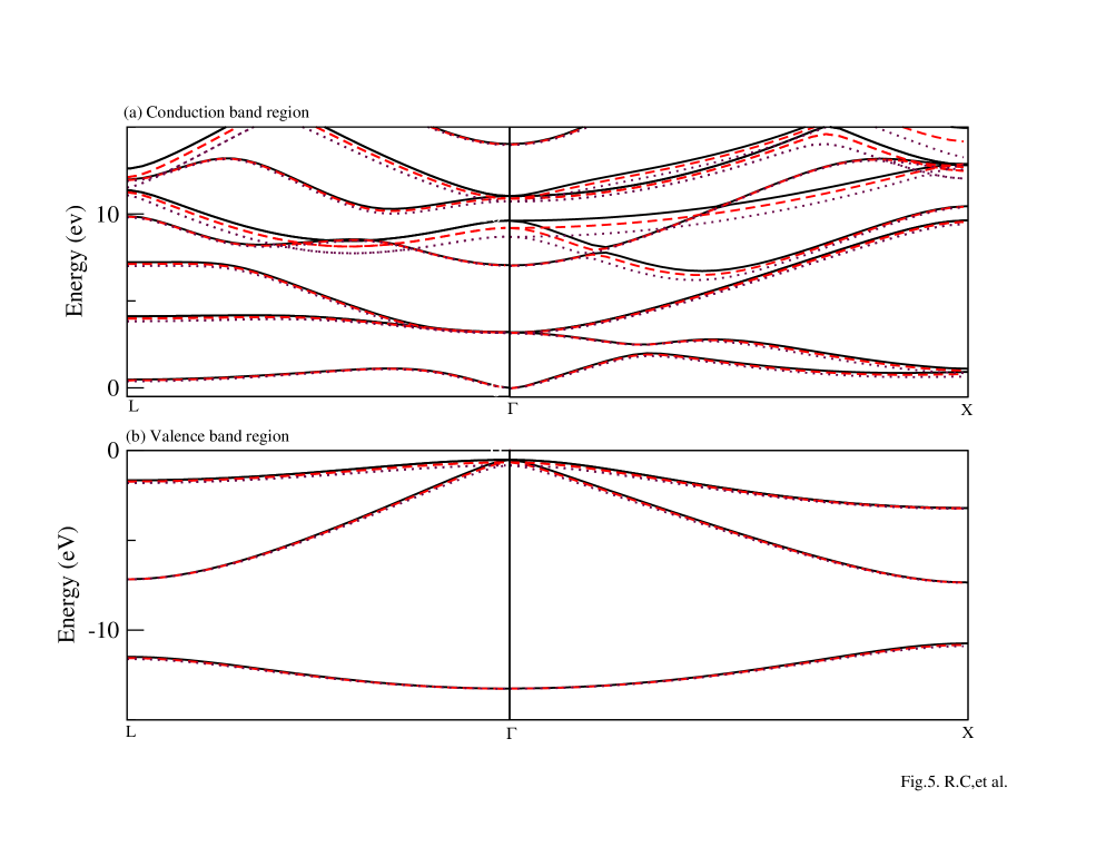
In order to understand this further we have considered a minimal tight-binding model with , and states in the basis for both Ga and As, P. In the case of GaN only , states were included on N. Nearest neighbor interactions between the anion and cation as well as next neighbor interactions between anion pairs and cation pairs have been considered. The comparisons of the band dispersions obtained for GaAs, GaP and GaN from VASP and from TB fitting for the various values are given in Fig.4. The parameters entering the TB Hamiltonian (Table I) have been extracted by fitting the first principle results by a least square error minimization process. The parameters are similar to values present in the literature ddtb . We use the values of the interactions strengths estimated between the semi-core and valence states to estimate the renormalization of the bandgap due to these interactions. This is found to be just 0.1 eV for GaAs and GaP and 0.15 eV for GaN.
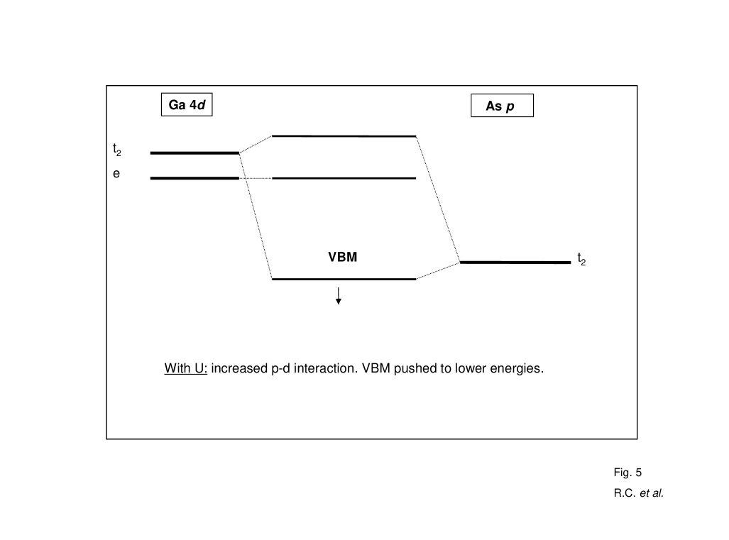
Now as the Ga 3 states are pushed deeper into the valence band, one expects the VBM to stop moving at some point where the interaction strength becomes negligibly small. We have moved the Ga 3 states to absurdly deep energies using say a of 20 eV where we expect the interaction to go to zero. The VBM however does not stop moving. A possible reason for this is the following and is shown schematically in Fig. 5. The introduced potential in the GGA+U ldapu2 formalism is on the Ga admixture in the ground state charge density contained within the sphere of specified mufin tin radius. This does not distinguish between Ga 3 and 4. Hence since the ground state charge density has some Ga 4 admixture, the Ga 4 states are also pulled to lower energies. These interact with the VBM derived As levels and hence modify the bandgap which keeps on increasing with . This is illustrated in Fig. 6 where we show the valence and conduction band structure as is varied. With the changes in the valence band are small, while the changes in the conduction band are substantial. Therefore we clarify for the first time that a part of the observed increase in the bandgap with on the semi core states is because of the interaction of the unoccupied Ga 4 states with the states comprising the VBM.
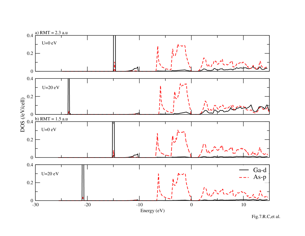
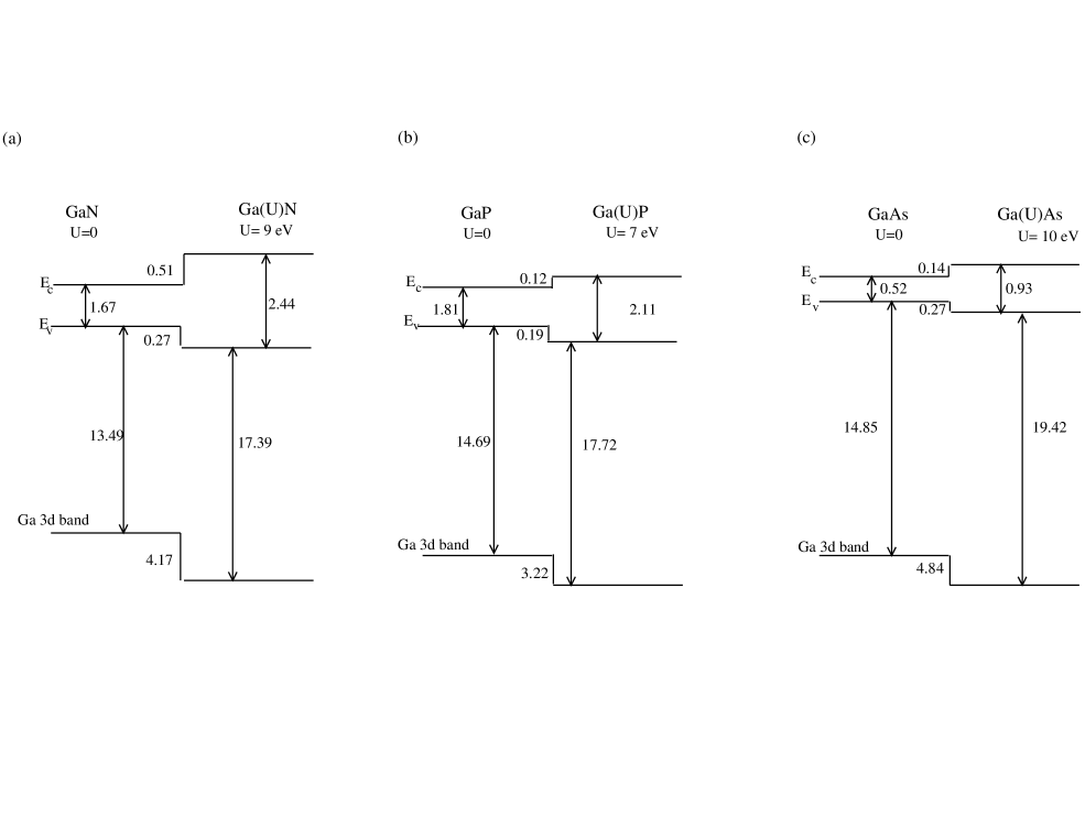
The question we asked next was whether we can reduce the component of the 4 states on which the potential is applied. This has been done by varying the muffin tin radius about the atom on which the potential is applied and the resulting density of states for GaAs are shown in Fig.7. For =0 we find that the large RMT result indicates that there is substantial Ga admixture in the valence band. However as the muffin tin radius is reduced, this contribution is substantially reduced. Hence for large and large RMT we find the unusual result that the Ga states contribution in the valence band increases. We would expect it to decrease by virtue of the fact that we are moving the Ga states deeper. For small RMT however we do not find an increase in the Ga component in the valence band. The modifications in the bandgap with RMT are given in Table II. The changes are small for small RMT, though the bandgap improvement is still larger than what is expected from the tight binding model. We examine what the modifications of the electronic structure are as a function of with a smaller muffin tin radius of 1.5 a.u. Aligning the different calculations with respect to the anion 1 for the same , we find that the relative separtion of the anion core levels remain unchanged while those of the Ga core levels are strongly modified. This is given in Table III. From this we infer that there is no charge transfer taking place between Ga and X. However the charge on the Ga gets reorganised between the levels resulting in a change in the relative separations of the core levels. This observation is consistent with the fact that there are modifications of the charge on the Ga atoms, while that on the anions is essentially unchanged. Hence as a function of , there are changes in the Ga--anion- interactions which results in substantial modifications of the bandgap. However there is no change in the effective charge transfer between the anion and cations sites as function of . Constructing a superlattice of the form we determine the valence band and conduction band offsets between the =0 and finite results. Here the value has been chosen so that we obtain agreement in the position of the experimental Ga 3 positions. These are shown in Fig. 8. We find that a on the semicore state shifts the conduction band minimum as well as the valence band maximum to different extends. These conclusions are similar to those obtained by Janotti et al. chris .
In contrast to the LAPW method where the region over which the GGA+U correction is applied is controlled by the choice of the muffin tin radius, such a freedom does not exist in pseudopotential calculations. We have calculated the change in the bandgap for the GaN, GaP and GaAs within a pseudopotential approach (Table IV). The results are similar to our large RMT results.
In Fig. 9 we have plotted the variation of the approximate position of the Ga 3 states with respect to the VBM as a function of . The behaviour is almost linear and we use this plot to determine the value of that will bring about agreement with experiment for the Ga 3 states. Hence a of approximately 11, 14 and 13 eV, with a muffin tin radius of 1.5 a.u, for GaN, GaP and GaAs respectively is found to be sufficient to bring about agreement with experiment. Similar range of was required to get the position of the states correct in ZnO clas-zno . We would however like to point out that GGA+U is basis set dependent and therefore the value (for obtaining a certain effect) differs between different computational methods, different choice of muffin-tin radius, etc.
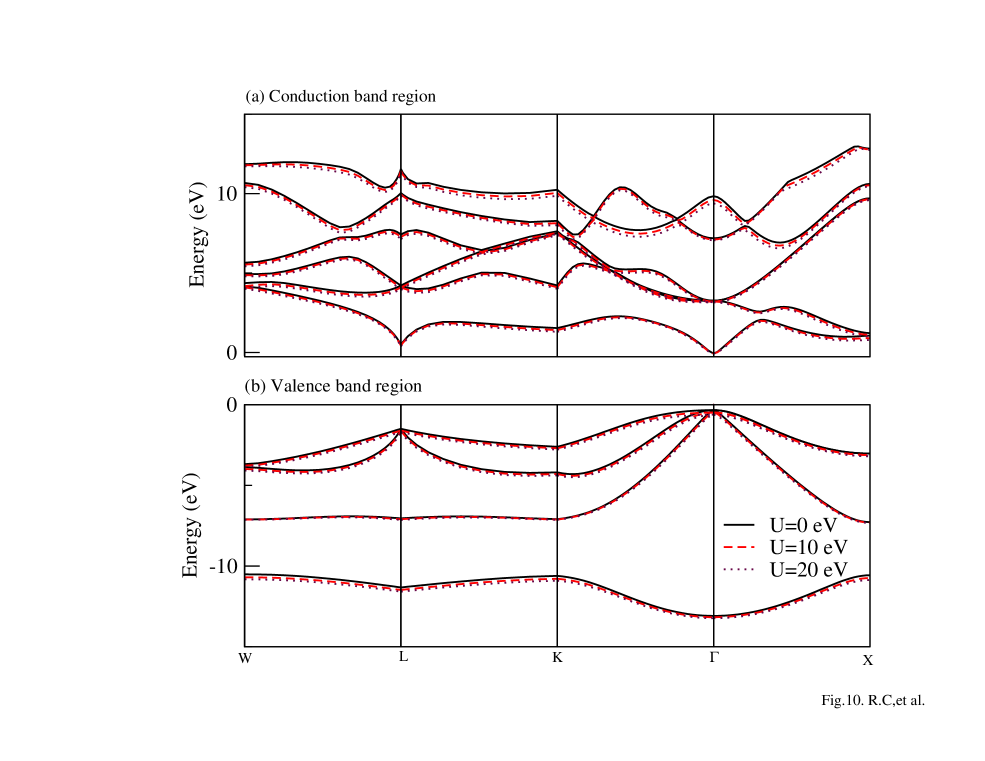
In Fig. 10 we have plotted the variation in the band structure of the valence band as well as the conduction band region for GaAs as a function of for a smaller muffin tin radius of 1.5 a.u. The conduction band minimum has been defined as the zero of the energy scale. There are dependent changes in the electronic structure that one finds. A popular method used in the correction of the band-gap of semiconductors is one in which all the states are rigidly shifted scissor . This method results in a constant shift of a band at all points, which is indeed not the case as evident from Fig. 10. Hence a -dependent self energy is intrinsic to the GGA+U approach which involves a self consistent solution of the Kohn-Sham Hamiltonian in the presence of the additional potential. This has been pointed out by Persson and Mirbt bjphy who explain that LDA underestimates the -point electron and light-hole masses due to a too strong k-dependent bonding-antibonding interaction; the heavy-hole and spin-orbit split off masses are in general less affected by this interaction. This LDA failure is very apparant for GaAs where LDA produces a very small bandgap, and the corresponding LDA average masses (see Ref. persson2 for definition of the geometric average masses) are = 0.01, = 0.49, = 0.02, and = 0.07, whereas the experimental values expt-mass are = 0.07, = 0.53-0.59, = 0.08, and = 0.13. The k-dependent modifications in the GGA+U formalism result in an increase of the bandgap and also a weakening of the bonding-antibonding interaction, thereby improving the effective masses. Using the LAPW method with = 9 eV we obtain = 0.04, = 0.62, = 0.05, and = 0.12 which agree much better with the measured values.
IV. Conclusion
To conclude, we have examined a popular and computationally inexpensive method of correcting for the bandgap underestimation in first-principle calculations. For small values of one finds that the changes in the valence band are confined to the region around the point. Suprisingly there are changes induced in the unoccupied states as well, as a function of on the semi-core states. This has been pointed out as arising from the fact that the GGA+U potential is applied on the admixture in the ground state charge density. This can be reduced by choosing a smaller muffin tin radius for the atom to which GGA+U corrections are applied. Another component to the bandgap increase is from modified screening of the valence states as the Ga semi-core states are pushed deeper into the valence band.
PM thanks DAE-BRNS, India for financial support under project number 2005/37/8/BRNS. We all thank the Swedish Research Council (VR), and the Swedish Foundation for International Cooperation in Research and Higher Education (STINT).
References
- (1) R.O. Jones and O. Gunnarsson, Rev. Mod. Phys. 61, 689 (1989).
- (2) P. Hohenberg and W. Kohn, Phys. Rev 136, 864 (1964).
- (3) D.M. Ceperley and B.J. Alder, Phys. Rev. Lett. 45, 566 (1980) as parametrised by J.P. Perdew and Zunger in self-inter .
- (4) J.P. Perdew and A. Zunger, Phys. Rev B 23, 5048 (1981).
- (5) J.P. Perdew and Y. Wang, Phys. Rev. B 45, 13244 (1992).
- (6) J.P. Perdew, K. Burke and M. Ernzerhof, Phys. Rev. Lett. 77, 3865 (1996).
- (7) J.P. Perdew and M. Levy, Phys. Rev. Lett. 51, 1884 (1983); L.J. Sham and M. Schlter, Phys. Rev. Lett. 51, 1888 (1983).
- (8) R.M. Martin, Electronic Structure: Basic Theory and Practical Methods (Cambridge University Press, 2004)
- (9) F. Aryasetiawan and O. Gunnarsson, Rep. Prog. Phys. 61, 237 (1998).
- (10) S. H. Wei and A. Zunger, Phys. Rev. B 37, 8958 (1988); P. Schrer, P. Krger and J. Pollmann, Phys. Rev. B 47, 6971 (1993); P. Schrer, P. Krger and J. Pollmann, Phys. Rev. B 48, 18264 (1993); S. B. Zhang, S. H. Wei and A. Zunger, Phys. Rev. B 52, 13975 (1995).
- (11) S. Picozzi, M. Lezaic and S. Blgel, cond-mat 0603589 ; S. Zh. Karazhanov, P. Ravindran, U. Grossner, A. Kjekhus, H. Fjellvag, B. G. Svensson, J. Cryst. Growth 287 162 (2006); S. Zh. Karazhanov, P. Ravindran, U. Grossner, A. Kjekshus, H. Fjellvag, B. G. Svensson, J. Appl. Phys. 100, 043709 (2006)
- (12) Anderson Janotti, David Segev, and Chris G. Van de Walle, Phys. Rev. B 74, 045202 (2006).
- (13) V.I. Anisimov, I.V. Solovyev, M.A. Korotin, M.T. Czyzyk and G.A. Sawatzky, Phys. Rev. B 48, 16929 (1993). A. I. Liechtenstein, V. I. Anisimov and J. Zaanen, Phys. Rev. B 52, R5467 (1995).
- (14) S. L. Dudarev, G. A. Botton, S. Y. Savrasov, C. J. Humphreys and A. P. Sutton, Phys. Rev. B 57, 1505 (1998).
- (15) P. Blaha, K. Schwartz, G. K. H. Madsen, D. Kvasnicka and J. Luitz; An Augmented Plane Wave + Local Orbitals Program for calculating crystal properties (K. Schwarz, Techn. University Wien, Austria, 2001), ISBN 3-9501031-1-2.
- (16) J. Singh, Physics of Semiconductors and Their Heterostructures (McGraw-Hill, New York, 1993); T. Lei, T. D. Moustakas, R. J. Graham, Y. He, and S. J. Berkowitz, J. Appl. Phys. 71, 4933 (1992).
- (17) G. Kresse and J. Furthmller, Phys. Rev. B. 54, 11169 (1996); G. Kresse and J. Furthmller, Comput. Mat. Sci. 6, 15 (1996).
- (18) P.E. Blochl, Phys. Rev. B 50, 17953 (1994); G. Kresse, and J. Joubert,Phys. Rev. B 59, 1758 (1999).
- (19) N.J Shevchick, J. Tejeda, and M. Cardona, Phys. Rev. B 9, 2627 (1971); G. Martin, A. Botchkarev, A. Rockett, and M. Morkoc, Appl. Phys. Lett. 68, 2521 (1996).
- (20) R. Viswanatha, S. Sapra, T. Saha-Dasgupta and D.D. Sarma, Phys. Rev. B 72, 045333 (2005).
- (21) C. L. Dong, C. Persson, L. Vayssieres, A. Augustsson, T. Schmitt, M. Mattesini, R. Ahuja, C. L. Chang, and J.-H. Guo, Phys. Rev. B 70, 195325 (2004).
- (22) G.A. Baraff and M. Schlter, Phys. Rev. B 30, 3460 (1984).
- (23) C. Persson and S. Mirbt, Br. J. Phys. 36, (2006) (in press).
- (24) C. Persson and U. Lindefelt, J. Appl. Phys. 82, 5496 (1997).
- (25) Numerical Data and Functional Relationships in Science and Technology, New Series, Vol. III/17a,b, edited by O. Madelung et al., (Springer, Berlin, 1982).


| GaN | GaP | GaAs | |
|---|---|---|---|
| sc | 6.696 | 1.82 | 1.01 |
| pc | 9.49 | 7.94 | 6.59 |
| dc | -13.16 | -14.46 | -14.74 |
| sa | -12.97 | -8.59 | -9.97 |
| pa | -0.92 | -0.46 | -0.367 |
| da | - | 7.71 | 6.88 |
| scsa | -1.42 | -1.59 | -1.33 |
| scpa | 3.28 | 2.76 | 2.67 |
| scda | - | -2.07 | -1.72 |
| pcpa | 3.17 | 2.85 | 2.94 |
| pcpa | -0.92 | -1.05 | -0.81 |
| pcda | - | -0.62 | -0.50 |
| pcda | - | 1.60 | 1.28 |
| dcda | - | 0.0 | 0.0 |
| dcda | - | 0.0 | 0.0 |
| dcda | - | 0.0 | 0.0 |
| pcsa | -0.28 | -1.54 | -0.75 |
| dcsa | -0.77 | 0.0 | 0.0 |
| dcpa | 1.08 | 0.636 | 0.568 |
| dcpa | -0.01 | -0.224 | -0.318 |
| scsc | -0.59 | -0.31 | -0.26 |
| scpc | 0.69 | 0.46 | 0.05 |
| scdc | -0.06 | -0.22 | -0.16 |
| pcpc | 1.49 | 0.11 | 0.28 |
| pcpc | 0.0 | -0.04 | -0.23 |
| pcdc | 0.0 | 0.0 | 0.0 |
| pcdc | 0.0 | 0.03 | 0.0 |
| dcdc | -0.06 | -0.01 | 0.0 |
| GaN | GaP | GaAs | |
|---|---|---|---|
| dcpa | -0.01 | -0.224 | -0.318 |
| scsc | -0.59 | -0.31 | -0.26 |
| scpc | 0.69 | 0.46 | 0.05 |
| scdc | -0.06 | -0.22 | -0.16 |
| pcpc | 1.49 | 0.11 | 0.28 |
| pcpc | 0.0 | -0.04 | -0.23 |
| pcdc | 0.0 | 0.0 | 0.0 |
| pcdc | 0.0 | 0.03 | 0.0 |
| dcdc | -0.06 | -0.01 | 0.0 |
| dcdc | 0.02 | 0.01 | 0.01 |
| dcdc | 0.0 | 0.0 | 0.0 |
| sasa | -0.06 | 0.0 | -0.01 |
| sapa | 0.2 | 0.0 | 0.07 |
| sada | - | -0.15 | -0.13 |
| papa | 0.34 | 0.23 | 0.31 |
| papa | -0.05 | -0.05 | -0.04 |
| pada | - | -0.24 | -0.31 |
| pada | - | 0.15 | 0.13 |
| dada | - | -0.98 | -0.84 |
| dada | - | 0.51 | 0.43 |
| dada | - | -0.1 | -0.036 |
| RMT (a.u) | Bandgap change (eV) | |
|---|---|---|
| GaN | 1.8 | 0.46 |
| GaN | 1.5 | 0.34 |
| GaP | 2.0 | 0.42 |
| GaP | 1.5 | 0.29 |
| GaAs | 2.3 | 0.63 |
| GaAs | 1.5 | 0.29 |
| Core level | U (eV) | |||
| 10 | 20 | |||
| GaN | ||||
| Ga | 1S1/2 | -723.683948 | -723.581975 | |
| Ga | 2S1/2 | -64.611804 | -64.501480 | |
| Ga | 2P1/2 | -53.981829 | -53.871907 | |
| Ga | 2P3/2 | -51.947788 | -51.837825 | |
| Ga | 3S1/2 | 17.218648 | 17.295227 | |
| Ga | 3P1/2 | 20.651111 | 20.725591 | |
| Ga | 3P3/2 | 20.912098 | 20.985360 | |
| N | 1S1/2 | 0.0 | 0.0 | |
| GaP | ||||
| Ga | 1S1/2 | -598.619678 | -598.517630 | |
| Ga | 2S1/2 | 60.447143 | 60.558034 | |
| Ga | 2P1/2 | 71.077537 | 71.187967 | |
| Ga | 2P3/2 | 73.111528 | 73.222006 | |
| Ga | 3S1/2 | 142.286256 | 142.362896 | |
| Ga | 3P1/2 | 145.719349 | 145.793838 | |
| Ga | 3P3/2 | 145.980772 | 146.054018 | |
| P | 1S1/2 | 0.0 | 0.0 | |
| P | 2S1/2 | 140.426058 | 140.424829 | |
| P | 2P1/2 | 144.012722 | 144.011600 | |
| P | 2P3/2 | 144.080163 | 144.079036 | |
| Core level | U (eV) | |||
|---|---|---|---|---|
| 10 | 20 | |||
| GaAs | ||||
| Ga | 1S1/2 | 109.385718 | 109.544887 | |
| Ga | 2S1/2 | 768.448458 | 768.620852 | |
| Ga | 2P1/2 | 779.078965 | 779.250701 | |
| Ga | 2P3/2 | 781.112945 | 781.284749 | |
| Ga | 3S1/2 | 850.307135 | 850.427101 | |
| Ga | 3P1/2 | 853.741405 | 853.858096 | |
| Ga | 3P3/2 | 854.003530 | 854.118328 | |
| As | 1S1/2 | 0.0 | 0.0 | |
| As | 2S1/2 | 752.001092 | 752.000418 | |
| As | 2P1/2 | 763.627530 | 763.626944 | |
| As | 2P3/2 | 766.316562 | 766.315964 | |
| As | 3S1/2 | 847.269176 | 847.268283 | |
| As | 3P1/2 | 851.175282 | 851.174383 | |
| As | 3P3/2 | 851.544909 | 851.544006 | |
| (eV) | Bandgap (eV) | |
|---|---|---|
| GaN | 0 | 1.633 |
| GaN | 5 | 1.758 |
| GaN | 10 | 1.875 |
| GaN | 20 | 2.095 |
| GaP | 0 | 1.742 |
| GaP | 5 | 1.846 |
| GaP | 10 | 1.948 |
| GaP | 20 | 2.157 |
| GaAs | 0 | 0.438 |
| GaAs | 5 | 0.576 |
| GaAs | 10 | 0.725 |
| GaAs | 20 | 1.068 |