Photonic-crystal slabs with a triangular lattice of triangular holes
investigated
using a guided-mode expansion method
Abstract
According to a recent proposal [S. Takayama et al., Appl. Phys. Lett. 87, 061107 (2005)], the triangular lattice of triangular air holes may allow to achieve a complete photonic band gap in two-dimensional photonic crystal slabs. In this work we present a systematic theoretical study of this photonic lattice in a high-index membrane, and a comparison with the conventional triangular lattice of circular holes, by means of the guided-mode expansion method whose detailed formulation is described here. Photonic mode dispersion below and above the light line, gap maps, and intrinsic diffraction losses of quasi-guided modes are calculated for the periodic lattice as well as for line- and point-defects defined therein. The main results are summarized as follows: (i) the triangular lattice of triangular holes does indeed have a complete photonic band gap for the fundamental guided mode, but the useful region is generally limited by the presence of second-order waveguide modes; (ii) the lattice may support the usual photonic band gap for even modes (quasi-TE polarization) and several band gaps for odd modes (quasi-TM polarization), which could be tuned in order to achieve doubly-resonant frequency conversion between an even mode at the fundamental frequency and an odd mode at the second-harmonic frequency; (iii) diffraction losses of quasi-guided modes in the triangular lattices with circular and triangular holes, and in line-defect waveguides or point-defect cavities based on these geometries, are comparable. The results point to the interest of the triangular lattice of triangular holes for nonlinear optics, and show the usefulness of the guided-mode expansion method for calculating photonic band dispersion and diffraction losses, especially for higher-lying photonic modes.
pacs:
42.70.Qs, 42.82.Et, 78.20.Bh, 42.65.KyI Introduction
Photonic crystals (PhC) embedded in planar waveguides, also called PhC slabs, are at the heart of current research on photonic crystalsjoanno ; sakoda ; johnson ; inoue ; busch ; lourtioz because of the possibility of confining light in all spatial directions combined with the advantage of a lithographic definition of the pattern. The propagation of light in these systems can be controlled by a two-dimensional (2D) photonic lattice in the waveguide plane, and by total internal reflection in the perpendicular direction. Waveguides with strong refractive index contrast (like the suspended membrane, or air bridge) support truly guided modes lying below the light line dispersion in the cladding materials.russell95 ; krauss96 ; johnson99 ; chutinan00 ; johnson00 ; qiu02 ; notomi02 ; whittaker02 However, most of the photonic modes (or all of them, in the case of waveguides with weak refractive index contrast) lie above the light line and are only quasi-guided, as they are subject to intrinsic losses due to out-of-plane diffraction.lalanne01 ; palamaru01 ; ochiai01-fdtd ; ochiai01-pert ; lalanne02 ; hadley02 ; fan02 ; tikhodeev02 ; morand03 ; ferrini03 ; cryan05
The physical properties of PhC slabs can be significantly different from those of the corresponding 2D system, for several reasons. First, the 2D photonic modes are subject to confinement in the vertical waveguide and the resulting blue shift is strongly polarization-dependent. Second, the presence of second- and higher-order waveguide modes can produce a complicated pattern of photonic bands, especially for higher-lying states. Third, diffraction losses of quasi-guided modes are an inherent feature of PhC slabs which is absent in the ideal 2D case. For all of these reasons, some basic and well-known properties of 2D photonic crystals cannot be easily translated to PhC slabs. For example, it is well known that the triangular lattice of circular air holes in 2D supports a complete photonic band gap for all propagation directions and light polarizations at sufficiently large air fractions.joanno ; meade92 ; villeneuve92 ; gerard94 Nevertheless, the same lattice realized in a high-index membrane does not possess a complete band gap, as the odd modes with respect to a horizontal mirror plane (often called quasi-TM modes) are subject to a strong and non-uniform blue shift which eliminates the gap.johnson99 ; andreani02_ieee Indeed, most applications of PhC slabs employ the even modes (often called quasi-TE), which do possess a band gap for all propagation directions.
It was recently suggestedtakayama05 that the triangular lattice of triangular air holes in a high-index membrane gives rise to a complete photonic gap for both even and odd modes. The physical mechanism is the reduction of symmetry of the basis in the unit cell, as compared to the hexagonal symmetry of the 2D lattice, giving rise to a splitting between the first and the second odd bands at the K point of the Brillouin zone: when realized in a high-index membrane, this gap overlaps the usual gap between the first and the second even bands, giving rise to a complete gap for all directions and polarizations. The experimental results reported in Ref. takayama05, support the existence of a complete photonic gap.
A main purpose of this paper is to perform a systematic study of the triangular lattice of triangular holes, as compared to the triangular lattice of circular holes, both being realized in a high-index dielectric membrane. We calculate the photonic band dispersion, gap maps, and intrinsic losses of quasi-guided modes for the 2D lattice. We also treat line-defect waveguides obtained by removing a full row of holes, and point cavities consisting of three missing holes. In addition to a determination of photonic gaps for even and odd modes as a function of membrane thickness and air fraction, we compare diffraction losses for the lattices with conventional (circular) and reduced symmetry (triangular) holes: this comparison is important in order to assess the possible usefulness of the reduced-symmetry lattice. Among the results, we find interesting prospects of the triangular lattice of triangular holes for nonlinear optics, as it may allow to achieve doubly-resonant second-harmonic generation (SHG) with an even (quasi-TE) fundamental wave and an odd (quasi-TM) harmonic wave when line-defect waveguides or photonic cavities are introduced.
The calculations reported in this paper are performed with an approach which we name Guided-Mode Expansion (GME) method. Maxwell equations are treated by expanding the magnetic field into the basis of guided modes of an effective homogeneous waveguide, and by solving the resulting eigenvalue equation numerically. Intrinsic losses of quasi-guided modes are obtained by calculating the coupling to leaky modes of the effective waveguide within perturbation theory (i.e., the photonic analog of Fermi Golden Rule for quantum-mechanical problems). The GME method, although being an approximate one (since the basis of guided modes is not a complete basis set), has been applied to a variety of photonic lattices and has proven to be useful especially for obtaining quasi-guided modes and their diffraction losses.andreani02_ieee ; andreani02_pss ; andreani03_apl ; gerace04_pre ; gerace04_pss ; andreani04_pn ; gerace05_oqe It has also been successfully employed for the interpretation of optical experiments on PhC slabs.patrini02 ; galli02_epjb ; malvezzi03 ; galli04 ; galli05_jsac ; galli05_prb ; gerace05_apl Another purpose of this paper is to provide a detailed description of the GME method, together with convergence tests and exemplifying applications.
The rest of this work is organized as follows. In Section II we outline the GME method and discuss a few convergence tests. Section III contains the results for the 2D triangular lattice of triangular holes in a high-index membrane, namely photonic dispersion, gap maps and intrinsic losses. In Sec. IV we present a few results for line-defect waveguides and point cavities in the triangular lattice of triangular holes. Section V contains a discussion of the results and of prospective applications of the investigated lattice. Technical details, which are needed by the reader in order to implement the GME method, are given in the Appendices.
II Guided-mode expansion method
As PhC slabs are intermediate between 2D photonic crystals and dielectric slab waveguides, it is reasonable to describe photonic modes in these systems starting from slab waveguide modes and introducing the effect of a dielectric modulation in the core and cladding layers. This is the central idea of the guided-mode expansion method, in which PhC slab modes are expanded in the basis of guided modes of an effective homogeneous waveguide and coupling to radiative modes is taken into account by perturbation theory. In this Section we describe the formalism for calculating mode dispersion and intrinsic losses, for the general case of an asymmetric PhC slab, and discuss convergence of the method.
II.1 Formalism for photonic dispersion
The system we are considering is shown in Fig. 1a. It consists of a PhC slab made of three layers 1,2,3, each of which is homogeneous in the vertical () direction and is patterned with a 2D photonic lattice in the plane. The core layer has a thickness , while the lower and upper claddings are taken to be semi-infinite.note:semi-infinite Patterning of each layer is characterized by the same 2D Bravais lattice, while the basis in the unit cell can be different - a typical situation is that the core layer 2 is patterned, while layers 1 and 3 are not (i.e., they can be described by the same Bravais lattice as layer 2, but with a vanishing air fraction). Writing , the dielectric constant is piecewise constant in the direction and takes the form in each layer . We assume a magnetic permeability .
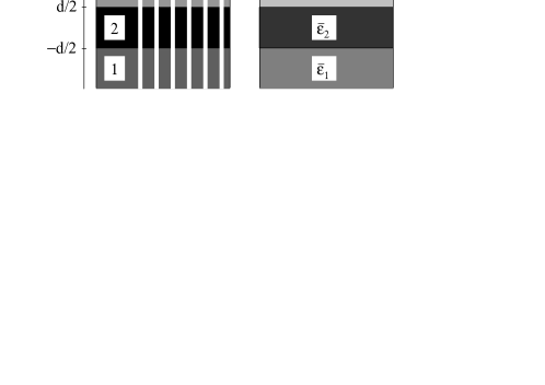
As is well known, Maxwell equations for the electric and magnetic fields E, H with harmonic time dependence can be transformed into the second-order equation for the magnetic field
| (1) |
with the condition . By expanding the magnetic field in an orthonormal set of basis states as
| (2) |
the orthonormality condition being expressed by
| (3) |
Eq. (1) becomes equivalent to a linear eigenvalue problem
| (4) |
where the matrix is given by
| (5) |
This formulation of the electromagnetic problem bears strong analogies to the quantum-mechanical treatment of electrons, with the hermitian matrix playing the role of a quantum Hamiltonian. Once the magnetic field of a photonic mode is known, the electric field can be obtained from
| (6) |
and the electric field eigenmodes are orthonormal according to
| (7) |
as is well knowncarniglia71 and easily verified.
In order to define an appropriate basis set for the expansion (2), we introduce an effective slab waveguide made of three homogeneous layers with dielectric constants , , , as illustrated in Fig. 1b. We take as the spatial average of in each layer:
| (8) |
where the integral extends over a unit cell of area . This choice for the average dielectric constants is convenient, but by no means unique - numerical tests and other issues related to the choice of are discussed in Subsec. II.3. In any case, we assume that the average dielectric constants fulfill the inequalities
| (9) |
in order for the effective slab to support a set of guided modes. Their explicit form is well knownyariv_book and it will be summarized here in order to specify our notation, as well as for the paper to be self-contained. Let us denote by the 2D wavevector in the plane with modulus and unit vector , by a unit vector perpendicular to both g and , and by the frequency of a guided mode which satisfies . Moreover we define the following quantities:
| (10) | |||||
| (11) | |||||
| (12) |
which represent the real (imaginary) parts of the wavevector in the core (upper/lower cladding), respectively. The guided mode frequencies are found by solving the following implicit equations (with the suffix being understood for simplicity):
| (13) |
for transverse electric (TE) polarization, and
| (14) |
for transverse magnetic (TM) polarization. The guided modes at a given wavevector g are labelled by the index and the eigenfrequencies are denoted by . Explicit forms for the electric and magnetic fields of the guided modes are given in Appendix A, as they are needed for the calculation of the matrix elements (5).
The guided modes of the effective waveguide in Fig. 1b depend on a wavevector g which can take any value in the 2D plane. However, photonic modes in the PhC slab of Fig. 1a have the form dictated by Bloch-Floquet theorem and they depend on a wavevector k which is usually restricted to the first Brillouin zone of the 2D lattice: indeed, the effect of the dielectric modulation is to fold the guided modes of the effective waveguide to the first Brillouin zone and to produce photonic bands and band gaps. We therefore write , where the Bloch vector k lies in the first Brillouin zone and G is a reciprocal lattice vector. As the basis states for the expansion (2) of the magnetic field, we choose the guided modes of the effective waveguide given in Appendix A. The guided-mode expansion of the magnetic field therefore readsnote:alpha
| (15) |
The basis set is orthonormal according to Eq. (3), but not complete, since the radiative modes of the effective waveguide are not included in the basis set. This approximation will be partially lifted in Sec. II.2, where the effect of radiative modes in determining diffraction losses will be taken into account.
With this choice for the basis set, the general index can be written as . The matrix elements of Eq. (5) can be calculated in a straightforward way from the field profiles of the guided modes: the resulting analytic expressions are somewhat lengthy and are given in Appendix B. They depend on the inverse dielectric matrices
| (16) |
in the various layers. Like in usual 2D plane wave calculations, a numerically convenient approach to calculate these matrix elements is to define the dielectric matrix
| (17) |
and to find by numerical matrix inversion as : this procedure is known to have much better convergence properties as a function of the number of plane waves,ho90 ; lalanne96 since the truncation rules for Fourier series in the presence of discontinuous functions are better represented.li96 If the photonic lattices in layers 1–3 have a center of inversion (the same for all layers), the dielectric matrices , are symmetric in and turns out to be a real, symmetric matrix when the phases of the fields are chosen as in Appendix A. In the most general case of a photonic lattice without a center of inversion (like the triangular lattice with triangular holes investigated in this work), the matrix is complex hermitian. Line and point defects can be treated by introducing a supercell in one or two directions, respectively, like in 2D plane-wave calculations.
The formalism presented here refers to the most general case of an asymmetric PhC slab. If the structure is symmetric under reflection by a horizontal mirror plane [i.e., if the upper and lower claddings have the same dielectric pattern and are made of the same dielectric materials, ], the basis states as well as the photonic eigenmodes can be classified as even or odd with respect to the mirror plane. We denote by the corresponding specular reflection operator and we shall refer to even (odd) states with respect to this operator as () modes. The simplest way to exploit this mirror symmetry is to solve the eigenvalue problem (4) separately for and states by keeping only the appropriate solutions of Eqs. (13),(14), as detailed in Appendix C. There we also discuss the issue of polarization mixing in the framework of the GME method: in general, a photonic mode of a PhC slab is a superposition of TE-polarized and TM-polarized basis states and all six components of the electric and magnetic fields are usually non-vanishing. Another useful symmetry property holds when the Bloch vector k lies along special symmetry directions, for which mirror reflection with respect to a vertical plane () is a symmetry operation of the PhC slab: in this case the eigenmodes can be classified as even or odd with respect to this mirror symmetry, i.e., they have or respectively. Vertical mirror symmetry can be exploited by transforming the matrix with a unitary transformation which decouples the blocks corresponding to states.
II.2 Formalism for intrinsic losses
When a photonic mode in the PhC slab falls above the cladding light line (or light lines, if the waveguide is asymmetric), it is coupled to leaky modes of the slab by the dielectric modulation and it becomes quasi-guided, i.e., it is subject to intrinsic losses due to scattering out of the plane. The losses can be represented by an imaginary part of the frequency , which is related to the Q-factor of a resonance by .
Within the GME method, the imaginary part of frequency can be calculated by time-dependent perturbation theory, like in Fermi Golden Rule for quantum mechanics. The imaginary part of the squared frequency of a PhC mode with Bloch vector k, whose frequency lies above the cladding light lines (or at least above one of them), is given by
| (18) |
where the matrix element between a guided and a leaky PhC slab mode is given by
| (19) |
and is the 1D photonic density of states (DOS) at fixed in-plane wave vector for radiation states that are outgoing in medium :
| (20) | |||||
Notice the sum over reciprocal lattice vectors and polarizations in Eq. (18), as all diffraction processes contribute to . Equations (18)–(20) generalize the expressions given in Ref. ochiai01-pert, to the case of an asymmetric PhC slab and to situations in which processes with all contribute to diffraction losses. Once is found, the imaginary part of frequency is easily obtained as .
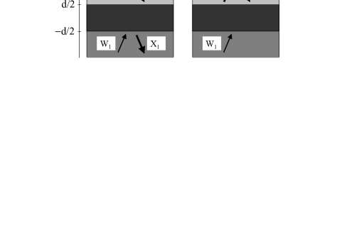
For a given wavevector g and polarization of the radiative modes, there are two scattering channels, corresponding to states with an outgoing component in the lower cladding (medium 1) or in the upper cladding (medium 3).carniglia71 ; note:outgoing The radiation modes are schematically shown in Fig. 2. The state which is outgoing in medium 1 corresponds to a photonic DOS with in Eq. (20), while the outgoing state in medium 3 corresponds to a DOS with . Radiation states are normalized according to Eq. (3), and only the field components in the cladding regions are relevant in determining the normalization. note:normalization Since the field profile of a scattering state tends to a plane-wave form in the far field, the photonic density of states (20) is appropriate whatever the explicit field profile of radiative PhC slab modes. In the present GME method, we evaluate the matrix element by approximating the radiation modes of the PhC slab with those of the effective waveguide. This approximation is consistent with the treatment of the previous Subsection, as the set of guided+radiation modes of the effective waveguide is orthonormal according to Eq. (3), and will be shown later to yield accurate results for diffraction losses when compared to more exact methods. In Appendix D we give the explicit form of radiation states of the effective waveguide which are outgoing in either the lower cladding (Fig. 2a) or in the upper cladding (Fig. 2b), for both TE and TM polarizations. Using expansion (15) for the magnetic field of a PhC slab mode, the matrix element (19) becomes
| (21) |
where
| (22) |
are matrix elements between guided and radiation modes of the effective waveguide, which can be calculated analytically. In Appendix E we collect the matrix elements (22), for all possible combinations of polarizations. Those expressions are implemented together with Eqs. (18)–(22), in order to evaluate the imaginary part of frequency and hence the intrinsic diffraction losses of quasi-guided modes.
The calculation of losses is computationally more demanding than the photonic dispersion alone, as the eigenvectors of the linear problem (4) are also needed. The formalism for intrinsic diffraction losses presented in this Subsection and in the Appendix refers to the general case of an asymmetric PhC slab. If the slab is symmetric, and if the PhC slab modes are found as states as outlined in Appendix C, it is possible to define and use symmetric or antisymmetric outgoing states instead of the scattering states illustrated in Fig. 2. If this is done, () quasi-guided modes are coupled only to symmetric (antisymmetric) radiative states. From a computational point of view there is no special advantage in using symmetry-adapted radiative states, as the computing time needed to implement the perturbative formula Eq. (18) is usually small. Thus even in the case of a symmetric PhC slab it is convenient to use the general loss formalism, and simply obtain or PhC slab states by selecting the basis states of the effective waveguide, as explained in Appendix C.
II.3 Discussion of the method
In this Subsection we discuss the convergence properties of the GME as a function of numerical parameters and give a brief overview of previously published results and comparison with other approaches. Truncation parameters in the GME method are the choice and number of plane waves and the number of guided modes of the effective waveguide kept in the expansion. The dimension of the eigenvalue problem (4) is , or about half of this value when vertical parity is used. The choice of plane waves can be made in analogy to usual 2D plane-wave expansion: the important point is how to calculate the inverse dielectric matrix properly, as already noticed in Subsec. II.1. In the present implementation we take an isotropic cutoff for reciprocal lattice vectors and adopt the common procedure of inverting the dielectric matrix numerically:ho90 while this is adequate for many purposes, improved implementations of the plane-wave expansion lalanne98 ; david06 could also be introduced in the GME method in order to speed up convergence.
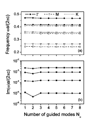
The optimal depends on waveguide parameters and on the frequency region considered: typically, for PhC slabs defined in a thin high-index membrane, in each parity sector (i.e., for both and modes) yields very accurate results for the lower-lying modes. As an example, in Fig. 3 we show the real and imaginary parts of the frequency for a few photonic modes as a function of the number of guided modes , for modes in the triangular lattice of circular air holes. Structure parameters are similar to those used later in the paper. The number of plane waves is truncated to , which is sufficient for convergence in the present lattice. It can be seen that both the mode energies and the imaginary parts are stable for , while a good approximation is obtained already for or even . This is very convenient for the purpose of design and search of parameters, as a photonic structure in a high-index contrast PhC slab can be optimized within a fully 3D approach, with the same computing time of a conventional 2D plane-wave expansion. The precise calculation (e.g., with ) can be performed a posteriori once the structure parameters are optimized.
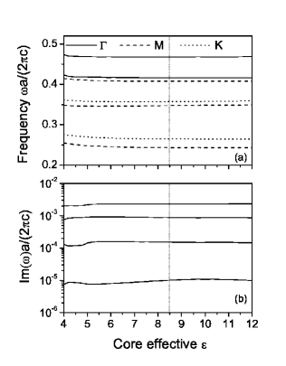
It is also important to discuss the choice of the dielectric constant of the effective waveguide, which is usually taken to be the spatial average (8) in each layer. While this choice is a natural one, it might be asked whether the results depend on the assumed value of . In Fig. 4 we show the real and imaginary parts of frequency for a few modes, with the same parameters of the previous Figure, as a function of the effective dielectric constant in the core region. It can be seen that the results are rather insensitive to the assumed value of , except when it becomes smaller than about five. All curves are flat around the value which corresponds to the spatial average. This satisfactory behavior arises because the GME method employs the set of all guided modes of the effective waveguide (although in practice they are truncated to a finite number for numerical convenience), thereby compensating for different choices of the effective waveguide used to define the basis set. Thus the choice of the dielectric constant of the effective waveguide as the spatial average of is justified, at least for the low air fractions that are commonly employed. Although one might consider extending the method by introducing an anisotropic dielectric tensor for each layer of the effective waveguide, Fig. 4 strongly suggests that the results of the GME method would not be changed by such a complicated extension which is therefore unnecessary.
The approximations of the GME method are: (i) for photonic dispersion, the shift of guided and quasi-guided modes due to second-order coupling to leaky modes of the effective waveguide is neglected; (ii) for diffraction losses, the density of radiative modes of the PhC slab is approximated with that of the effective waveguide. The effect of these approximations can be judged by comparing the results with those of other methods that are known to be exact within numerical accuracy. A full analysis of this issue is outside the scope of this paper, however comparisons between the results of GME and those obtained by other methods have already been published and are shortly summarized here. The dispersion of quasi-guided modes was found to be in very good agreement with the resonance positions in reflectance or transmittance spectra found from a scattering-matrix treatment.andreani02_ieee In fact, the complex frequencies of photonic modes can be obtained from the poles of a scattering matrix.lalanne02 ; tikhodeev02 ; morand03 The intrinsic propagation losses of line-defect waveguides in the triangular lattice obtained with different methods (GME,andreani03_apl finite-difference time-domain or FDTDcryan05 and from the poles of a scattering matrixlalanne02 ; sauvan05_thesis ) were compared for the same waveguide parameters and were found to agree very well with each other: a detailed comparison is presented in Ref. sauvan05_thesis, . A comparative study of GME and Fourier modal methods applied to cavity modes in one-dimensional PhC slabs has been reported in Ref. gerace05_oqe, , and very good agreement was found for the photonic dispersion as well as the intrinsic losses. Finally, the Q-factors of cavity modes in L1, L2 and L3 nanocavities (one, two or three missing holes in the triangular lattice) as a function of nearby hole displacement are found to be almost identical when calculated with either the GME methodandreani04_pn or the poles of a scattering matrix.sauvan05_prb Agreement with experiments performed on PhC slabs made of Silicon-on-Insulator,patrini02 ; galli04 ; galli05_jsac Si membranes,galli05_prb GaAs/AlGaAs,galli02_epjb ; malvezzi03 and Silicon Nitridegerace05_apl is also very satisfactory. The set of these comparisons indicates that the GME is a reliable method for both photonic mode dispersion and intrinsic losses, whose main advantages are computational efficiency and ease of application to various kinds of vertical waveguides and of photonic lattices, both periodic in 2D and containing line- and point defects.
III Triangular lattice with triangular holes
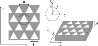
We report in this Section a systematic study of the triangular lattice of triangular air holes patterned on a free-standing high-index slab of thickness , as schematically shown in Fig. 5. The relevant dimensions of this lattice are the triangular basis side, , and the slab thickness. Throughout this Section we assume (unless otherwise specified) that the lattice is patterned in a material with dielectric constant , which is appropriate for Silicon at the usual telecom wavelength m but also to other materials with similar dielectric constants (e.g., GaAs). For the calculations shown in the present Section, we employed up to 109 plane waves and 4 guided modes per parity sector in the basis set of the GME method. All the calculations have been done on an ordinary Pentium computer with low computational effort. The complex Fourier transform of the dielectric constant for the triangular lattice of triangular holes is given in Appendix F. Notice that the lattice is invariant under rotations by and is not centrosymmetric, but since by time-reversal symmetry, the same symmetry directions of the usual triangular lattice of circular air holes do apply.
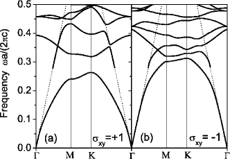
The first realization of such a lattice has been reported in Ref. takayama05, , with the purpose of measuring a complete photonic band gap in a waveguide-embedded 2D PhC thanks to a reduction of symmetry for the basis in the unit cell of the triangular lattice, as already pointed out in the Introduction. The importance of finding a complete photonic band gap in a waveguide-embedded photonic structure is related to the practical realization of linear waveguides or cavities with reduced losses or higher Q-factors, as scattering into quasi-guided modes of opposite parity would be avoided. In Fig. 6 we present the photonic band dispersion calculated with the GME method for structure parameters as in Ref. takayama05, . Even (TE-like) and odd (TM-like) modes are reported in Figs. 6a and b, respectively. It is worth noticing that in the absence of second-order waveguide modes, the fundamental gaps of both parities would overlap in the dimensionless frequency range 0.31-0.32, as it can be seen from the Figure. However, the presence of a second-order mode with cut-off around for both polarizations, as shown in Fig. 6, prevents the opening of a true photonic band gap. Such second-order modes (which do not appear in a 2D treatment with an effective index) are unavoidable in the present structure, due to the relatively large slab thickness, .
We believe that our result is not in contrast with the experimental findings reported in Ref. takayama05, , in which a strong reduction of the transmission intensity was measured along the K and M directions. Since the dispersion of the second-order waveguide mode is very close to the air light line in the relevant frequency region, such modes are barely coupled to the external beam focused on the sample side and also they are subject to large disorder-induced losses; thus, it is likely that transmission into such modes is attenuated in a few lattice periods, which would explain the apparent photonic band gap observed experimentally. On the other hand, when line- or point-defects are introduced, such second-order modes are necessarily present within the gap, thus limiting the usefulness of this design for applications. In the following, we will consider a photonic band gap for the waveguide-embedded structure only when no higher-order modes are present within the apparent gaps formed by the fundamental modes, i.e., when the PhC slab is truly single-mode.
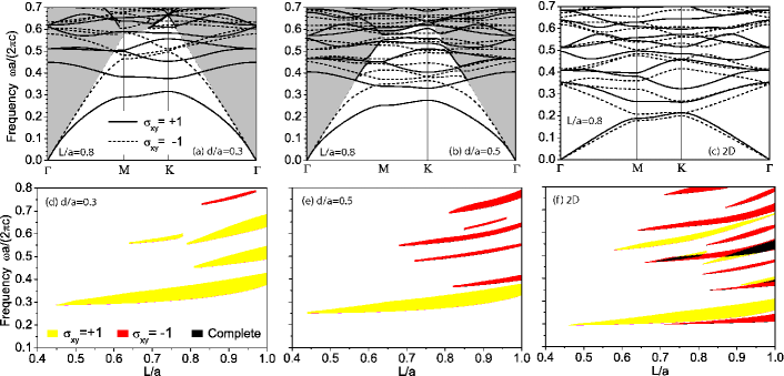
With the aim of optimizing the design proposed by Takayama et al., we performed a systematic study of the present photonic lattice at varying structure parameters. In Fig. 7 we show the photonic band dispersion and gap maps for the triangular lattice of triangular air holes with slab thickness (Figs. 7a and d), (Figs. 7b and e), and for the reference 2D system of infinite thickness (Figs. 7c and f), respectively. As is well known for more conventional lattices, johnson99 ; andreani02_ieee the blue shift of photonic modes with respect to the ideal 2D system due to the dielectric confinement is strongly polarization-dependent; in particular, it is more pronounced for odd (TM-like) modes. This physical behavior is seen by comparing Figs. 7a-c, in which the dispersion of photonic modes is calculated for the same 2D photonic lattice in which triangular air holes have side . For the second-order cut-off is rather high in energy, thus the system can be considered as single-mode below the light line. On increasing the slab thickness, the second-order cut-off red shifts. For , both even and odd modes open their fundamental band gaps, but they do not overlap to give a complete photonic band gap for all symmetry directions. In order to span a wider range of structure parameters, important information can be inferred by the gap width as a function of the holes’ side. As it can be seen in Figs. 7d-f, the gap maps depend strongly on the waveguide thickness and differ substantially from those of the 2D system. For , the fundamental odd gap is closed for all values of , due to the larger blue shift of band edges at the K-point than at the M-point. Even if both fundamental band gaps are present for , no complete gap opens due to the stronger blue shift of odd modes. For , the presence of higher-order modes prevents the opening of complete gaps as well. The gap map for the ideal 2D system presents a great variety of photonic gaps for both polarizations, and also some complete gaps at high frequencies. It is worth noting that the fundamental TE and TM band gaps do not overlap in frequency, unlike in the ordinary triangular lattice of circular air holes.joanno Furthermore, the fundamental TE gap turns out to be narrower than the usual gap for circular holes.
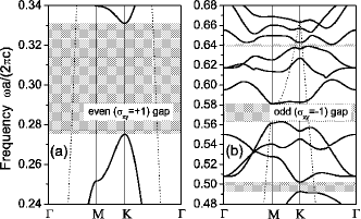
Even if no truly complete band gaps appear to be present for this waveguide-embedded lattice, it is interesting to investigate the formation of resonant gaps at and , to be exploited in non-linear optical applications like second-harmonic generation (SHG). While doubly-resonant SHG has been widely studied in one-dimensional systems like multilayers and microcavities,berger97 ; simonneau97 ; centini99 ; deangelis01 ; dumeige02 ; liscidini04apl ; ochiai05 ; liscidini06pre no 2D photonic lattice giving such an interesting result has been reported in the literature. In particular, it can be seen from Fig. 7e that many odd gaps are present for a slab thickness . In this case, it is easy to find a condition for which the fundamental gap at pump frequency is resonant with a gap at . One of the possibilities is indeed shown in Fig. 8. It is substantially the same result reported in Fig. 7b, but here the odd modes (Fig. 8b) are plotted in a doubled frequency range with respect to the even modes (Fig. 8a). As it can be seen, there is a good overlap in frequency between the large band gap of Fig. 8a and the rather narrow but robust gap of Fig. 8b. This could be interesting, e.g., for applications to non-linear optical converters based on GaAs, in which the pump s-polarized field would be converted into a p-polarized second-harmonic field.note:SHG In this respect, the usefulness of the present lattice would be enhanced with ad hoc fabricated line- or point-defects. It should be reminded that these results have been obtained by using the same dielectric constant for both pump and second-harmonic modes, but it is easy to extend the present calculations to non-linear materials with optical constants of known frequency dispersion.
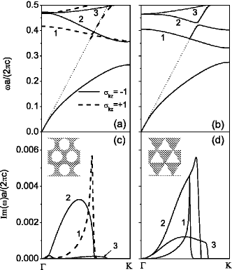
One of the issues when dealing with the triangular lattice of triangular holes would be given by intrinsic losses. In order to show the general interest of the triangular hole-based lattice, and also to show an application of the GME method, we compare intrinsic losses of the present system to the ones of an ordinary circular hole-based PhC slab. In this case, we restrict our discussion to modes along the K symmetry direction. Intrinsic losses are quantified by calculating the imaginary part of frequency, as detailed in the previous Section. In Fig. 9a and c we show the photonic dispersion and intrinsic losses for the first few bands of an ordinary PhC slab with a triangular lattice of circular holes. It can be noticed that the modes along the chosen symmetry direction are separated according to their mirror symmetry with respect to the vertical plane, which can be either even () or odd ().note:sakoda On the right hand side, in Fig. 9b and d, we plot dispersion and losses for the case of triangular holes. In this case no symmetry operation holds, so the modes are mixed. The choice of for the circular holes and for triangular ones, respectively, allows to obtain roughly the same air fraction for the two lattices. This can be also verified by the roughly equal second-order cut-offs. The dispersion is only slightly modified when changing the hole shape from circular to triangular, and in particular it appears that a general blue shift occurs for the modes in Fig. 9b with respect to the ones in 9a. For what concerns intrinsic losses, we can see that they remain almost of the same order on going from circular to triangular holes, at least for the lower frequency bands. This means that (in the absence of disorder) no particular differences are introduced by changing the basis of the lattice, apart from the loss of symmetry . As the band labelled with 1 is almost unchanged on going from the circular to the triangular hole shape, also the intrinsic losses are quite similar between the two lattices. For higher lying bands, in particular for the band labelled with 2, such similarity becomes less evident on approaching the light line, owing to the blue shift of modes for the triangular hole-based lattice and to the mixing with other modes which does not occur in the conventional lattice. In particular, owing to the lack of symmetry, there is an anticrossing between mode 2 and the second-order waveguide mode occurring very close to the light line, which correspondingly affects the imaginary part of frequency (see Figs. 9b-d). The mode labelled with 3 has larger losses for triangular holes than for circular ones, but it is quite high in energy.
As a conclusion to this section, we have shown that the triangular lattice of triangular air holes does indeed have a complete photonic band gap between the fundamental waveguide modes, but the gap is actually eliminated by the presence of second-order modes. The lattice can be designed for nonlinear optical applications in order to have a gap for even modes at the pump frequency which is resonant with a gap for odd modes at the SH frequency. Intrinsic losses are of the same order as in the circular hole-based triangular lattice. The GME method is useful for a comparison of the two lattices and for the design of structures with desired characteristics.
IV Line-defect waveguides and point cavities
We show in the present Section that line- and point-defects can be introduced into the triangular-hole lattice without any loss of performance with respect to the circular-hole one. It is well known that removing a row of holes in a 2D photonic lattice introduces a linear defect supporting guided modes within the photonic band gap. In a triangular lattice such waveguide is usually called W1, and its channel width (namely the distance between the holes surrounding the waveguide) is . These guided modes exploit the usual index confinement along the vertical direction added to the gap confinement in the waveguide plane, and they are studied with great interest by the scientific community owing to prospective applications in photonic integrated circuits.
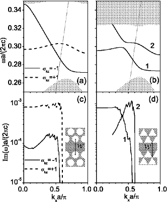
In Fig. 10 we report a comparison between the W1 waveguide realized in the triangular lattice with circular (Figs. 10a-c) and triangular holes (Figs. 10b-d), respectively. For the circular hole-lattice the guided modes are classified according to their mirror symmetry with respect to the vertical plane . For such calculations, we used supercells along the M direction of widths ranging from to , with 181 to 323 plane waves and 4 guided modes in the basis set for the expansion. Then, an average was taken to get final results for losses, in order to smooth out finite supercell effects.andreani03_apl As it is seen from the Figure, the dispersion of the guided modes is very similar between the two systems, apart in the region of mixing. In fact, as is a symmetry operation for the system in Fig. 10a, the two guided modes are completely decoupled, while in Fig. 10b they mix producing a consistent anti-crossing and a mini-gap. Looking at the imaginary part of frequency, we see by comparing Figs. 10c and d that they are almost identical away from the mixing region, which means that W1 waveguides in triangular lattice of triangular holes may behave as standard W1 waveguides.note:proploss Such result is quite surprising, as the asymmetry of such a waveguide could be expected to lead to higher scattering of propagating light states. On the contrary, the reduction of symmetry does not increase losses in the perfect photonic lattice - of course, the role of fabrication imperfections may affect differently the two structures in real lattices.
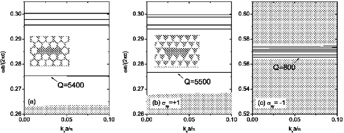
The final goal of this paper is to exploit the potential of the triangular lattice of triangular holes for non-linear optical applications. In this respect, the ultimate system for frequency conversion at the nanoscale is a photonic cavity with double resonance for pump and harmonic waves. Doubly-resonant microcavities for second-harmonic generation have been studied in the context of Fabry-Perot cavities.berger97 ; simonneau97 ; liscidini04apl ; ochiai05 ; liscidini06pre According to a recent proposal, double resonance in photonic crystal cavities may allow to achieve strong coupling between single photons.irvine06 It has been shown that full 3D confinement of light with a very high figure of merit (quality factor, Q) can be achieved by properly designed point-defects in 2D PhC slabs.akahane03 In particular, removing three holes along the K direction (L3 cavity) and optimizing the positions of the holes surrounding the cavity allows to achieve Q-factors of the order of .akahane05 We compare here the L3 cavity structure made in a triangular lattice of triangular air holes to the usual L3 cavity with circular holes and the results are shown in Fig. 11. For such calculations, a square supercell of dimensions has been taken. Up to 1551 plane waves and two guided modes were used in the GME. As it can be seen from Fig. 11a, many dispersionless defect modes appear in the photonic band gap, due to the tight confinement provided by the cavity. We can evaluate the vertical Q-factor of such modes (i.e., the one determined by intrinsic out-of-plane losses) by the definition , where both and have been averaged over the folded Brillouin zone in order to reduce the effects of a finite supercell size. Very good agreement with measured Q-factors and defect mode energies has been already found with this GME-based procedure.andreani04_pn The Q-factor of the un-optimized L3 cavity in the lattice of circular holes is theoretically estimated to be . When the same cavity is realized in the triangular lattice of triangular holes (Fig. 11b), we see that the fundamental mode is almost unchanged, and its Q-factor is comparable to the one of Fig. 11a. The slight blue shift of the defect mode and of the lower band edge in Fig. 11b with respect to Fig. 11a is due to the slightly different air fractions of the two lattices. As we have already shown in Fig. 8, we can design a triangular lattice with triangular holes having a doubly-resonant band gap. Thus, we plot in Fig. 11c the dispersion of modes within the doubled frequency range with respect to Fig. 11b, in analogy with Fig. 8. Many defect modes appear within the band gap, and the lowest mode has a Q-factor of almost , which is a very promising value considering that the structure has not been optimized in any way. There is, in fact, much room for improving the Q-factors at both and by means of geometry optimization of the nearby holes. The present result make us confident that high-Q, doubly-resonant nanocavities may be realized in PhC slabs made of non-linear materials, bringing new exciting results in integrated optics at nanoscale level.
V Conclusions
The triangular lattice of triangular holes in a high-index dielectric slab has been thoroughly investigated by means of the guided-mode expansion method, whose detailed formulation and examples of applications have been given in the paper. The investigated lattice does have a complete band gap for both polarizations when the fundamental waveguide mode is considered, consistently with the results of Ref. takayama05, , but the gap is actually eliminated by the presence of second-order waveguide modes. The intrinsic losses of quasi-guided modes in the triangular lattice with triangular and circular holes, and in line-defect waveguides as well as nanocavities defined therein, are comparable.
An interesting application of the triangular lattice of triangular holes for nonlinear optics follows from the fact that a gap for (TE-like) modes at the pump frequency can be designed to be in resonance with a gap for (TM-like) modes at the harmonic frequency: thus, resonant second-harmonic generation exploiting band-edge effects may be realized. Promising results are also found for point cavities: the L3 cavity in the triangular lattice of triangular holes supports a cavity mode at which can be resonant with a cavity mode at . There is much room for improving the design of doubly-resonant, high-Q nanocavities by geometry optimization. These results are interesting in view of application of the triangular lattice of triangular holes for nanoscale nonlinear optical processes.
Acknowledgments
The authors are grateful to M. Agio, H. Benisty, D. Cassagne, Ph. Lalanne, M. Le Vassor d’Yerville, M. Liscidini, and C. Sauvan for useful conversations and suggestions. They also would like to acknowledge K. Hennessy and W.T.M. Irvine for providing them with the preprint of Ref. irvine06, prior to its publication, thereby motivating the search for doubly resonant PhC cavities. This work was supported by MIUR through Cofin project “Silicon-based photonic crystals for the control of light propagation and emission” and FIRB project “Miniaturized electron and photon systems”, as well as by CNR-INFM through PRA PHOTONIC.
Appendix A Guided modes of the effective waveguide
The frequencies of the guided modes of the effective waveguide are found from the implicit equations (13) for TE polarization, and (14) for TM polarization. The guided modes are labelled by the wavevector g and the mode index ,note:alpha which can be combined into a single index . The mode profiles for TE polarization can be written as follows (with the time dependence being understood), with reference to the geometry of Fig. 1:
| (23) |
| (24) |
In the above expressions, is a normalization surface, which disappears from the final results, while the magnetic field is obtained from the electric field thorugh the Maxwell equation . Application of standard transfer-matrix theory leads to the following relations between coefficients (with the suffix being understood for simplicity):
| (25) | |||||
| (26) | |||||
and to the well known implicit equation (13) of the main text. The normalization integral (3) implies the relation
| (28) |
which, together with Eqs. (25)–(LABEL:eq:tecoeff3), determines all coefficients and .
The guided modes for TM polarization are characterized by the following field profiles:
| (29) |
| (30) |
where the electric field follows from the magnetic field profile through Eq. (6). The appropriate relations between coefficients can be derived from (25)-(LABEL:eq:tecoeff3) by the replacements , and , (except in the trigonometric functions), . The normalization integral of the magnetic field gives the condition
| (31) |
Appendix B Matrix elements for photonic dispersion
We calculate the matrix elements of Eq. (5) between guided modes of the effective waveguide from the field profiles given in Appendix A for TE and TM polarizations. We adopt the following notations: and , where k is the Bloch-Floquet vector, G and are reciprocal lattice vectors and , are the indices of guided modes of the effective waveguide at wavevectors , respectively. There are four kinds of matrix elements: TE-TE, TM-TM, TE-TM and TM-TE. The integral in Eq. (5) can be broken into three terms over the regions 1,2,3 where the dielectric constant does not depend on , and can be expressed in terms of the following integrals:
The integrals in Eq. (5) yield the inverse dielectric matrices in the three layers, , defined in Eq. (16). The matrix elements are then obtained as follows:
| (33) |
| (34) |
| (35) |
Appendix C Symmetry properties and TE/TM mixing
If the PhC slab is invariant under reflection through a mirror plane bisecting the slab (which we take as ), the effective waveguide has the same reflection symmetry and its eigenmodes can be classified as even or odd with respect to the reflection operator defined in the main text. The spatial symmetries of the nonvanishing field components are given in Table 1, assuming a wavevector along the direction. The guided mode frequencies are found from the following implicit equations:
| (36) | |||||
| (37) | |||||
| (38) | |||||
| (39) |
Notice that the first-order TE and TM modes of the effective waveguide are described by Eqs. (36) and (39), respectively. By keeping only () basis states in the guided-mode expansion, photonic eigenmodes which are even (odd) with respect to horizontal mirror symmetry are obtained, and the computational effort in solving the eigenvalue equation (4) is reduced.
| * | * | * | ||||
| * | * | * | ||||
| * | * | * | ||||
| * | * | * |
In general, a photonic eigenmode in a PhC slab is a linear combination of TE- and TM-polarized basis states and all six components of the electric and magnetic field are nonvanishing. Nevertheless, low-lying photonic modes are often dominated by the lowest-order guided mode of the effective waveguide. In this situation, states are dominated by the TE guided modes described by Eq. (36) and can be called “quasi-TE”, while states are dominated by the TM guided modes described by Eq. (39) and can be called “quasi-TM”. This widespread terminology is useful and appropriate for large wavevectors, when the dominant field components are the spatially even ones: making reference to Table 1, and since the dielectric modulation couples guided modes with all wavevector directions in the 2D plane, the dominant components are (for or TE-like modes) or (for or TM-like modes). However, the terminology becomes inadequate when the PhC slab is multimode, as it always happens at sufficiently high frequencies. If the waveguide is not symmetric, any PhC slab mode is a linear combination of basis states arising from all equations (36)–(39) and even the lowest-order TE/TM guided modes of the effective waveguide are mixed.
Appendix D Radiation modes of the effective waveguide
In this Appendix we give the radiation modes of the effective waveguide which are outgoing in either the lower or the upper cladding (see Fig. 2). Each of these radiation modes is labelled by the wavevector g in the 2D plane, the frequency , and the polarization. In the following the quantum numbers will be understood in order to simplify the notations. Instead of distinguishing between real and imaginary components of the wavevectors in the three regions as in Eq. (12), we define three complex wavevectors as
| (40) |
While the wavevector in the core region is always real, the wavevectors in the cladding regions can be either real or purely imaginary according to the values of the dielectric constants and of . If the effective waveguide is symmetric () all radiation modes have real , while if there is a frequency region in which is real but is imaginary: i.e., a quasi-guided mode in this region of - space is diffracted to the lower (but not to the upper) cladding. This phenomenon is automatically taken into account by the Kronecker -function in the DOS formula (20), as the photonic DOS vanishes when is imaginary. Therefore we shall write down the electric and magnetic field components of radiative waveguide modes assuming that all ’s are real - if one of them is purely imaginary, that radiation mode does not carry an energy flux and it does not contribute to scattering loss.
With this proviso, the radiation modes of the effective waveguide for TE polarization in the three regions can be written as follows (setting , , and with the time dependence being understood):
| (41) |
| (42) | |||||
For the scattering state which is outgoing in the lower cladding (Fig. 2a), and the normalization condition (3) determines the coefficient of the outgoing componentnote:scattering as . All other coefficients are then found from a standard transfer-matrix calculation, which yields
| (43) |
and
| (44) |
On the other hand, for the state outgoing in the upper cladding (Fig. 2b), and the proper normalization conditionnote:scattering is . The other coefficients can then be found from the inverse relations of (43), (44).
For what concerns TM-polarized radiation modes, the field profiles are given by
| (45) |
| (46) | |||||
For the scattering state outgoing in the lower cladding (Fig. 2a), and the normalization condition (3) determines the coefficient of the outgoing component as . For the state outgoing in the upper cladding (Fig. 2b), and the proper normalization condition is . All other coefficients can be found from transfer-matrix theory, the relevant expressions being obtained from (43), (44) by the replacements , and (except in the exponential functions).
Appendix E Matrix elements for diffraction losses
We calculate the matrix elements (22) between guided and radiation modes of the effective waveguide, to be used in formula (21) for the loss calculation. The expressions are similar to those of Appendix B, but care must be taken to distinguish between the different quantum numbers. Guided modes are labelled by the wavevector and by the index , which are combined as before into a single index . Radiation modes are labelled by the wavevector , the frequency , the polarization , and an additional index which specifies whether the mode is outgoing in medium 1 or 3: all these quantum numbers will be grouped into a single index . Like for the matrix elements between guided modes, there are four possible combinations of polarizations. The integral can be broken into three terms over the regions 1,2,3 and it can be expressed in terms of the following integrals:
The matrix elements between guided and radiative modes are found as follows:
| (48) |
| (49) |
| (50) |
Appendix F Fourier transform of triangular holes
We give here the complex Fourier transform of the dielectric constant in the unit cell for the triangular lattice of triangular holes, to be used for the calculations shown in Secs. III and IV. Let us refer to the geometry shown in Fig. 5, the side of the triangle and the lattice constant being denoted by and , respectively. The triangle is made of a medium of dielectric constant (in the case of an air hole, ) embedded in a background with dielectric constant . The origin of coordinates in the unit cell is taken to be at the center of the triangle. The filling factor of the triangle is
| (51) |
where is the unit-cell area. The Fourier transform is written as
| (52) |
For zero reciprocal lattice vector it is obviously given by:
| (53) |
For nonzero reciprocal lattice vector it is calculated as
| (54) |
where
| (55) |
| (56) |
with , . In this work, the triangles are oriented in such a way that one of the triangle’ sides is along the -axis as in Fig. 5 (i.e., along the -K direction of the triangular lattice): if other orientations have to be considered, the simplest way is to apply a 2D rotation matrix to the vector G before calculating the Fourier transform with the above formulas.
References
- (1) ∗ Present address: Institute of Quantum Electronics, ETH Zürich, 8093 Zürich, Switzerland. Email: gerace@phys.ethz.ch.
- (2) J.D. Joannopoulos, R.D. Meade, and J.N. Winn, Photonic Crystals (Princeton University Press, Princeton, 1995).
- (3) K. Sakoda, Optical Properties of Photonic Crystals (Springer-Verlag, New York, 2001).
- (4) S.G. Johnson and J.D. Joannopoulos, Photonic Crystals: The Road from Theory to Practice (Kluwer, Boston, 2002).
- (5) K. Inoue and K. Ohtaka, Photonic Crystals: Physics, Fabrication and Applications (Springer-Verlag, New York, 2004).
- (6) K. Busch, S. Lölkes, R.B. Wehrspohn, and H. Föll (eds.) Photonic Crystals: Advances in Design, Fabrication, and Characterization (Wiley-VCH, Weinheim, 2004).
- (7) J.-M. Lourtioz, H. Benisty, V. Berger, J.-M. Gérard, D. Maystre, and A. Tchelnokov, Photonic Crystals: Towards Nanoscale Photonic Devices (Springer-Verlag, Berlin, 2005).
- (8) P.St.J. Russell, T.A. Birks, and F.D. Lloyd-Lucas, in Confined Electrons and Photons, edited by E. Burstein and C. Weisbuch (Plenum, New York, 1995), p. 585.
- (9) T.F. Krauss, R.M. De La Rue, and S. Brand, Nature , 699 (1996).
- (10) S.G. Johnson, S. Fan, P.R. Villeneuve, J.D. Joannopoulos, and L.A. Kolodziejski, Phys. Rev. B , 5751 (1999).
- (11) A. Chutinan and S. Noda, Phys. Rev. B , 4488 (2000).
- (12) S.G. Johnson, P.R. Villeneuve, S. Fan, and J.D. Joannopoulos, Phys. Rev. B 62, 8212 (2000).
- (13) M. Qiu, Phys. Rev. B , 033103 (2002).
- (14) M. Notomi, A. Shinya, K. Yamada, J. Takahashi, C. Takahashi, and I. Yokohama, IEEE J. Quantum Electron. 38, 736 (2002).
- (15) D.M. Whittaker, I.S. Culshaw, V.N. Astratov, and M.S. Skolnick, Phys. Rev. B , 073102 (2002).
- (16) Ph. Lalanne and H. Benisty, J. Appl. Phys. , 1512 (2001).
- (17) M. Palamaru and Ph. Lalanne, Appl. Phys. Lett. , 1466 (2001).
- (18) T. Ochiai and K. Sakoda, Phys. Rev. B , 125107 (2001).
- (19) T. Ochiai and K. Sakoda, Phys. Rev. B , 045108 (2001).
- (20) P. Lalanne, IEEE J. Quantum Electron. 38, 800 (2002).
- (21) G.R. Hadley, IEEE Photon. Technol. Lett. , 642 (2002).
- (22) S. Fan and J.D. Joannopoulos, Phys. Rev. B , 235112 (2002).
- (23) S.G. Tikhodeev, A.L. Yablonskii, E.A. Muljarov, N.A. Gippius, and T. Ishihara, Phys. Rev. B , 045102 (2002).
- (24) A. Morand, C. Robinson, Y. Désieres, T. Benyattou, P. Benech, O. Jacquin, and M. Le Vassor d’Yerville, Opt. Commun. 221, 353 (2003).
- (25) R. Ferrini, R. Houdré, H. Benisty, M. Qiu, and J. Moosburger, J. Opt. Soc. Am. A 20, 469 (2003).
- (26) M.J. Cryan, D.C.L. Wong, I.J. Craddock, S. Ju, J. Rorison, and C.J. Railton, IEEE Photon. Technol. Lett. 17, 58 (2005).
- (27) R.D. Meade, K.D. Brommer, A.M. Rappe, and J.D. Joannopoulos, Appl. Phys. Lett. 61, 495 (1992); J. Opt. Soc. Am. B 10, 328 (1993).
- (28) P.R. Villeneuve and M. Piché, Phys. Rev. B 46, 4969 (1992).
- (29) J.-M. Gérard, A. Izraël, J.-Y. Marzin, R. Padjen, and F.R. Ladan, Solid State Electron. 37, 1341 (1994); R. Padjen, J.-M. Gérard, and J.-Y. Marzin, J. Mod. Opt. 41, 295 (1994).
- (30) L.C. Andreani and M. Agio, IEEE J. Quantum Electron. 38, 891 (2002).
- (31) S. Takayama, H. Kitagawa, Y. Tanaka, T. Asano, and S. Noda, Appl. Phys. Lett. 87, 061107 (2005).
- (32) L.C. Andreani, Phys. Stat. Solidi (b) 234, 139 (2002).
- (33) L.C. Andreani and M. Agio, Appl. Phys. Lett. 82, 2011 (2003).
- (34) D. Gerace and L.C. Andreani, Phys. Rev. E 69, 056603 (2004).
- (35) D. Gerace, M. Agio, and L.C. Andreani, Phys. Stat. Solidi (c) 1, 446 (2004).
- (36) L.C. Andreani, D. Gerace, and M. Agio, Photonics Nanostruct. Fundam. Appl. 2, 103 (2004).
- (37) D. Gerace, M. Agio, L.C. Andreani, and Ph. Lalanne, Opt. Quant. Electron. 37, 277 (2005).
- (38) M. Patrini, M. Galli, F. Marabelli, M. Agio, L.C. Andreani, D. Peyrade, and Y. Chen, IEEE J. Quantum Electron. 38, 885 (2002).
- (39) M. Galli, M. Agio, L.C. Andreani, L. Atzeni, D. Bajoni, G. Guizzetti, L. Businaro, E. Di Fabrizio, F. Romanato, and A. Passaseo, Eur. Phys. J. B 27, 79 (2002).
- (40) A.M. Malvezzi, G. Vecchi, M. Patrini, G. Guizzetti, L.C. Andreani, F. Romanato, L. Businaro, E. Di Fabrizio, A. Passaseo, and M. De Vittorio, Phys. Rev. B 68, 161306(R) (2003).
- (41) M. Galli, M. Belotti, D. Bajoni, M. Patrini, G. Guizzetti, D. Gerace, M. Agio, L.C. Andreani, and Y. Chen, Phys. Rev. B 70, 081307(R) (2004).
- (42) M. Galli, D. Bajoni, M. Belotti, F. Paleari, M. Patrini, G. Guizzetti, D. Gerace, M. Agio, L.C. Andreani, D. Peyrade, and Y. Chen, IEEE J. Sel. Areas Commun. 23, 1402 (2005).
- (43) M. Galli, D. Bajoni, M. Patrini, G. Guizzetti, D. Gerace, L.C. Andreani, M. Belotti, and Y. Chen, Phys. Rev. B 72, 125322 (2005).
- (44) D. Gerace, M. Galli, D. Bajoni, G. Guizzetti, L.C. Andreani, F. Riboli, M. Melchiorri, N. Daldosso, L. Pavesi, G. Pucker, S. Cabrini, L. Businaro, and E. Di Fabrizio, Appl. Phys. Lett. 87, 211116 (2005).
- (45) In order to derive the formulas of this Section, it is in fact necessary to consider a finite thickness of the cladding layers and to take the limit of the resulting expressions. These details will be omitted for simplicity.
- (46) C.K. Carniglia and L. Mandel, Phys. Rev. D , 280 (1971).
- (47) A. Yariv, Optical Electronics (Wiley, New York, 1989).
- (48) Notice that the index takes into account both the order and the polarization of the guided mode. For example, if two TE and two TM guided modes are kept in the expansion, there are four distinct values of .
- (49) K.M. Ho, C.T. Chan, and C.M. Soukoulis, Phys. Rev. Lett. 65, 3152 (1990).
- (50) P. Lalanne and G.M. Morris, J. Opt. Soc. Am. A 13, 779 (1996).
- (51) L. Li, J. Opt. Soc. Am. A 13, 1870 (1996).
- (52) It is shown in Ref. ochiai01-pert, that only the outgoing components of the radiation modes contribute to Im(), as physically expected.
- (53) This can be shown formally by introducing a normalization box of width in the direction. When , the contributions of the cladding regions to the normalization integral extend over a very large thickness and the core region becomes irrelevant. On the other hand, the contributions of core and claddings to the matrix element (22) are of the same order in (they are both proportional to ) because the integrals in the cladding regions are exponentially damped by the field of the guided modes. Since the fictitious width disappears from the final result for , it has been set equal to unity in Eq. (20) and in Appendix D for the sake of simplicity.
- (54) This result can be derived in an equivalent way from the electric field profile and the normalization condition (7) for the electric field.
- (55) P. Lalanne, Phys. Rev. B 58, 9801 (1998).
- (56) A. David, H. Benisty, and C. Weisbuch, Phys. Rev. B 73, 075107 (2006).
- (57) C. Sauvan, Ph.D. thesis, Université Paris Sud - Orsay (2005).
- (58) C. Sauvan, P. Lalanne, and J.-P. Hugonin, Phys. Rev. B 71, 165118 (2005).
- (59) V. Berger, J. Opt. Soc. Am. B 14, 1351 (1997).
- (60) C. Simonneau, J.P. Debray, J.C. Harmand, P. Vidakovic, D.J. Lovering, and J.A. Levenson, Opt. Lett. 22, 1775 (1997).
- (61) M. Centini, C. Sibilia, M. Scalora, G. D’Aguanno, M. Bertolotti, M.J. Bloemer, C.M. Bowden, and I. Nefedov, Phys. Rev. E 60, 4891 (1999).
- (62) C. De Angelis, F. Gringoli, M. Midrio, D. Modotto, J.S. Aitchison, and G.F. Nalesso, J. Opt. Soc. Am. B 18, 348 (2001).
- (63) Y. Dumeige, I. Sagnes, P. Monnier, P. Vidakovic, I. Abram, C. Mériadec, and A. Levenson, Phys. Rev. Lett. 89, 043901 (2002).
- (64) M. Liscidini and L.C. Andreani, Appl. Phys. Lett. 85, 1883 (2004).
- (65) T. Ochiai and K. Sakoda, Opt. Express 13, 9094 (2005).
- (66) M. Liscidini and L.C. Andreani, Phys. Rev. E 73, 016613 (2006).
- (67) Notice that in materials with the zincblende structure, the symmetry of the nonlinear susceptibility tensor allows for SHG with a TE-polarized pump and a TM-polarized harmonic in a (001)-oriented slab.
- (68) The results of Fig. 9a,c are similar to those reported in Ref. ochiai01-fdtd, , which are calculated with the FDTD method for a structure with slightly lower air fraction.
- (69) Notice that propagation losses, , of line-defect modes can be derived from the imaginary part of frequency through the relation , where is the group velocity of the mode.
- (70) W.T.M. Irvine, K. Hennessy, and D. Bouwmeester, Phys. Rev. Lett. 96, 057405 (2006).
- (71) T. Akahane, T. Asano, B.-S. Song, and S. Noda, Nature 425, 944 (2003).
- (72) Y. Akahane, T. Asano, B.-S. Song, and S. Noda, Opt. Express 13, 1202 (2005).