Ultrafast optical switching of three-dimensional Si inverse opal photonic band gap crystals
Abstract
We present ultrafast optical switching experiments on 3D photonic band gap crystals. Switching the Si inverse opal is achieved by optically exciting free carriers by a two-photon process. We probe reflectivity in the frequency range of second order Bragg diffraction where the photonic band gap is predicted. We find good experimental switching conditions for free-carrier plasma frequencies between 0.3 and 0.7 times the optical frequency : we thus observe a large frequency shift of up to = 1.5 of all spectral features including the peak that corresponds to the photonic band gap. We deduce a corresponding large refractive index change of 2.0, where is the refractive index of the silicon backbone of the crystal. The induced absorption length that is longer than the sample thickness. We observe a fast decay time of 21 ps, which implies that switching could potentially be repeated at GHz rates. Such a high switching rate is relevant to future switching and modulation applications.
pacs:
42.70.Qs, 42.65.Pc, 42.79.-eI INTRODUCTION
Currently, many efforts are devoted to an intricate class of three-dimensional metamaterials known as photonic crystals.Crete01 Spatially periodic variations of the refractive index commensurate with optical wavelengths cause the photon dispersion relations to organize in bands, analogous to electron bands in solids. Generally, frequency windows known as stop gaps appear in which modes are forbidden for specific wave vectors. Experimentally, stop gaps appear as peaks in reflectivity spectra. The strong dispersion in photonic crystals can be used to control the propagation direction of light. Fundamental interest in 3D photonic crystals is spurred by the possibility of a photonic band gap, a frequency range for which no modes exist at all. Tailoring of the photonic density of states by a photonic crystal allows one to control fundamental atom-radiation interactions in solid-state environments.Yablonovitch87 ; Lodahl04 In this context the hallmark of a photonic band gap is the eagerly awaited inhibition of spontaneous emission due to a vanishing density of states.Yablonovitch87
Exciting prospects arise when 3D photonic band gap crystals are switched on ultrafast timescales. First of all, switching the directional properties of photonic crystals leads to fast changes in the reflectivity. Ultrafast control of the propagation of light, which was demonstrated in 2D photonic crystals by Ref. Leonard02 , is essential to applications in active photonic integrated circuits.Nakamura04 Secondly, switching would also allow the capture or release of photons from photonic band gap cavities,Johnson02 which is relevant to solid-state slow-light schemes.Yanik04 Thirdly, switching 3D photonic band gap crystals provides dynamic control over the density of states that would allow the switching-on or -off of light sources in the band gap.Johnson02
An optical switching experiment requires a switching magnitude as large as possible, ultrafast time-scales, as low as possible induced absorption, as well as good spatial homogeneity of the index change.Johnson02 In our experiment we change the refractive index of the semiconductor backbone of the crystal by optically exciting a free-carrier plasma. The refractive index of the excited crystal is well described by the Drude model,Sokolowski00 in which the plasma frequency is proportional to the density of excited carriers. By carefully choosing the amount of excited carriers, and thus the plasma frequency, large changes in refractive index are feasible, while the induced absorption is predicted to remain small.Johnson02 For Si, good experimental conditions are found for free-carrier plasma frequencies around = 0.3-0.7, where is the frequency of the probe light. The spatial homogeneity of the excited carrier plasma can be optimized by choosing a two-photon excitation mechanism rather than a linear process.Euser05 In Si photonic crystals, optimum spatial homogeneity is obtained for pump frequencies near the two-photon absorption edge of Si /c= 5000 cm-1 (= 2000 nm).Euser05
A pioneering study of switching 3D photonic materials was done by Mazurenko et al.,Mazurenko03 who reported reflectivity changes in silica opaline matrices that were infiltrated with Si. This experiment suffered from several limitations; firstly, the limited refractive index contrast was insufficient for a band gap to open up. Secondly, since the experiments were performed at probe frequencies above the electronic band gap of Si, the transparency of the unswitched crystal is limited by intrinsic absorption. Moreover, due to a short Drude damping time for amorphous Si = 0.5 fs, the maximum feasible refractive index change is limited by the amount of induced absorption. Original switching experiments in Si inverse opals were reported by Becker et al. who studied transmission changes.Beck05 The induced absorption in their crystal was strongly reduced by annealing the Si-backbone, causing to increase drastically from 0.5 fs to 10 fs, resulting in a strong reduction of the induced absorption. Unfortunately, however, this study was limited to the frequency range of first order Bragg diffraction where a pseudogap is expected, but not the photonic band gap.
In this article we study ultrafast switching of inverse opal photonic band gap crystals. There are several reasons why inverse opals are highly suitable for all-optical switching experiments. Firstly, their fabrication is relatively simple, which has allowed inverse opals to be studied extensively. The abundance of prior static reflectivity experiments helps us to interpret our switching data.Wijnhoven98 ; Blanco00 ; Vos00 ; Vlasov01 ; Palacios02 Secondly, the thickness of opaline crystals is not limited by the fabrication process, in contrast to crystals that are grown by lithographic techniques.Euser06b Thirdly, band structure calculations for inverse opals are easily available,Busch98 ; Koenderinkthesis facilitating the interpretation of the observed stop bands in our spectra. Fourthly, the crystals can have a sufficiently large refractive index contrast for a band gap to open up in the range of second order Bragg diffraction,Sozuer92 while in the range of first order Bragg diffraction a pseudo gap occurs.Ho90 In the region of the band gap, switching is expected to lead to ultrafast changes in the density of states.Johnson02 Finally, experimental control of the dynamics of spontaneous emission from quantum dots inside static photonic crystals was recently demonstrated with inverse opals.Lodahl04 Thus, it has been predicted that the spontaneous emission of light sources inside such crystals can indeed be switched on and off.Johnson02 We therefore expect that a study of ultrafast switching inverse opals in the range of second order Bragg diffraction is timely.
II EXPERIMENTAL
II.1 Sample
The Si inverse opal photonic crystal was made by infiltrating Si in a silica opaline template. The template was grown on a Si wafer substrate by a vertical controlled drying method.Jiang99 The resulting 3D silica template extends over 55 mm, and was infiltrated with Si using chemical vapor deposition at 500 ∘C.Vlasov01 Subsequently, the sample was annealed for one hour at 750 ∘C in vacuum. During the annealing process, the amorphous Si in the structure crystallizes into poly-Si, as was confirmed by Raman scattering measurements on a separately deposited thin layer of polycrystalline Si that served as a reference sample.Kalkmanthesis ; Kalkman04 Finally, the SiO2 template was etched away by a buffered hydrofluoric solution, resulting in a high-quality 3D air-sphere crystal that is supported by a poly-Si backbone.
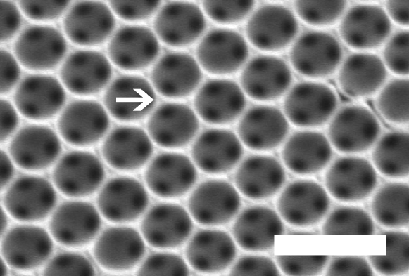
We have obtained the microscopic structure of our on-chip Si inverse opal crystal from high resolution scanning electron micrographs (SEM). From planar and cross-sectional SEM images we infer that our inverse opal is a fcc crystal. The size of the lattice parameter of the fcc-lattice is obtained from Fig. 1, which shows a top view of a {111} plane in the crystal. We find the lattice parameter to be a= 142720 nm, by measuring the lattice parameter along the three {} in-plane lattice directions, which allows us to correct for a 22∘ tilt of the sample.Wijnhoven01 From the lattice parameter and the number of terrace steps, we deduce a sample thickness of 7= 7a= 5.8 m.
We also observe from Fig. 1 that the interstices (indicated by arrows) in the {111} surface appear to be small. To describe the crystal with band structure calculations, we use a model of close packed air spheres (radius = a/) surrounded by spherical shells (radius ) connected by cylindrical windows (radius ) see Ref. Vos00, . From the almost filled interstices in Fig. 1, we estimate an outer shell radius of = 1.150.02. The radius of the air holes that interconnect the air spheres in the crystal are measured to be = 0.260.05 . This method results in a volume fraction of the solid material of about = 21.3 . Nevertheless, it should be realized that estimating volume fractions from SEM images can be problematic, as was found in in-situ x-ray experiments.Wijnhoven01
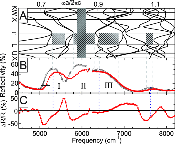
From the structural parameters obtained, we have calculated the photonic band structure by a plane-wave expansion method described in detail in Ref. Koenderinkthesis, . We have used a dielectric constant = 12.74 (at = 6535 cm-1) that was measured on a separately deposited reference sample.Kalkmanthesis The resulting photonic band structure calculation is plotted in Fig. 2(A). The open symbols in Fig. 2(B) represent a linear reflectivity spectrum of the sample. It is remarkable that the measured peaks correspond to the predicted stop gaps, since our model does not include freely adjustable parameters.
II.2 Ultrafast switching setup
Our setup consists of a regeneratively amplified Ti:Sapph laser (Spectra Physics Hurricane) which drives two optical parametric amplifiers (OPA, Topas). Both OPAs have a continuously tunable output frequency between 3850 and 21050 cm-1, with pulse durations of 150 fs and a pulse energy of at least 20 J. The independent tunability of our OPAs allows us to optimize the pump frequency, while scanning the probe frequency over a broad frequency range. The pump beam is incident at = 15∘, and has a much larger Gaussian focus of 133 m full width at half maximum (FWHM) than the probe, providing good lateral spatial homogeneity. The probe beam is incident at normal incidence = 0∘, and is focused to a Gaussian spot of 28 m FWHM at a small angular divergence NA= 0.02. Therefore, we ensure that only the central flat part of the pump focus is probed. The reflectivity was calibrated by referencing to a gold mirror. A versatile measurement scheme was developed to subtract the pump background from the probe signal, and to compensate for possible pulse-to-pulse variations in the output of our laser, see Ref. Euser06b, .
III RESULTS AND DISCUSSION
III.1 Linear reflectivity spectra
The linear reflectivity spectra in Fig. 2(B) demonstrates three stops band in the frequency range = 5000-7000 cm-1, similar to earlier work.Blanco00 ; Vos00 ; Vlasov01 ; Palacios02 We compare them to a calculated band structure diagram, and label the stop bands. Stop band I at frequency = 5320 cm-1 displays a maximum reflectivity R= 51 and is identified with the -L stop gap at frequency a/= 0.76 in the calculated bandstructure shown in Fig. 2(A). At = 5950 cm-1, we observe a stop band, labeled II, with maximum reflectivity R= 60. Stopband II corresponds to the stop gap at a/= 0.85 in Fig. 2(A). It is important to note that stop band II overlaps the frequency range of the predicted band gap that is centred around a/= 0.85. Stop band III at = 6500 cm-1 aligns with the stop gap at a/= 0.94. The frequency of the small peak at = 7616 cm-1 matches that of the stop band at a/= 1.08.
We have systematically reproduced our data on various positions on the sample. The peak reflectivity of all peaks varies by less than 10 with position. The variation is possibly due to variations in the density of lattice defects throughout the crystal. The center frequency of the stop bands, however, were found to be independent of position on the sample (within 1), which leads to the important conclusion that the crystal lattice is indeed the same everywhere in the sample.
The agreement between reflectivity peaks and theoretical stop gaps demonstrates that expected surface effects do not impede the ability of exploiting reflectivity measurements to probe bulk properties. We must note that, despite the apparent good agreement, a direct comparison between reflectivity data and band structure calculations is strictly speaking not allowed, since band structure calculations assume an infinitely extended crystal, and do not take into account surface effects. For instance, a large impedance mismatch of external modes and internal modes as a result of flat bands in the band structure can also lead to an increased reflectivity. A stop gap in the band structure calculations, however, should always result in an increased reflectivity, which is indeed the case here.
III.2 Switched reflectivity spectra
We have induced large and ultrafast reflectivity changes in our crystal by optically exciting free-carriers. The ultrafast response of the stop bands is acquired by measuring the reflectivity spectra at fixed probe delays. In experiments on the red part of the spectrum (6250 cm-1), the pump frequency was chosen to be = 6450 cm-1. In experiments on the blue edge (6250 cm), the pump frequency was reduced to = 5000 cm-1. The switched reflectivity spectra were measured in the same run and on the same spot on the sample as the linear data are shown as closed circles in Fig. 2(B). Due to dispersion in the probe path of the setup, there is a 500 fs variation of the delay time with frequency, we therefore measure the switched reflectivity at a fixed time delay of 1 ps. Figure 2(B) shows measurements of the switched and linear reflectivity in the range of second order Bragg diffraction of the sample at normal incidence.
The dispersion and propagation of light in the crystal is strongly modified by the switching. Consequently, we observe large variations in the reflectivity near the peaks in the region of second order Bragg diffraction. On the red edge of peak I, near = 5110 cm-1, the reflectivity strongly decreases, while on the blue edge, at = 5500 cm-1 we observe a strong increase in the reflectivity, indicative of a blue shift of the entire peak. Our crystals are therefore highly suitable to control the directional propagation of light.
The magnitude of the frequency shift of the peaks was obtained by measuring the frequency position of the red edge of stop band I, indicated by the black arrow in Fig. 2(B). The switching moves the edge towards higher frequencies, while the slope of the stop band edge remains unchanged. Only at the highest intensity used, induced absorption can slightly change the slope of the edge. However, the contribution of this effect to the measured shift is negligibly small.
The blue-shift of peak I is as large as 80 cm-1 or = 1.5. The same effect occurs on the red edge of peak II, near = 5800 cm-1, where the reflectivity decreases, and on the blue edge of peak III, near = 7000 cm-1, where the reflectivity increases. The blue edge of stop band III has blue-shifted by 50 cm-1 or = 0.7. Importantly, all stop bands have shifted towards higher frequency. We therefore conclude that switching has reduced the average refractive index of the crystal.
The shift of the stop bands is clearly evidenced by the dispersive features in the differential reflectivity of the sample that is plotted in Fig. 2(C). On the red edge of stop band I, at = 5110 cm-1, we observe a large decrease in the reflectivity by R/R= -54, while at = 5500 cm-1 we observe a strong increase in the reflectivity by R/R= 49. This distinct dispersive shape that is centered at around 5320 cm-1 is related to a large blue shift of stop band I; the observation of positive differential reflectivity indicates that the induced absorption remains small. Peak II and III are slightly broadened by disorder in the sample and thus appear as a single peak in the spectrum. On the red edge of the combined peak, at = 5800 cm-1 the differential reflectivity is R/R= -35, while at the blue edge of the peak, at = 7020 cm-1 the differential reflectivity amounts to R/R= +30; here the dispersive shape also has a strong positive component, which again signals low induced absorption. The strong dispersive shape that is centered around 6450 cm-1 is related to a large blue shift of the combined stop bands II and III. The strong dispersive curve that is centered around = 7600 cm-1 shows that the small peak at this frequency also shifts towards higher frequency.
The observed shift of stop band II towards higher frequency is particularly interesting, as this stop band is part of the predicted band gap for inverse opals. We have thus demonstrated switching of a 3D photonic band gap, which has not been reported before. The switching process is expected to lead to ultrafast changes of the density of states inside the crystal.Johnson02
Remarkably, we observe that both the low and high frequency edge of the stop bands have shifted. This indicates the absence of separate dielectric and air bands in the range of second order Bragg diffraction in inverse opals, which is consistent with predictions based on quasi-static band structure calculations by Ref. Johnson02, . From our comparison we find a refractive index change of n’/n’ 2 and a carrier density of = 2.1 cm-3. The corresponding plasma frequency is = 3623 cm-1, which is equal to 0.72. We conclude that excellent switching conditions indeed appear if the plasma frequency remains smaller than the probe frequency as predicted in Section I.
III.3 Switching time traces
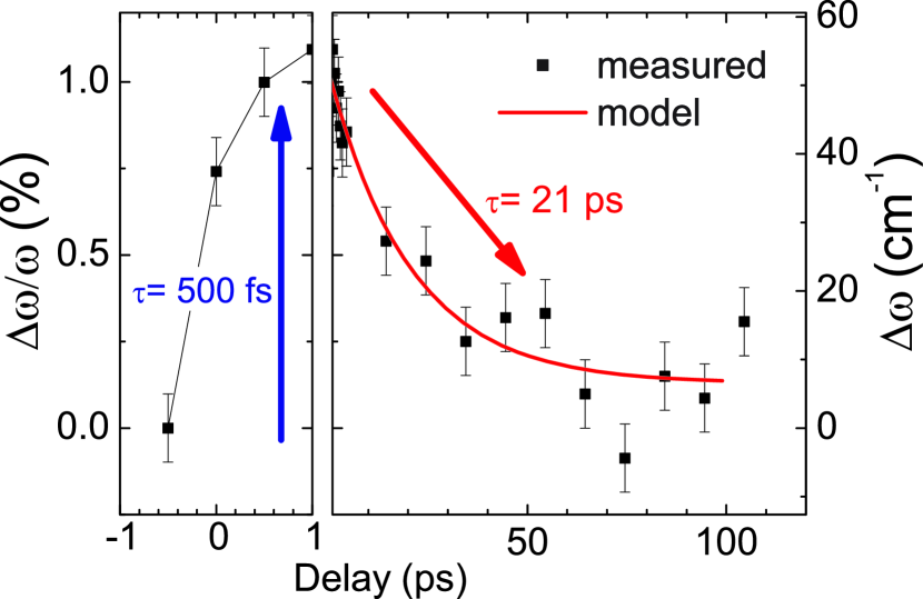
The large and ultrafast shift of the stop band with time is studied in detail in Fig. 3. We have measured the frequency position of the red edge of the stop band at = 5045 cm-1, at a large range of delay times after excitation. From each spectrum, the frequency position of the low frequency edge was determined at R= 15 (indicated by the arrow in Fig. 2(B)). The relative frequency shift is plotted versus probe delay in Fig. 3. We observe a large and ultrafast shift of the stop band edge from 0 to = 1.1 with an exponential growth time of = 500 fs, limited by the pulse duration of our pump pulses.
The effect subsequently decreases exponentially with a decay time of = 214 ps (least squares fit) to a small residual shift = 0.1. The decay times are much faster than carrier relaxation times in bulk Si, since our photonic crystals are made of poly crystalline silicon, whose lattice defects and grain boundaries act as efficient carrier recombination traps.Yu96 The short relaxation time is in good agreement with the typical carrier relaxation time of 18 ps that we found in poly-Si woodpile crystals.Euser06b The relatively fast decay time implies that switching could potentially be repeated at GHz rates, which is relevant to possible future switching and modulation applications.
III.4 Induced probe absorption
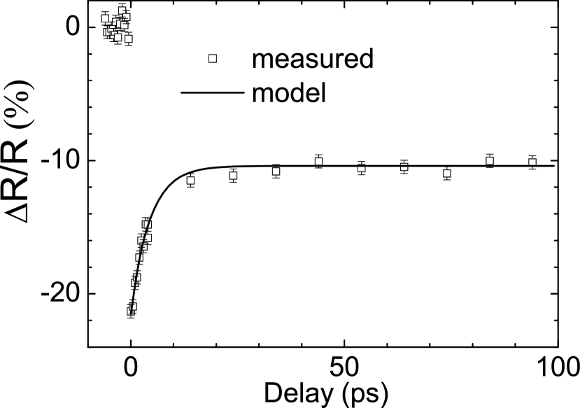
Besides a frequency shift which is related to a change in the real part of the refractive index, we observe a decrease of the reflectivity peak, which is associated with an increase in . The induced absorption manifests itself in a reduction of the reflectivity maximum after excitation. We therefore plot in Fig. 4 the relative decrease in reflectivity maximum of stop band II at frequency = 5882 cm-1 as a function of delay time. The data were obtained in the same run as the experiment shown in Fig. 3. The maximum decrease in reflectivity of the stop band directly after excitation, is R/R -21. Note that this decrease is not only due to absorption but also to a shift. In Ref. Euser06b, we have related a reduction in peak reflectivity of woodpile samples to the induced absorption through exact model method calculations. Due to difficulties in calculating the reflectance using a complex dielectric function in inverse opals, we estimate the induced absorption by comparing the observed R/R= -21 to the calculated decrease in Si woodpile crystals. For woodpile photonic crystals theory that can handle a complex dielectric function is available.Euser06b From this comparison we estimate an upper bound to the induced absorption in the Si backbone to be . We use the Si volume fraction = 21.3, obtained in II.1, to describe our crystal as an effective medium consisting of Si and air. In more advanced studies, one could also take the spatial distribution of the probe light in the crystal into account.Tan04 Since only a fraction of our crystal absorbs light, we can estimate the resulting probe absorption length in our switched inverse opal to be = 6.3 m. The obtained value is larger than the thickness of the sample L= 7= 5.8 m. We conclude that for refractive index changes larger than 2, will increase further, and consequently the crystal may lose its transparency. Likewise, in applications in which much smaller changes in the refractive index suffice, the induced absorption will become negligible small.
Figure 4 also shows how the reflectivity change evolves in time after the initial decrease to . The effect decays exponentially to with a decay time of 4 1 ps, followed by a much slower decay with about ns decay times. The fast relaxation process is likely related to the fast recombination of carriers in the poly-Si backbone of the crystal that was discussed in the previous Section. It is presently unclear why the induced absorption decays about five times faster than the induced stop band shift shown in Fig. 2(B), which was obtained from the same set of spectra. The subsequent, much slower recombination process at ns times is attributed to recombination of excited carriers in the underlaying Si-wafer substrate. In bulk Si at the carrier densities in our experiment (1019 cm-3), carrier recombination is dominated by Auger effects with recombination times of the order of 10 ns.Dziewior77 Any change in the substrate is likely to change the magnitude of the reflectivity of the whole sample, while it should not affect the frequency positions of the stop bands in Fig. 2, which are related to changes in the backbone of the photonic crystal only. Indeed, we find that the stop band shift in Fig. 3 decays rapidly within 100 ps, to a small offset of a few wavenumbers. Meanwhile, a large part of the reflectivity decrease in Fig. 4 is still present after 100 ps, and continues to decay on ns timescales, consistent with the slow recombination of carriers in the wafer substrate.
In our experiments we have used two-photon absorption at long pump wavelengths combined with a large pump focus to maximize the spatial homogeneity of the switched crystals. The pump fluence in our experiments was typically 25 pJ per unit cell area per pulse. In applications with small active areas, typical for 2D and 3D cavities, spatial homogeneity is not an important issue and thus low pump fluences suffice. Furthermore, the pump fluence can be further reduced by choosing the pump wavelength in the linear absorption range.Euser05
IV CONCLUSIONS
In this Paper, we have studied all-optical ultrafast switching of a high-quality 3D Si inverse opal photonic band gap crystal in the frequency range of second order Bragg diffraction. A spatially homogeneous free-carrier plasma was optically excited in the crystal by a two-photon process. We show that for Si inverse opals, good experimental conditions are found for free-carrier plasma frequencies around = 0.3-0.7; large changes in the refractive index can be achieved, while the crystal remains transparent after the switching. We find good agreement between the stop bands in the linear reflectivity spectra and calculated stop gaps in the frequency range of the band gap. Switching effects are studied as a function of time delay between pump and probe pulses. Large ultrafast variations in reflectivity are observed in the range of second order Bragg diffraction. During the switching process, all spectral features in the observed stop bands, shift towards higher frequencies by as much as = 1.5 within a few hundred fs, indicating the absence of separate dielectric and air bands in our crystal. From a comparison to quasi-static band structure calculations of Ref. Johnson02, we infer a large refractive index change of about 2. The deduced refractive index change is predicted to strongly modify the density of states inside the crystal.Johnson02 We have observed a relatively fast decay time of 21 ps, which implies that switching could potentially be repeated at a GHz rates, which is relevant to possible future switching and modulation applications.
ACKNOWLEDGMENTS
We thank Cock Harteveld and Rob Kemper for technical support, Martin Wegener, Ad Lagendijk, Dimitry Mazurenko, and Patrick Johnson for discussions. This work was also reported on arXiv.org/abs/0705.4250. This work is part of the research program of the ”Stichting voor Fundamenteel Onderzoek der Materie” (FOM), which is supported by the ”Nederlandse Organisatie voor Wetenschappelijk Onderzoek” (NWO). This work was also supported in part by the ACS Petroleum Research Fund, the US NSF (CTS-0332484), and the US DOE (DE-FG02-06ER46348). We also utilized the Nano Fabrication Center and the Characterization Facility at the University of Minnesota which receive partial support from US NSF through the NNIN program. DJN acknowledges support from the Alexander von Humboldt Foundation.
References
- (1) ’Photonic Crystals and Light Localization in the 21st Century’, Ed. C. M. Soukoulis (Kluwer, Dordrecht, 2001).
- (2) E. Yablonovitch, Phys. Rev. Lett. 58, 2059 (1987).
- (3) P. Lodahl, A. F. van Driel, I. Nikolaev, A. Irman, K. Overgaag, D. Vanmaekelbergh, and W. L. Vos, Nature 430, 654 (2004).
- (4) S. W. Leonard, H. M. van Driel, J. Schilling, and R. B. Wehrspohn, Phys. Rev. B 66, 161102 (2002).
- (5) H. Nakamura, Y. Sugimoto, K. Kanamoto, N. Ikeda, Y. Tanaka, Y. Nakamura, S. Ohkouchi, Y. Watanabe, K. Inoue, H. Ishikawa, and K. Asakawa, Opt. Express 12, 6606 (2004).
- (6) P. M. Johnson, A. F. Koenderink, and W. L. Vos, Phys. Rev. B 66, 081102(R) (2002).
- (7) M. F. Yanik and S. Fan, Phys. Rev. Lett. 92, 083901 (2004).
- (8) K. Sokolowski-Tinten and D. von der Linde, Phys. Rev. B 61, 2643 (2000).
- (9) T. G. Euser and W. L. Vos, J. Appl. Phys. 97, 043102 (2005).
- (10) D. A. Mazurenko, R. Kerst, J. I. Dijkhuis, A. V. Akimov, V. G. Golubev, D. A. Kurdyukov, A. B. Pevtsov, and A. V. Sel’Kin, Phys. Rev. Lett. 91, 213903 (2003).
- (11) C. Becker, S. Linden, G. von Freymann, M. Wegener, N. Tétreault, E. Vekris, V. Kitaev, and G. A. Ozin, Appl. Phys. Lett. 87, 091111 (2005).
- (12) J. E. G. J. Wijnhoven and W. L. Vos, Science 281, 802 (1998).
- (13) A. Blanco, E. Chomski, S. Grabtchak, M. Ibisate, S. John, S. W. Leonard, C. López, F. Meseguer, H. Míguez, J. P. Mondia, G. A. Ozin, O. Toader, and H. M. van Driel, Nature 405, 437 (2000).
- (14) W. L. Vos and H. M. van Driel, Phys. Lett. A 272, 101 (2000).
- (15) Y. A. Vlasov, X- Z. Bo, J. C. Sturm, and D. J. Norris, Nature 414, 289 (2001).
- (16) E. Palacios-Lidon, A. Blanco, M. Ibisate, F. Meseguer, and C. López, Appl. Phys. Lett. 81, 4925 (2002).
- (17) T. G. Euser, A. J. Molenaar, J. G. Fleming, B. Gralak, A. Polman, and W. L. Vos, http://arxiv.org/abs/physics/0603045 (2006).
- (18) K. Busch and S. John, Phys. Rev. E 58, 3896 (1998).
- (19) A. F. Koenderink, Emission and transport of Light in Photonic Crystals, ISBN 90-9016903-2, University of Amsterdam (2003).
- (20) H. S. Sözüer, J. W. Haus, and R. Inguva, Phys. Rev. B 45, 13962 (1992).
- (21) K. M. Ho, C. T. Chan, and C. M. Soukoulis, Phys. Rev. Lett. 65, 3152 (1990).
- (22) P. Jiang, J. F. Bertone, K. S. Hwang, and V. L. Colvin, Chem. Mater. 11, 2132 (1999).
- (23) J. Kalkman, Controlled spontaneous emission in erbium-doped microphotonic materials, ISBN 90-363-0295-2, University of Utrecht, (2005).
- (24) J. Kalkman, E. de Bres, A. Polman, Y. Jun, D. J. Norris, D. C. t Hart, J. P. Hoogenboom, and A. van Blaaderen, J. Appl. Phys. 95, 2297 (2004).
- (25) J. E. G. J. Wijnhoven, L. Bechger, and W. L. Vos, Chem. Mater. 13, 4486 (2001).
- (26) P. Y. Yu and M. Cardona, Fundamentals of Semiconductors, Springer-Verlag, Berlin, (1996).
- (27) H. W. Tan, H. M. van Driel, S. L. Schweizer, R. B. Wehrspohn, and U. Gsele, Phys. Rev. B 70, 205110 (2004).
- (28) J. Dziewior and W. Schmid, Appl. Phys. Lett. 31, 346 (1977).