Local tunneling spectroscopy of the electron-doped cuprate Sm1.85Ce0.15CuO4
Abstract
We present local tunneling spectroscopy in the optimally electron-doped cuprate Sm2-xCexCuO4 x=0.15. A clear signature of the superconducting gap is observed with an amplitude ranging from place to place and from sample to sample ( 3.5-6meV). Another spectroscopic feature is simultaneously observed at high energy above 50meV. Its energy scale and temperature evolution is found to be compatible with previous photoemission and optical experiments. If interpreted as the signature of antiferromagnetic order in the samples, these results could suggest the coexistence on the local scale of antiferromagnetism and superconductivity on the electron-doped side of cuprate superconductors.
pacs:
74.25.Gz, 74.72.Jt, 75.30.Fv, 75.40.-sDue to strong correlations, doping a Mott insulator yields a number of fascinating properties in a great number of materials. Among these, understanding the properties of cuprates remains one of the greatest challenges in condensed matter physics. In recent years, an important effort has been made to understand the interplay between the antiferromagnetic (AF) and the superconducting orders. A close relation between these two is undeniably present on the electron doped side of the phase diagram since both orders overlap in a a narrow doping range. This observation was first reported by angle resolved photoemission (ARPES) when revealing the presence of a large energy gap on parts of the Fermi surface ArmitageNCCO in superconducting samples. The particular symmetry of this large energy gap, which happens at the interception between the nominal Fermi surface and the antiferromagnetic Brillouin zone, has led to its interpretation as the signature of AF order in the sample. The characteristic temperature T’ below which this large energy gap opens has since been mapped out over the phase diagram by infrared spectroscopy Onose ; Zimmers , revealing its presence up to x=0.17 in superconducting PCCO samples. However, neither ARPES nor infrared spectroscopy are able, in principle, to differentiate if this large energy gap is due to long range AF order or AF fluctuations. These technics can only estimate at best the minimum fluctuation length and time scales involved. A recent inelastic neutron diffraction measurement Greven has resolved this issue by showing that in superconducting samples, the antiferromagnetic correlation length does not diverge but saturates at low temperatures. This suggests that only AF fluctuations are present with a characteristic length scale of 200Å in optimally doped samples. An important challenge is now to see whether both orders do coexist on a local scale.
To answer this question, we report a first set of local tunneling spectroscopy measurements in STM geometry on the electron-doped cuprate Sm1.85Ce0.15CuO4 (SCCO) on larger energy scales. The tunneling conductance spectra show simultaneously the superconducting gap at low energies and a high energy feature at same spatial positions. The attribution of this high energy feature to the presence of local AF order suggests that, in electron-doped cuprates, antiferromagnetism and superconductivity coexist locally at optimal doping. In addition to these various energy scales, our measurements have revealed no changes in the superconducting gap magnitude within a 330Å map but show large variations of this gap (up to 70%) between distant points within a same sample and between two different optimally doped samples. These large variations could be explained by modulation of the cerium and oxygen content within the samples. This observation is different from previous scanning tunneling microscopy (STM) measurements in the hole-doped cuprate Bi-2212 which show local inhomogeneities in the superconducting gap on the nanoscale Cren ; Davis .
Local electronic properties are probed by scanning tunneling microscopy/spectroscopy (STM/STS), where the tunneling current is measured between an atomically sharp tip and a sample as a function of the bias voltage. Images of the surface can be made by scanning the tip (topographic mode) or at a given point (spectroscopic mode). The tunneling junctions were achieved by approaching mechanically cut Pt/Ir tips (whose density of states (DOS) near the Fermi level is roughly constant) to the c-axis oriented surface of the crystals. This configuration is believed to be most sensitive to the DOS of the planes of SCCO. The differential conductance measured, , is proportional to the sample local DOS convoluted with the Fermi function (at the energy + eV).
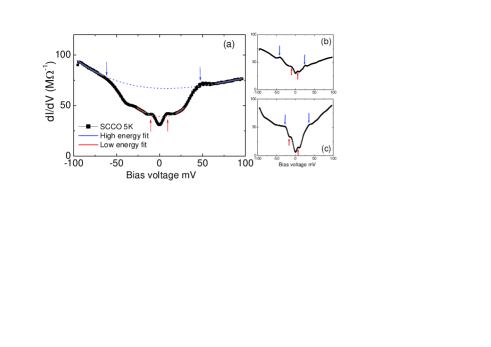
(b) and (c) Raw spectra on the same sample but at distant positions. The superconducting gap is always centered around zero bias as expected, however we observe that the high energy feature can be shifted to negative (panel (b)) or to positive bias (panel (c)) depending on the location.
(b) High energy feature isolated by dividing out the high energy background (blue fit figure 1). The high energy feature magnitude is identifiable by the blue arrows.
Single crystals of Sm2-xCexCuO4 were grown by flux method. Samples were typically a few mm along a and b axis and a few hundred microns along c axis. Samples were annealed at 925℃ under reduced oxygen environment for 3 to 5 days. Ce concentrations were determined by WDX. Superconducting transition temperature were determined by DC susceptibility. The two samples presented here are SCCO with cerium concentrations x=0.1450.005 with an onset =20K and SCCO x=0.1550.005 with an onset =17.5K. These concentrations are just an indications of the carrier density in the samples. Indeed the sample carrier density can also slightly change due to various oxygen reduction treatments. These different treatments could, for instance, explain the small differences in the measured critical temperatures Higgins even though both samples are near optimally doped in cerium. These materials were chosen since they present the advantage of being cleavable compared to other electron-doped cuprates such as Nd2-xCexCuO4 (NCCO) and Pr2-xCexCuO4 (PCCO).
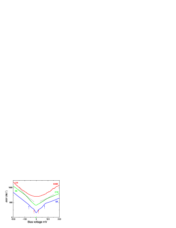
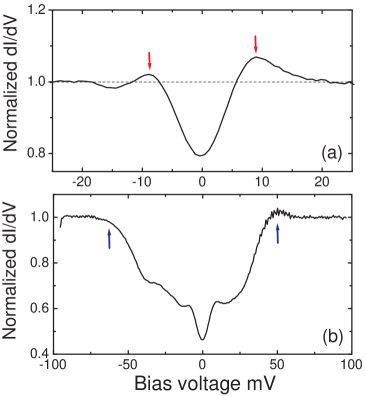
In figure 1 we present a typical spectrum obtained at 5K. One can distinguish a low energy feature (see lower red arrows). The shape and the temperature dependence of this features allow us to identify it with the superconducting gap. The shape of the feature can be isolated in figure 2 (a) when dividing out the ‘U’ shaped background (red fit figure 1 named ‘low energy fit’). As discussed further, this background choice is the best representation of the spectra above . By isolating the low energy feature in figure 2 (a), one can then notice weak coherence peaks in the spectrum. These peaks are incompatible with the low energy pseudogap measured by tunnel junction measurements Alff ; DaganPG but compatible with the signature of the superconducting gap. The zero bias conductance (ZBC) value of 80% is slightly higher than other well studied cuprates such as YBCO where the ZBC is generally found to be around 50%. Using this spectrum one finds the gap value from peak to peak to be =18meV. In a BCS picture this corresponds to a gap of =12meV. Using this extraction method, tunneling spectra measurements performed at various distant points on a same sample and on two different optimally doped samples show a superconducting gap ranging from 7meV to 12meV. These variations could be explained by inhomogeneities on large scales in the oxygen content arising in the reduction process and/or variation of cerium concentration on the micron scale. Using these gap values we find a ratio / varying from 4 to 7. Other spectroscopic techniques find this ratio to be 4.4 from Raman Blumberg in NCCO, 2.3 from photoemission in PLCCO MatsuiSupra , 5 from optical conductivity of optimally doped PCCO ZimmersSupra and 3.4 in NCCO and PLCCO from point contact tunneling spectroscopy Shan . All of these ratios are on the lower limit of the one we find in SCCO. Figure 3 presents the temperature dependence from 5K to 300K on a second optimally doped sample. When raising the temperature through the superconducting transition from 5K to 27K, one observes that the low energy feature vanishes. All of the arguments described above allow us to identify this low energy feature with the superconducting gap.
We now discuss the high energy part of the spectra. Similar to the analysis used to isolate the superconducting gap, we have adjusted the conductance background above and below the high energy feature. This background fit presented in blue in figure 1 is divided out to give figure 2 (b). We have chosen the simplest background line in order to isolate the characteristic energy scale of the high energy feature. Note that such a ’U’ shaped background is also observed in many other superconducting cuprates such as YBCO. The magnitude of the high energy feature is identified to be ’=120meV (see blue arrows presented in figure 1 and figure 2 (b)). This value is comparable in magnitude with the large energy pseudogap measured by ARPES ArmitageNCCO ; ArmitageSCCO and optical spectroscopy in NCCO Onose , PCCO Zimmers and SCCO ArmitageSCCO . However, further quantitative comparison is hard to pursue since the estimate of the large energy pseudogap maggnitude clearly depends on the spectroscopy technique used. Indeed, a recent study on a unique underdoped SCCO sample ArmitageSCCO has shown that the estimate of the large energy pseudogap varies from 200meV to 300meV when measuring by photoemission or optical conductivity. The most interesting and controversial aspect of this spectrum is the observation of the superconducting gap and large energy pseudogap at the same local measurement points. The resolution of the tip was evaluated to be 10 Å. The vast majority of data recorded using various samples showed both gaps in each spectrum. If the high energy feature is identified to be the signature of an antiferromagnetic order in the sample, this would then imply that both superconductivity and antiferromagnetism could coexist locally.
The spectra shown in figure 1(a) presents the advantage of
being symmetric with respect to the zero-bias voltage. This symmetry
is not always present in the data. Indeed, in many spectra the high
energy features were shifted to one or the other sides of the
zero-bias voltage (see figure 1 (b) and (c)). This
asymmetry could be understood using the following arguments:
- The
measured tunnelling spectra result from averaging over the entire
Fermi surface. Contrary to tunneling in simple metal, in complex
materials such as SCCO, this averaging could be weighted in
preferential directions of -space due to particular geometry
between the tip and the surface Footnote1 . If this tunneling
configuration changes while probing spatially distant points of a
sample, this should be followed by a variation in the weighting
factors.
- In the particular case of SCCO, these variations could
generate important modifications of the tunneling spectra. Indeed,
when ordered antiferromagnetically, SCCO band structure is found to
be a two-band system near the Fermi energy ArmitageNCCO ; ArmitageSCCO (see Figure 4 (b)). By definition, the gap
between both bands will appear to be centered with respect to the
Fermi energy if the tunneling current is most sensitive to the
nesting points (hot-spots). However, this gap will appear to be
off-centered and larger if the current is most sensitive to the
antinodal regions (,0) or (0,) (see blue arrow figure
4b) or the nodal region (/2,/2) direction (see
dashed blue arrow, figure 4b).
We now turn to the temperature dependence of this high energy feature. Figure 3 shows the SCCO spectra of a different optimally doped sample x=0.155 (having a slightly lower than the sample discussed previously in figure 1 and 2) at three different temperatures, 5K, 27K and 300K. Considering temperature drifts, the three spectra were taken in the same local region and represent typical results obtained when raising the temperature. At low temperatures one can again identify two energy scales represented by the red and blue arrows. When passing above the superconducting transition temperature, the superconducting gap closes but the high energy feature remains. However, when raising the temperature to room temperature, we observe the closing of this energy gap, only leaving the overall ‘U’ shaped line, similar to the background fit used previously. Since the closing of the large energy pseudogap has been shown to be smooth Zimmers , it is difficult to identify the characteristic temperature T’ above which this feature disappears in the conductance spectra. However, optical measurements of NCCO and PCCO were able to establish the relation /=16 between the pseudogap energy ’ and the gap characteristic opening temperature T’. Using this relation and the value ’=90meV from figure 3, one finds T’=130K for this sample. This simple estimate of T’ explains why one observes the high energy gap at 5K and 27K but not at 300K.
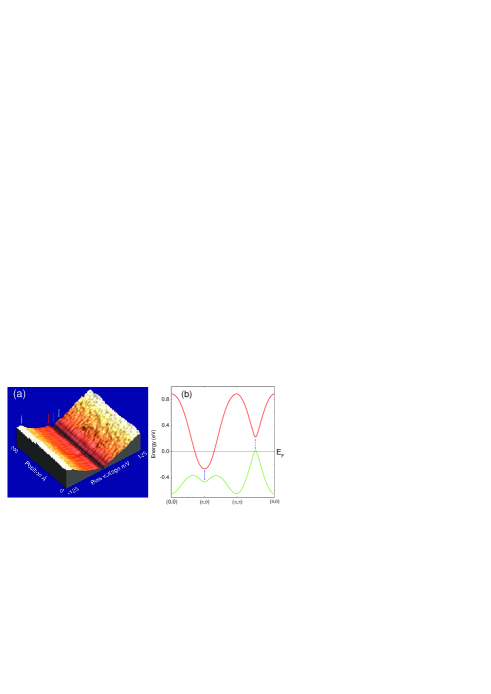
Figure 4 (a) presents the tunnel spectra taken along a 200Å line chosen from a topographic/spectrographic measurement of a 330Å2 square. The superconducting gap is observed around zero bias voltage (see red arrows). The high energy feature is clearly seen on the negative bias voltage side and is only suggested on the positive bias voltage side (see blue arrows) Footnote2 . In this scenario, the high energy feature is found to range from -100meV to +30meV making it comparable in energy (but shifted towards negative bias) with respect to the high energy feature presented in figure 1(a) (both spectra were measured in regions close by). Moreover this image shows that both the high and low energy features are very stable in amplitude throughout nanometer distances. The homogeneity of the superconducting gap magnitude following a 35nm line scan was previously reported in NCCO Kashiwaya . This suggests that the DOS map fluctuation observed in hole-doped cuprates Cren ; Davis is not observed in electron-doped cuprates on the same scale. The variation in the superconducting gap mentioned previously at various distant points on the surface can be explained by slight inhomogeneities in the oxygen content arising in the reduction process.
We have reported the normal state and superconducting state local tunneling spectra of SCCO. On a large scale, the superconducting gap is observed to range from 3.5meV to 6meV, the ratio / thus varying from 4 to 7. At low temperatures a large energy feature in the tunneling spectra is observed. This one remains above but disappears at higher temperatures. On the nanometer scale the amplitudes of the superconducting gap and the high energy feature are found not to vary with position. The high energy feature could be the signature of the large energy pseudogap observed by photoemission and optical spectroscopy (interpreted as the signature of AF order). In this case these results would suggest the coexistence on a local scale of antiferromagnetism and superconductivity. Further measurements need to be performed to confirm this interpretation.
This work was supported by NSF grants DMR-0352735, DMR-0303112 and DMR-0645461. A.Z. acknowledges Fellowship support from the ICAM International Materials Institute.
References
- (1) N.P. Armitage et al., Phys. Rev. Lett. 88, 257001 (2002).
- (2) Y. Onose et al., Phys. Rev. B 69, 024504 (2004).
- (3) A. Zimmers et al., Europhys. Lett., 70 (2), pp. 225-231 (2005).
- (4) E.M. Motoyama , cond-mat/0609386 (2006).
- (5) T. Cren, D. Roditchev, W. Sacks et al., Phys. Rev. Lett. 84, 147 150 (2000). T. Cren et al., Europhys. Lett. 54, 84-90 (2001); C. Howald, P. Fournier, and A. Kapitulnik, Phys. Rev. B 64, 100504 (2001); S.H. Pan et al., Nature 213, 282 (2001).
- (6) K. McElroy et al., Science 309, 1048 (2005).
- (7) J. S. Higgins et al., Phys. Rev. B 73, 104510 (2006).
- (8) L. Alff ., Nature, 422, p698-701 (2003).
- (9) Y. Dagan, M. M. Qazilbash, and R. L. Greene, Phys. Rev. Lett. 94, 187003 (2005).
- (10) G. Blumberg et al., Phys. Rev. Lett. 88, 107002 (2002).
- (11) H. Matsui et al., Phys. Rev. Lett. 95, 017003 (2005).
- (12) A. Zimmers et al., Physical Review B, 70, 132502 (2004); C. C. Homes et al., Phys. Rev. B 74, 214515 (2006).
- (13) L. Shan et al., cond-mat/0703256 (2007).
- (14) N.P. Armitage et al., cond-mat/0612419 (2006).
- (15) A study of all possible reasons leading to such asymmetries will be pursued in the future.
- (16) I. Horcas, R. Fernandez, J.M. Gomez-Rodriguez, J. Colchero, J. Gomez-Herrero and A. M. Baro, Rev. Sci. Instrum. 78, 013705 (2007).
- (17) Figure curtesy of A. J. Millis.
- (18) In some particular line scans, a probable Coulomb blockage is occasionally observed at higher energy but changes with position making it unrelated to the other spectroscopic features mentioned.
- (19) S. Kashiwaya et al., Phys. Rev. B 57, 8680 (1998).