Mapping electron delocalization by charge transport spectroscopy in an artificial molecule
Abstract
In this letter we present an experimental realization of the quantum mechanics textbook example of two interacting electronic quantum states that hybridize forming a molecular state. In our particular realization, the quantum states themselves are fabricated as quantum dots in a molecule, a carbon nanotube. For sufficient quantum-mechanical interaction (tunnel coupling) between the two quantum states, the molecular wavefunction is a superposition of the two isolated (dot) wavefunctions. As a result, the electron becomes delocalized and a covalent bond forms. In this work, we show that electrical transport can be used as a sensitive probe to measure the relative weight of the two components in the superposition state as a function of the gate-voltages. For the field of carbon nanotube double quantum dots, the findings represent an additional step towards the engineering of quantum states.
pacs:
73.63.-b, 73.23.-b, 03.67.-aIn the quantum world particles such as electrons behave as extended objects with the character of a wave. The combination of wave-like behaviour on the one hand and interactions on the other hand leads to ‘localized’ electron waves, also called quantum states. When two quantum states overlap, quantum interference results in a superposition state with new qualities. In particular, a molecular bond may emerge from the constructive interference of the quantum states. Engineered double quantum dots provide an experimental platform enabling one to control this prototype of molecular formation Livermore ; Blick ; Hatano ; Fasth ; dicarlo ; Holleitner ; pioro . In this letter, the molecular states are realized in a double quantum dot device gate-defined in a single-walled carbon nanotube (SWCNT) Mason ; sapmaz ; graebermol . We show that, by analyzing the electrical conductance through the device, it is actually possible to map the electron delocalization of the covalent chemical bond formed between the two quantum dots.
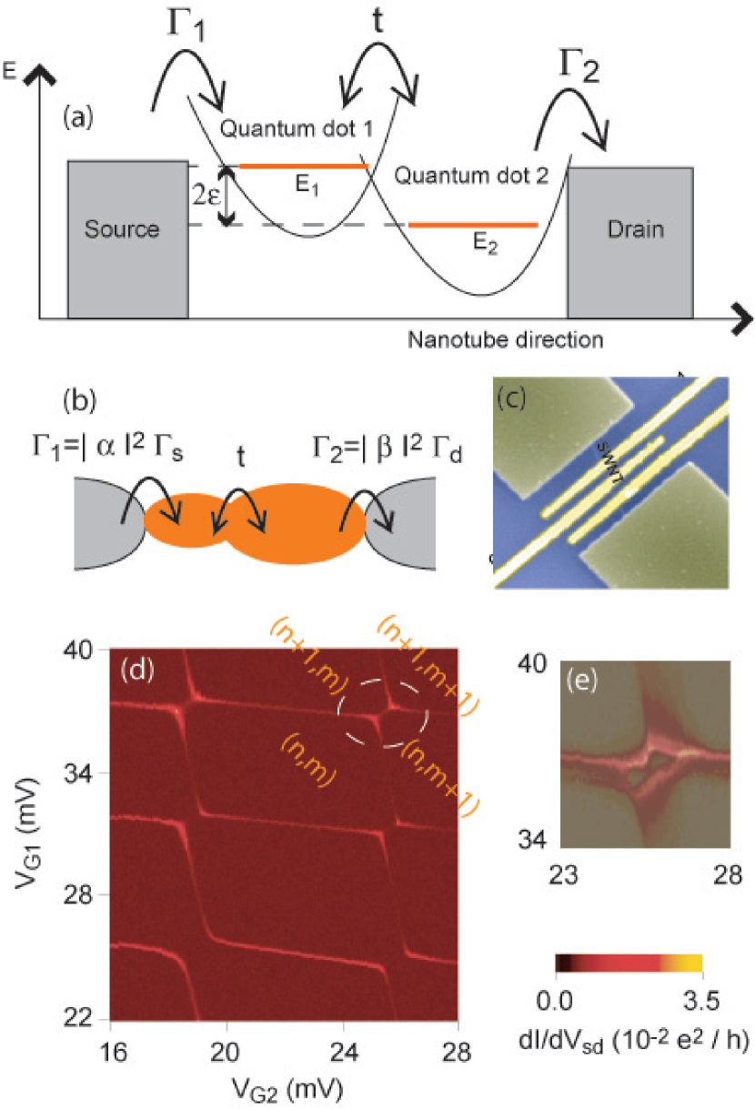
In Fig. 1(a-c) we show the experimental realization of our carbon nanotube double quantum dot device. A scanning electron micrograph of such a device, showing source and drain contacts and three top-gate electrodes in between can be seen in Fig. 1(c). The three top-gates can be used to adjust the electrostatic potential landscape within the nanotube as depicted in Fig. 1(a), yielding the double quantum dot structure. Using the outer two gate electrodes the difference of the level energies in the left and right dot, the detuning can be adjusted as well. Transport takes place through a molecular state as indicated in Fig. 1(b), provided the detuning is not much larger than the tunnel coupling , which in turn is proportional to the overlap of the dot wavefunctions. One can say that the detuning determines the degree of localization of the electron on the double quantum dot. Only for the probability of finding the electron on the left or the right dot will be comparable, for the electron will mainly be localized on one of the two dots.
In order to be more quantitative, we introduce a toy model of molecular formation which is capable of describing all basic features of our experiment. Our system consists of a left and a right quantum dot and a single electron, which can be put into the dots. Left and right dot are indexed by 1 and 2 , respectively. We neglect spin and consider only a single level per dot. The two levels of the two dots are tunnel-coupled, characterized by the coupling energy , which we take as a real parameter. In the basis of the single dot wavefunctions the system is described by the following Hamiltonian:
| (1) |
For the eigenvalues one obtains the energy of the bonding (+) and the anti-bonding (-) orbital: , where we have defined and the detuning , giving half the distance in energy between the unperturbed energies and . If there is no or only little interaction () between the two dots, the electron will reside in either the left or the right dot in an unperturbed eigenstate or , respectively. For stronger coupling , however, the electron becomes delocalized. In general, the eigenstates are then formed from a superposition
| (2) |
The probabilities of finding the delocalized electron on either the left dot or the right dot are given by and , respectively, with . The coefficients and depend on the detuning ; the probability of finding the electron on the left dot being given by:
| (3) |
Via the metallic source and drain electrodes, which are fabricated to the carbon nanotube by nano-lithography (see Fig. 1(c), one can pass an electrical current through the device. This current will be proportional to the joint probabilities of charge transfer between the source and the quantum state in quantum dot (facing the source electrode) and between the drain and the quantum state in dot (facing the drain electrode), exactly like in a single quantum dot. The probabilities are commonly referred to as charge transfer rate and , for source and drain electrode, respectively. In the case of a double quantum dot, when transport happens through a molecular wave function, one has to weight this transfer rate with the probability of the shared electron to be on the left or right dot ( and ), respectively. The transfer rates are then given by and and thus directly reflect the molecular wavefunction. As was shown in Ref. graebermol , the maximum linear differential conductance for sequential tunneling through the molecular level can be expressed as
| (4) |
where
| (5) |
Equation 4 is valid if spin-degeneracy is lifted. Otherwise there is a slight modification, which in linear transport only adds a correction factor and does not affect the following analysis Coish-Loss . Combining Eq. 3-5 yields as a function . When comparing this dependence with the experiment, the following three fitting parameters can in principle be extracted: (actually ), and . In practice, however, an accurate coordinate transfer from gate-voltages to and needs to be performed prior to this analysis, which also include additional fitting parameters in the form of various capacitors Coish-Loss . Here, we illustrate in the following that this procedure works and can yield sensible results.
Single-walled carbon nanotubes (SWNT) were grown by means of a chemical vapor deposition (CVD) hydrogen-methane based process 1998-Kong ; Comment-CVD on a degenerately doped silicon substrate, and located with a scanning-electron microscope (SEM). The three 100 nm wide SiO2/Ti/Pd top-gate electrodes and the Pd/Al source and drain electrodes were defined by electron beam lithography and physical vapor deposition graebermol . Electrical transport measurements using standard lock-in techniques were performed in a He3/He4 dilution refrigerator at an electronic temperature of 50 mK.
Figure 1(d) shows the differential conductance through the device at 50 mK in a colorscale representation. The bright (high-conductive) lines define the charge-stability map of a double quantum dot, often referred to as honeycomb pattern VanderWiel . Within each cell the number (n,m) of electrons residing on the two dots is constant. Increasing the voltage applied to the left (right) gate () successively fills electrons into the left (right) dot, whereas decreasing the gate voltages pushes electrons out of the dots. A situation, where n electrons are on the left dot and m electrons on the right one, is denoted by (n,m). The curvature of the high-conductive ridges indicates the formation of molecular electronic eigenstates of the system, induced by a sufficiently large tunnel coupling. In the following we will focus on the ridges separating the (n,m), (n,m+1), (n+1,m), (n+1,m+1) charge stability regions, marked by a dashed ellipse.
Next, the given gate voltages need to be transformed into the chemical potential of either quantum dot. From Fig. 1(d) it is apparent that neither the vertical nor the horizontal boundaries of the honeycomb cells run perfectly parallel to the gate voltage axis. This is due to a mutual capacitance between the two dots, which is small in carbon nanotube double dots as compared to other planar GaAs heterojunction devices, but still not negligible for the following analysis. Within an electrostatic model VanderWiel ; Bruder , the relations between gate voltages and chemical potential of the dots (including a constant offset) are given by:
| (6) |
where denotes the total capacitance of dot 1(2), with the capacitance of top-gate 1(2) and that of source and drain electrode, respectively. From measurements of the double dot stability map at finite bias (see Fig. 1(e)), the dimensions of the honeycomb cells, and the slope of the honeycomb boundaries, it is possible to evaluate all capacitances of the device graebermol ; Coish-Loss . Since these capacitances may vary for large differences in gate voltage, it is important to evaluate them for each triple point region of interest individually. For the triple point region marked by a dashed circle in Fig. 1(d), we obtain aF, aF, aF, aF, and aF.
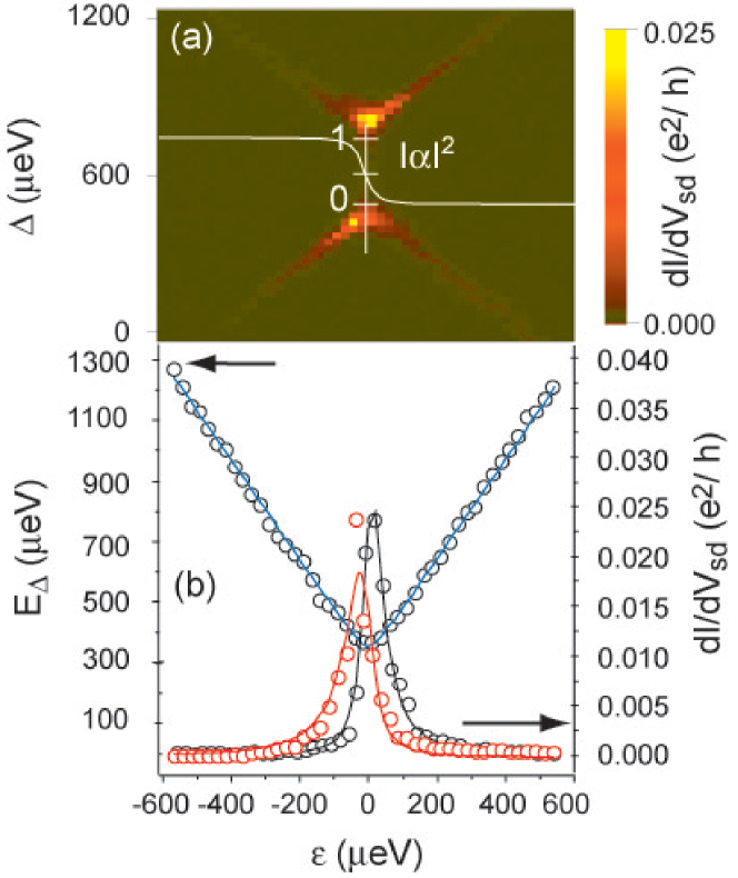
Figure 2(a) shows a colorscale plot the differential conductance of the above region versus and . The bottom high-conductive wing corresponds to the situation when the bonding state is degenerate with the charge state . Correspondingly, in the upper high-conductive wing, and are degenerate. The spacing of the two wings in -direction is plotted versus in Fig. 2(b). It is described by graebermol , where denotes the electrostatic nearest-neigbour interaction. Good fits to the data (thin solid curve) yield a tunnel coupling of eV and eV.
Next, we will analyze the linear differential conductance on the two high-conductive wings with respect to the detuning . With the help of Eq. 3-5 we are able to fit the function and determine and also . In Fig. 2 the differential conductance along the top and the bottom wing is plotted versus the detuning. As expected is strongly peaked at zero detuning and decays on the scale of . The solid curves are the corresponding fits, yielding eV and eV for the top and bottom wing, respectively. These values are in excellent agreement with the tunnel coupling obtained by analyzing the spacing of the two wings. The slightly asymmetric shape of the conductance peak reflects an asymmetric coupling of the double quantum dot to source and drain. The fits yield and for top and bottom wing, respectively. Knowing the tunnel coupling and using Eq. 3, we can now plot the probability of finding the delocalized electron in, for example, the left dot, , which is shown for convenience as an overlay in Fig. 2(a).
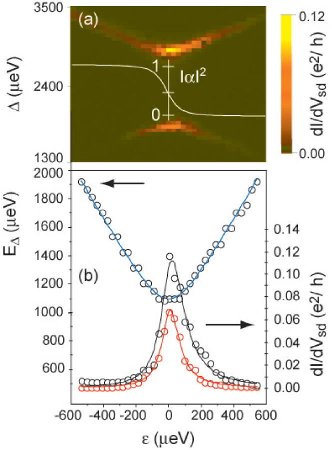
To study the robustness of this approach, we will shortly focus on a region with a larger tunnel coupling, for gate-voltages around mV and mV (this is outside the range shown in Fig. 1(d)). An analysis of the capacitances yields aF, aF, and aF. In the analysis we have used the gate capacitances obtained in Fig. 2, aF, and aF. Figure 3(a) shows the two high-conductance wings plotted versus and . The spacing of the wings, , yields a tunnel coupling of eV and eV, see Fig. 3(b). The maximum differential conductance along the two wings is plotted in Fig. 3(c) and Fig. 3(d). A fit according to Eq. 3-5 yields eV for the top wing and eV for the bottom wing. The probability of finding the electron in the first dot, , is again plotted as an overlay in Fig. 3(a) for an averaged value of eV. For the magnitude of the agreement between the wing spacing and the conductance traces is not quite as good as for the data presented in Fig. 2. However, taking into account the simplicity of the used approach, the results are encouraging. In particular, we emphasize that the wavefunction of the artificial molecule is extended over more than a micron, neglecting the influence of impurities which are likely to be present in the carbon nanotube.
In this article, we have shown that electron delocalization in an artificial molecule can directly be traced by electrical transport measurements. In particular, this technique allows for mapping molecular wave functions of the kind . Our results reflect the close relationship of covalent bonding and efficient electronic exchange, being one of the key challenges to be mastered in molecular electronic devices Reed . For the field of carbon nanotube double quantum dots, the findings represent an additional step towards the controlled engineering of quantum states. Future experiments will have to address the dynamics of the electron spin in carbon nanotube quantum dots, as these may be well-suited building blocks for spin-based quantum computers Burkard .
I acknowledgments
This work was obtained in collaboration with D. Loss and B. Coish. Discussion with them are gratefully acknowledged. We also would like to thank E. Bieri, A. Eichler, J. Furer, V. N. Golovach, L. Grüter, G. Gunnarson and C. Hoffmann for assistance and discussions. We thank the LMN of the Paul-Scherrer Institute for continuous support in Si processing and we further acknowledge financial support from the Swiss NFS, the NCCR on Nanoscale Science and the ‘C. und H. Dreyfus Stipendium’ (MRG).
References
- (1) Present address: Huntsman Advanced Materials, Klybeckstrasse 200, 4057 Basel, Switzerland
- (2) C. Livermore, C.H. Crouch, R.M. Westervelt, K.L. Campman, and A.C. Gossard, Science 274, 1332 (1996).
- (3) R. H. Blick, D. Pfannkuche, R. J. Haug, K. v. Klitzing, and K. Eberl, Phys. Rev. Lett. 80, 4032 (1997).
- (4) L. DiCarlo, H.J. Lynch, A.C. Johnson, L.I. Childress, K. Crockett, C. M. Marcus, M. P. Hanson, and A. C. Gossard, Phys. Rev. Lett. 92, 226801 (2004).
- (5) M. Pioro-Ladriére, R. Abolfath, P. Zawadzki, J. Lapointe, S.A. Studenikin, A.S. Sachrajda, and P. Hawrylak, Phys. Rev. B 72, 125307 (2005).
- (6) A. W. Holleitner, R. H. Blick, A. K. Hüttel, K. Eberl, and J. P. Kotthaus, Science 297, 70 (2002).
- (7) T. Hatano, M. Stopa, and S. Tarucha, Science 309, 268 (2005).
- (8) C. Fasth, A. Fuhrer, M. Björk, and L. Samuelson, Nano Letters 5, 1487 (2005).
- (9) N. Mason, M. J. Biercuk, and C. M. Marcus, Science 303, 655 (2004).
- (10) Sapmaz S, Meyer C, Beliczynski P, Jarillo-Herrero P, and Kouwenhoven LP, Nano Letters 6(7) 1350 (2006).
- (11) M. Gräber, W.A. Coish, C. Hoffmann, M. Weiss, S. Oberholzer, J. Furer, D. Loss, and C. Schönenberger Phys. Rev. B , (2006).
- (12) W. A. Coish and D. Loss cond-mat/0606550
- (13) J. Kong, H. T Soh, A. M. Cassel, C. F. Quate, and H. Dai, Nature 395, 878 (1998).
- (14) at o in a mixture of H2 and CH4 with flow rates of and l/min, respectively.
- (15) W. G. van der Wiel, S. de Francheschi, J. M. Elzermann, T. Fujisawa, S. Tarucha and L. P. Kouwenhoven, Rev. Mod. Phys. 75, (2003).
- (16) R. Ziegler, C. Bruder, and H. Schoeller, Phys. Rev. B 62, 1961 (2000).
- (17) M.A. Reed, C. Zhou, C.J. Muller, T.P. Burgin, and J.M. Tour, Science 278, 252 (1997).
- (18) G. Burkard, D. Loss, and D. P. DiVincenzo, Phys. Rev. B 59, 2070 (1999).