Electronic Interface Reconstruction at Polar-Nonpolar Mott Insulator Heterojunctions
Abstract
We report on a theoretical study of the electronic interface reconstruction (EIR) induced by polarity discontinuity at a heterojunction between a polar and a nonpolar Mott insulators, and of the two-dimensional strongly-correlated electron systems (2DSCESs) which accompany the reconstruction. We derive an expression for the minimum number of polar layers required to drive the EIR, and discuss key parameters of the heterojunction system which control 2DSCES properties. The role of strong correlations in enhancing confinement at the interface is emphasized.
pacs:
72.80.Ga,73.20.-r,71.10.FdI Introduction
Two-dimensional (2D) electron systems have been a fertile source of interesting physics over the past few decades, playing host to the fractional and integer quantum Hall effects and cuprate superconductivity among other phenomena. The most widely studied and most thoroughly understood 2D electron systems are those that occur near semiconductor heterojunctions. In these systems carrier densities and disorder strengths can be adjusted using modulation doping and the electric field effect, and high sample quality can be achieved using lattice matched materials and epitaxial growth techniques. These 2D systems are well described by Fermi liquid theory, at least at magnetic field . Rapid recent progress in the epitaxial growth of complex transition-metal oxidesohtomo2 ; ahn ; keimer ; fitting ; hotta ; ohtomo ; nakagawa ; thiel foreshadows the birth of an entirely new class of 2D electron systems, one in which electronic correlations are strong even at and non-Fermi-liquid behavior is common.
The present authors have recently arguedlee that the modulation doping technique commonly used in semiconductor heterojunction systems can also be applied to complex-oxide heterojunctions to create high-quality two-dimensional strongly-correlated electron systems (2DSCESs) localized near the interface between two different Mott insulators. Our study was based on a generalized Hubbard model which captures some key features of these systems, and on combined insights achieved by applying Hartree-Fock theory (HFT), dynamical mean-field theory (DMFT) and Thomas-Fermi theory (TFT) approaches. This theoretical strategy echoed that adopted by Okamoto and Millisokamoto in addressing the two-dimensional electron systems which can occur near the interface between a Mott insulator and a band insulator. In both cases the properties of the 2D electron systems reflect a delicate balance between space-charge electric fields and strong local correlations.
These 2D systems are clearly unusual in many respects. For instance, their quasiparticles interact with the 3D spin-excitations of the Mott insulator barrier materials. Since researchers now appear to be at the cusp of achieving experimental control over this kind of 2D electron system, it is interesting to explore the possibilities theoretically in an attempt to find useful theoretical frameworks, and hopefully also to partially anticipate some of the new phenomena likely to occur. To mention one example, it has recently been suggested that a spin-liquid insulator could be found in a Mott insulators bilayerrib system with an appropriate doping profile.
The apparent electronic interface reconstruction (EIR) discoveredohtomo ; nakagawa ; thiel at the heterojunction between the band insulators LaAlO3 and SrTiO3 is unique in complex oxide interface studies and does not have an analog in semiconductor heterojunction systems, although there is still some uncertainty about the role of oxygen vacancies in the measured conductivity. For example, it has been proposed pen that the oxygen vacancies are responsible for the insulating behavior observed at the -type interface. The reconstruction is forced by the polarity difference between LaAlO3 and SrTiO3. Polarity discontinuities are normally weaker at semiconductor heterojunctions and, when present, the electric fields to which they give rise are usually screened by relaxation of atoms near the interfacesze . In complex transition metal oxides, however, it was discoveredSawatzky ; nakagawa that the polarity discontinuity field can be screened electronically by transferring electrons between surface and interface layers, changing the valence of transition metal ions in these layers. Electrons dodge the polar catastrophenakagawa without essential atomic assistance. It has been shownthiel that such an interface can be tuned between metallic and insulating states by relatively modest electric fields, suggesting the possibility of novel electronic devices.
In this paper we examine EIR at a heterostructure between model polar and nonpolar Mott insulators. We have in mind for these effects Mott insulators with cubic peroskite structures. Possible materials combinations are discussed in Section VI. The long-ranged Coulombic space-charge fields are treated within the Hartree approximation, and strong on-site Coulomb interactions are treated by solving HFT, DMFT, and TFT equations. We find that a minimum number of polar layers is required to induce an EIR because of strong local correlations, whereas the number of nonpolar layers does not play an essential role in determining the electron distribution. We also find that when a 2D electron system is present near the heterojunction, it is strongly localized because of strong correlations which limit the potential of the electronic system to lower its energy by spreading out in the growth direction. TFT results provide a simple way of understanding the more microscopic DMFT and HFT calculations and are remarkably accurate.
II Single Band Hubbard Model
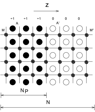
Fig. 1 illustrates the model heterostructure we investigate in this paper. We consider a thin film composed of polar perovskite Mott insulator layers () and nonpolar perovskite Mott insulator layers (), where () is a group III (II) element with a valence of +3 (+2) in the layer. () is a group () element which is a Mott insulator because of strong local repulsion among the d-orbitals. In this study we disregard the interesting complications associated with orbital degeneracy and do not account directly for hybridization between the transition metal and oxygen ions. We therefore use a single band Hubbard model to describe the valence electrons. Long-ranged Coulomb interactions are described realistically by accounting for charges at the oxygen sites and on the , , and , and ions. The resulting model Hamiltonian is:
| (1) |
where labels a metal site and (grouping coplanar oxygen and A cation charges) in the present case. The d-orbital hopping term is expressed in Eq.(1) as a sum over links; most of our calculations have been performed for a model with nearest-neighbor hopping. Second nearest-neighbor hopping has little influence on our main results, but will impact the 2DSCES Fermi surfaces as discussed below. The sizes and alignments of the gaps in the two Mott insulators are fixed by the interaction and site energy parameters: and for the polar layers and and for the nonpolar layers. In an ideal cubic perovskite unit cell with lattice constant , and respectively. The third term in accounts for a net effective charge per atom in the plane; this charge is the sum of the oxygen ion charges and the charge of the ion when in a configuration. In this work we have neglected the uneven distribution of charge within each layer. In this calculation we for the most part assume that is constant, but emphasize that the difference between d-orbital energies on opposite sides of the heterojunction can be an important parameter. As in case of semiconductors, band lineups play a key role in determining heterojunction properties and are likely to be difficult to estimate with sufficient precision. Accurate values will most likely have to be determined experimentally for each heterojunction system considered. The requirement of overall electrical neutrality in the thin film implies that the d orbital occupancy, averaged over the thin film , satisfies .
Throughout this study we use the Hartree approximation for the long-ranged Coulomb interaction and neglect the corresponding exchange term, since our goals in studying this toy model are purely qualitative. The self-consistently determined Hartree mean-field Hamiltonian is
| (2) |
where is the electron density on site , for , and for . In the continuum limit, becomes:
| (3) |
where .
III Hartree-Fock Theory
In HFT the Hubbard term is replaced by its mean-field counterpart: . As pointed out okamoto ; lee previously, there are almost always a number of distinct self-consistent solutions of the HF equations, corresponding to various local-minima and saddle-points of the HF energy functional. Here we present results for solutions with -type antiferromagnetic (AFM) order, or spin order, and ferromagnetic (FM) order. These solutions are representative of ordered states which occur frequently in complex transition metal oxides and are often global minima of the HF energy functional. The philosophy of following this procedure is that HFT can neither reliably judge the competition between different types of order, nor predict whether or not long-range order succumbs to fluctuations. The results nevertheless very often provides a reasonable description of local correlations in the strongly correlated regime.
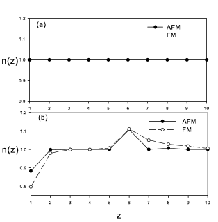
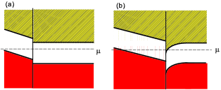
Our HFT results for and are summarized in Fig. 2. For the calculations reported here, the total layer number and typical values were chosen for the interaction parameters. ( and .)okamoto For both AFM and FM states EIR occurs only for the model thin film with the larger value of . This feature is a result of the competition between the polar catastrophenakagawa and strong local correlations. Although the polarity discontinuity at the interface favors a transfer of electrons from the outmost surface to the interface, this charge rearrangement is opposed by the Mott-Hubbard gap. It is instructive to consider space-charge induced band bending diagrams like the cartoon illustration of Fig. 3 which contrasts the and cases. For , the bending of the upper and lower Hubbard bands is not large enough to force the chemical potential at the heterojunction outside the gap region. When more polar layers are grown, eventually crosses the lower Hubbard band of the outermost polar layer and the upper Hubbard band of the nonpolar layer nearest the interface, forcing the occurrence of an EIR. If the top layer of the polar material was a positively charged layer rather than a negatively charged layer, the charge transfer would occur from the lower Hubbard band near the heterojunction to the upper Hubbard band near the surface.
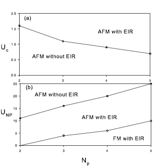
An analogous competition has already been discussed and studied experimentally in LaAlO3/SrTiO3 heterostructures thiel . In that case the energy which competes with the polar catastrophe is the energy difference between the top of oxygen -bands in nonpolar SrTiO3 and the bottom of aluminum bands in LaAlO3, instead of the correlation gap in the example studied here. Since it always costs the gap energy to add more electrons on any layer of the heterostructure, electrons accumulate initially near the interface to gain the most electrostatic energy, eventually spreading out through the heterostructure to minimize kinetic energy cost. Quantum confinement of the 2DSCES associated with EIR is stronger for states with stronger on-site correlations because the kinetic energy is then a smaller component of the overall energy budget. This is the reason that in Fig. 2(b) electrons are more confined to the interface in the AFM state than in the FM state. (The FM state has larger bandwidths and smaller correlation gaps, at least within HFT.) Based on the discussion above, we expect that for fixed and , the minimum number of polar layers required to achieve reconstruction will be smaller when is larger. will also tend to decrease when the Hubbard gap is reduced in either layer; in Fig. 4 we illustrate the dependence on when is fixed. Note that a smaller value of favors ferromagnetic HF states.
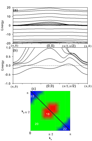
A more microscopic view of EIR is provided in Fig.5 where we illustrate the electronic structure of the AFM solution of the Hartree-Fock equations for a thin film with . The parameters used to construct this illustration are the same as those used for the case in Fig.2(b). The thin film has 20 two-fold spin-degenerate 2D bands because of the reduced translational symmetry of the AFM state, and charge neutrality requires that 10 bands be occupied. In Fig. 5(a) we can identify 10 relatively widely spaced bands which correspond at high energies to the upper Hubbard band and at low energies to the lower Hubbard band in the polar material. The bands are widely spaced because of the average electric field in the polar material; for the same reason these bands are quite highly localized in individual atomic layers. The two groups of more narrowly spaced bands correspond respectively to the upper Hubbard band and the lower Hubbard band of the non-polar material. Because the space-charge electric fields are much either almost fully or at least partially screened out in the non-polar material by charge accumulation at the interface, the bands are closely spaced and the corresponding eigenstates contain more inter-layer characters. When EIR occurs there is a weakly avoided anticrossing between the top-most lower Hubbard band state in the polar material and the upper Hubbard band states of the non-polar material. This anticrossing is apparent in Fig.5(b) which expands the region of the electronic structure close to the Fermi energy. In the ground state the polar lower-Hubbard band state is lower in energy at the Brillouin-zone center but higher in energy toward the Brillouin-zone edges. (For a model with only nearest-neighbor hopping the lower upper band has its maximum and the upper Hubbard band has its minimum along the line from to .)
For the parameters used in this calculation (with second nearest-neighbor hopping ) the EIR leads to two partially occupied 2D bands illustrated in Fig. 5(c), a nearly full lower-Hubbard band very localized on the surface and with two inequivalent hole pockets in the AFM Brillouin zone centered on and and a nearly empty band concentrated on the first non-polar layer with an electron pocket centered on .
IV Thomas-Fermi Theory
Layered oxide materials have a natural Thomas-Fermi approximation in which the total energy is expressed as the sum of the total electrostatic energy and a local-density-approximation for the band and correlation energies. For layered structures the contribution to the energy from each atomic layer is approximated by the energy per layer of an electrically neutral 3D system with the average site occupancy of that layer. Minimizing this energy with a fixed total density constraint leads to the following TF equation:
| (4) |
where for this case is.
| (5) |
and is the overall chemical potential. Following the same approach described in Reflee , we can solve the TF equations for different ordered states using calculated from HF solutions for the three-dimensional Hubbard model. We confirmed that TFT very accurately reproduces the results of HFT for the charge distribution between the layers, as in the case of modulation dopinglee .
One advantage of using this TF equation is that we can derive some key properties analytically. For example, if we assume that the d-orbitals of polar and non-polar sides are both described by one-band Hubbard models and that the charge transfer occurs from a single surface layer to a single interface layer Eq.(4) reduces to
| (6) |
where the Hubbard model chemical potentials are expressed as function of density in units of electrons per atom, is the charge transfer, and the on-site energies which are usually set to zero in Hubbard models, restored on each side of the heterojunction. Since the left hand side is a monotonically decreasing function of and the right hand side is a monotonically increasing function of , this equation has a solution and EIR will occur if
| (7) |
i.e. if the electric potential drop across the polar layer exceeds the spatially indirect gap between the bottom of the upper Hubbard band in the non-polar material and the top of the lower Hubbard band in the polar material. Since the variation of chemical potential with density is strongly reduced outside of the gap in strongly correlated material, it follows that the amount of charge transfered once exceeds the minimum value is given accurately by
| (8) |
As the right hand side of Eq. 8 becomes comparable to 0.5 at larger values of , the fundamental assumption of our simple model (namely that the polar catastrophe is avoided by electronic rather than atomic reconstruction) becomes increasingly suspect. When EIR occurs it is likely to lead to relatively small 2D Fermi surface pockets, as illustrated in Fig. 5.
V Dynamical Mean-Field Theory
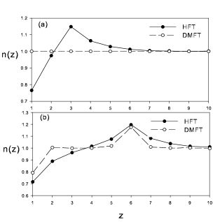
Hartree-Fock theory can describe the physics of strong local correlations only when the correlations are static and lead to FM or AFM ordered states; HF solutions for PM states completely miss local correlation and do not reproduce the Mott-Hubbard gap. DMFT captures correctly the insulating gap created by on-site correlations even for inhomogeneous multilayered systemsokamoto ; lee ; freericks . For this reason DMFT calculations for paramagnetic states (PM) provide important additional insight into EIR in Mott-Hubbard insulator heterojunction systems. For the impurity solver necessary in applications of DMFT, we adopt the simple two-site method proposed by M. Potthoffpotthoff , which has been successfully applied to a variety of different transition metal oxide heterostructuresokamoto ; lee . The results for and are presented in Fig. 6 with and . When a paramagnetic state is described by HFT, charge transfer from the surface to the interface occurs (incorrectly) even for . For , the screening of the surface layer electric field incorrectly begins immediately in the polar material. The DMFT calculations demonstrate that a larger value of is required even if the spin-degree of freedom is not ordered in the Mott insulators. These results confirm that a minimum thickness of polar layers is required for EIR when on-site correlations are strong.
VI Material Considerations
It is not so easy to determine on purely theoretical grounds which material combinations could be used to realize the EIR proposed here. In the family of cubic perovskites, candidate polar materials include LaTiO3 and YTiO3 and possible non-polar materials include SrVO3 include CaVO3. The band offsets of the various possible materials combinations can be estimated from existing electronic structure calculations. LDA calculations based on Wannier functionspavarini indicate that the bands tend to be higher in energy relative to the oxygen levels in LaTiO3 and YTiO3 than in CaVO3 and SrVO3. Assumming that the oxygen levels are closely aligned across the heterostructure, we can expect that LaTiO3 and YTiO3 will have higher orbital energies than CaVO3 and SrVO3. Another interesting observation from the LDA calculations is that energy differences between different orbital associated with distortions of the ideal cubic perovskite structure tend to increase across the series SrVO3-CaVO3-LaTiO3-YTiO3. These additional features related to the orbital degree of freedom may bring in new physics which can not be explored in our single-band thin film model. Moreover, the tendency toward magnetic ordering may also be influenced by the presence or absence of orbital degeneracy, which will in turn be influenced by reduced symmetry near the heterojunction. The same calculations show that CaVO3 and SrVO3 are metallic in the bulk. Lower coordination and electric fields that reduce inter-layer hopping are likely to tip the balance toward the insulating state in thin films and especially near heterojunctions, so these materials are still candidates for realization of the physics studied here.
Although sophisticated first principle calculations can provide some insight and will help with the construction of realistic phenomenological models, the consequences of orbital degeneracy or near-degeneracy for complex oxide heterojunctions may depend on subtle issues of many-particle physics. Another aspect not captured realistically in this qualitative study is the dielectric constant which in general could be a very complicated function of positions throughout the heterostructuressawa . Experimental information when available will likely play an essential role in achieving a full understanding.
One of the most important effect of the band lineups in our model is its influence on where the electrons accumulate when EIR occurs. We have shown that in the case of constant electron accumulation near the heterojunction appears on the first layer. This will change if for the polar materials is low enough so that the sum of and electrostatic potential is minimized at the last layer, instead of the first layer.
VII Summary
In this paper we have studied electronic interface reconstruction (EIR) in polar-nonpolar Mott insulator heterostructure systems. We use a simple one-band Hubbard model supplemented with long-range Coulomb interactions which assumes that the polar catastrophe in layered polar materials is avoided by electronic rather than lattice reconstruction. We find that EIR occurs only if a thin film contains a minimum number of polar layers ; when model paramaters representative of perovskite oxides are chosen . In this paper, the electronic structure of polar-non-polar Mott insulator heterojunctions was investigated using Hartree-Fock theory (HFT), Thomas-Fermi theory (TFT), and dynamical mean-field-theory (DMFT). Using TFT we are able to derive an analytical expression for the dependence of EIR on model parameters, which may be useful in selecting suitable materials. For polar and non-polar Hubbard interaction parameters ( and respectively) a stronger Coulomb interaction parameter will reduce , while for and fixed, larger will increase . Strong on-site correlations enhance quantum confinement of the interface states which accompany EIR, resulting in 2D systems that are nearly completely confined to an atomic plane. When the Mott insulator barrier materials have antiferromagnetic order, Hartree-Fock calculations demonstrate the emergence to 2D electron systems with Fermi surface areas and characters that depend sensitively on the details of the model. The quasiparticles of this system will differ from ordinary 2D electron systems because they will interact strongly with the 3D spin excitations of the antiferromagnetic Mott insulators. The unusual properties suggest the likelihood of interesting non-Fermi liquid states in some regions of the model’s parameter space.
We have also discussed some possible material combinations which might lead to the EIR we envision and the key role of the alignment of d-orbital energies across the heterojunction. Some realistic features of perovskites, for example, orbital degeneracy and lattice distortions, are not captured by the simplified model used in this work. We note that the exchange term from the long-ranged Coulomb interaction, which we have neglected in this study, should enhance the correlation gap. As a result, the charge distribution may be somewhat different if this term is also treated self-consistently. These features of realistic systems are likely to play an important role in practice, especially so when the charge transfer from the surface to the interface region is large enough to sensibly alter the chemical bonding as discussed previously for the Mott-Insulator/Band-Insulator heterojunction casehamann .
In our view, it will likely never be practical to attempt a complete and accurate description of complex oxide interfaces of any type from first principles. Insights from ab inito theory, simplified tight-binding models, and most critically from experiment are all likely to play a role in achieving robust, predictive, phenomenological models of these systems. This work is intented as a step toward establish the correct form of useful phenomenologies.
This work was supported by the National Science Foundation under grant DMR-0606489 and by the Welch Foundation. The authors acknowledge helpful interactions with Harold Hwang, George Sawatzky, and Charles Ahn.
References
- (1) A. Ohtomo, D.A. Muller, J.L. Grazul, and H.Y. Hwang, Nature 419, 378 (2002).
- (2) C. H. Ahn, J.-M. Triscone, and J. Mannhart, Nature 424, 1015 (2003).
- (3) J. Chakhalian, J.W. Freeland, G. Srajer, J. Strempfer, G. Khaliullin, J.C. Cezar, T. Charlton, R. Dalgliesh, C. Bernhard, G. Cristiani, H-U. Habermeier and B. Keimer, Nature Physics 2, 244 (2006).
- (4) L. Fitting, Y. Hotta, T. Susaki, H. Y. Hwang, and D. A. Muller, Phys. Rev. Lett. 97, 256803 (2006).
- (5) Y. Hotta, Y. Mukunoki, T. Susaki, H. Y. Hwang, L. Fitting, and D. A. Muller, Appl. Phys. Lett. 89, 031918 (2006).
- (6) A. Ohtomo and H.Y. Hwang, Nature (London) 427, 423 (2004).
- (7) N. Nakagawa, H. Y. Hwang, and D. A. Muller Nature Materials 5, 204 (2006).
- (8) S. Thiel, G. Hammerl, A. Schmehl, C.W. Schneider, and J. Mannhart, Science 313, 1942 (2006).
- (9) W.-C. Lee and A.H. MacDonald, Phys. Rev. B 74, 075106 (2006).
- (10) S. Okamoto and A.J. Millis, Nature (London) 428, 630 (2004); S. Okamoto and A.J. Millis, Phys. Rev. B 70, 241104 (R) (2004); S. Okamoto and A.J. Millis, ibid. 70, 075101 (2004).
- (11) T. C. Ribeiro, A. Seidel, J. H. Han and D.-H. Lee, Europhys. Lett. 76, 891 (2006).
- (12) R. Pentcheva and W.E. Pickett, Phys. Rev. B 74, 035112 (2006); Min Sik Park, S.H. Rhim, and Arthur J. Freeman, Phys. Rev. B 74 205416 (2006).
- (13) S. M. Sze, High Speed Semiconductor Devices Wiley, New York, (1990).
- (14) R. Hesper, L. H. Tjeng, A. Heeres, and G. A. Sawatzky, Phys. Rev. B 62, 16046 (2000).
- (15) J.K. Freericks, Phys. Rev. B.70, 195342 (2004); J.K. Freericks, V. Zlatic, and A.M. Shvaika, ibid 75, 035133 (2007).
- (16) M. Potthoff, Phys. Rev. B 64, 165114 (2001).
- (17) E. Pavarini, A. Yamasaki, J. Nuss, and O.K. Andersen, New J. of Phys. 7, 188 (2005).
- (18) S. Altieri, L.H. Tjeng, F.C. Voogt, T. Hibma and G.A. Sawatzky, Phys. Rev. B 59 R2517 (1999).; J. van den Brink and G.A. Sawatzky, Europhys. Lett. 50 447 (2000).
- (19) D. R. Hamann, D. A. Muller, and H. Y. Hwang Phys. Rev. B 73, 195403 (2006); S. Okamoto, A. J. Millis, and N. A. Spaldin Phys. Rev. Lett. 97, 056802 (2006)