Nonequilibrium Noise in Low-doped Manganite Single Crystals
Abstract
noise in current biased La0.82Ca0.18MnO3 crystals has been investigated. The temperature dependence of the noise follows the resistivity changes with temperature suggesting that resistivity fluctuations constitute a fixed fraction of the total resistivity, independently of the dissipation mechanism and magnetic state of the system. The noise scales as a square of the current as expected for equilibrium resistivity fluctuations. However, at 77 K at bias exceeding some threshold, the noise intensity starts to decrease with increasing bias. The appearance of nonequilibrium noise is interpreted in terms of bias dependent multi-step indirect tunneling.
pacs:
72.70.+m Noise processes and phenomena, 72.15.-v Electronic conduction in metals and alloys, 73.43.Jn Tunneling, 75.47.Gk Colossal magnetoresistanceA fundamental interest in mixed-valence manganese perovskites arises from their strongly spin-dependent conductivity and pronounced manifestations of phase separation (PS). In a complex and rich phase diagram of La1-xCaxMnO3 (LCMO) manganites the critical doping level separates ferromagnetic (FM) insulating ground state at from FM metallic ground state above . In the doping range x a mixed FM state composed of insulating and metallic FM phases with different levels of orbital ordering appears below Curie temperature .papa Therefore, physical mechanisms dominating transport properties of low-doped LCMO, , became remarkably different when the temperature is changing. Hopping conductivity controls transport in the paramagnetic (PM) insulating regime at . Intrinsic PS associated with metal-insulator (M-I) transition at leads to percolation conductivity in the FM state at . Low temperature resistivity is likely dominated by tunneling across intrinsic barriers associated with extended structural defects, such as twins and grain boundaries, and/or with inclusions of insulating FM phase interrupting metallic percolating paths.prb018
Noise measurements are known to provide a unique insight into dynamics of solid state systems. A peak of the noise resulting from the percolating transition around was found in various manganite thin films.podzorov ; reutler ; ziese Grain boundary junctions were identified as sources of noise in manganite thin films.gross Non-gaussian random telegraph fluctuations were ascribed to PS at low temperatures.raquet ; merithew
In such complex system as low-doped LCMO one expects that noise data will allow to get a deeper insight into the dynamics of dissipation processes associated with different transport mechanisms. In this paper we report on electric noise properties in dc current biased low-doped LCMO single crystals which include the appearance of nonequilibrium noise at low temperatures.
The experiments were performed with La0.82Ca0.18MnO3 single crystals grown by a floating zone method, as described elsewhere.prb018 As grown crystals were cut into individual samples in the form of thin bars with the longest dimension along the crystalline direction. Current and voltage leads were attached to pre-evaporated gold contacts by a conducting silver epoxy bound. Current-voltage characteristics , differential resistance , and noise spectra were measured at various temperatures using a standard four-point contact arrangement. The measurements reported here were all performed at zero applied magnetic field.
For noise measurements the voltage drop across dc current biased sample was amplified by a home made very low noise preamplifier placed directly on the cryostat top, and processed by a dynamic signal analyzer. Instrumental noise originating from the measuring chain was eliminated by subtracting the reference spectrum, recorded at zero current flow in the LCMO sample, from the spectrum acquired with bias current. Possible contact contributions to the noise were excluded by using a high impedance ballast resistors in series with dc current source.
The temperature dependence of the resistivity measured under low dc current bias of 10 A is shown in Fig. 1. At the sample is in PM insulating state. At the temperature of metal-to-isolator transition at K, coinciding with PM to FM transition, the reaches a local maximum.prb018 Below the ferromagnetic metallic state forms percolating conducting paths in the insulating matrix and the resistance decreases with decreasing temperature. The low temperature upturn at temperatures below K can be ascribed to the increasing influence of intrinsic tunneling.
The noise spectra were recorded at different bias currents at temperatures of 77 K, 126 K, 150 K (close to ), 175 K, 185 K, 225 K (in the vicinity of expected Jahn-Teller structural transition) and 290 K. 126 K, 175 K, and 185 K are the temperatures at which the sample has the same resistance under much different dissipation mechanisms. A typical experimental voltage noise power spectral density (PSD) is shown in the inset to Fig. 1. In the entire experimental range of temperatures and currents we have observed with and only at highest currents exceeding 5 mA, as high as 1.5 was recorded at K.
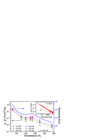
Temperature dependence of the noise shown in Fig. 1 seems to follow temperature changes of the resistance, independently of in the dominating conduction mechanism and magnetic state of the system. If the observed noise is due to current independent resistivity fluctuations which are only probed by the current flow (equilibrium noise) then the PSD should scale as , where is a temperature dependent constant. Data in Fig. 2 obey the above relation at all temperatures with the exception of the 77 K. Noise intensity at 77 K initially increases as but around 1 mA starts to decrease. The decreasing character is temporarily suspended by a local noise increase around 2.75 mA and, eventually, at high currents above 4 mA the noise intensity starts to increase again. The increase at high currents however, is accompanied by significantly higher PSD exponent . Joule heating by the current flow has been excluded as a possible origin of the noise behavior at low temperatures by independent measurements of the resistance and magnetic susceptibility at 77 K as a function of bias current. Noticeable heating effects appeared only at bias currents exceeding 10 mA.
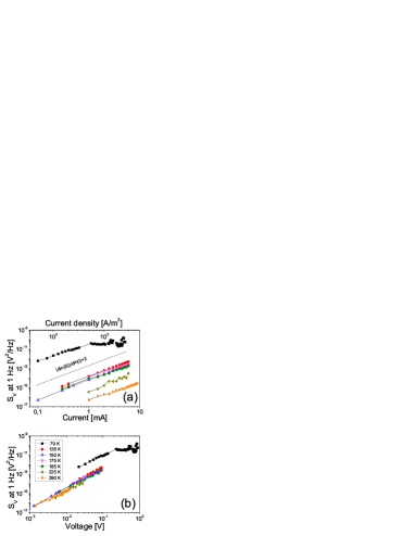
One can collapse the data from Fig. 2a, again with the exception of 77 K points, to a single line by plotting as a function of bias voltage, see Fig. 2b. The collapsed data fit the power law with Hz-1. This fact sheds some light on the fluctuation mechanism. means that the normalized , where PSD of resistance fluctuations, , is current and temperature independent. Since varies strongly with temperature, by more than two orders of magnitude, means that at all temperatures the resistivity fluctuation equals to a fixed fraction of the resistance, . This is quite a surprising result considering remarkable changes occurring in the magnetic state and dissipation mechanism of the sample with changing temperature. Nevertheless, the fact that current flow can actually depress the noise at low temperatures is even more astonishing.
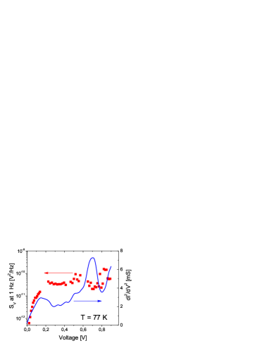
Adopting a point of view that low temperature transport in La0.82Ca0.18MnO3 crystals is dominated by intrinsic tunneling we plot the intensity of the noise at 77 K together with the derivative of the conductance as a function of bias voltage in Fig. 3. We find correlations between behavior of the noise and , which is known to be related to the density of states involved in the tunneling process. At low bias the noise increases, as the square of the voltage, until the first peak of at V. Above 0.17 V the noise does not increase with bias and even decreases in a certain bias range. The noise behavior can be related to underlining fine structure in . However, above the pronounced peak at V the noise starts to increase again.
In general, a peak in is a signature of a step-like conductivity increase. One can therefore attribute peaks to openings of additional tunneling channels with higher conductivity, as predicted by theoretical models of indirect nonelastic tunneling through a chain of localized states.GM ; beasley At low bias voltages the direct and resonant tunneling mechanism dominate. At higher voltages the probability of indirect inelastic tunneling is much higher than that of direct tunneling. The number of involved localized states increases with increasing bias or with increasing barrier width.GM ; beasley The conductivity of an inelastic channel increases with increasing and is exponentially higher than the conductivity of a direct tunneling channel. Eventually, at very high bias levels, or in very wide barriers, the variable range hopping (VRH) becomes more favorable than inelastic tunneling processes.beasley Let us underline that in the investigated system the force exercised by electric field of the bias can directly influence the topology of PS by stretching insulating FM phase and thus increasing the effective width of intrinsic tunnel barriers.viret
Within this scenario the physical mechanism responsible for decrease of the noise with increasing current can be the following: In solid state systems, and in particular in metals and tunnel junctions, noise is known to result from incoherent superposition of many elementary two-level fluctuators (TLF) associated with defects and charge traps. Each TLF generates an elementary random telegraph signal (RTS) with Lorentzian spectrum. The resulting noise will have spectrum in the frequency range in which the distribution of cut-off frequencies within an ensemble is . For thermally activated TLF the latter condition is equivalent to a requirement of a flat distribution of activation energies. The maximum power is dissipated by a symmetric TLF, i.e., by a fluctuator for which the average lifetimes in both RTS levels are equal. Whenever a TLF becomes asymmetric, the intensity of its Lorentzian spectrum is depressed. As a result, noise decreases with increasing asymmetry of elementary fluctuators.
For elementary fluctuators associated with charge traps within a tunnel barrier, the RTS levels can be identified with empty and loaded states of the trap. Electrostatic field of the charge trap modulates the height of the tunnel energy barrier, and consequently the resistivity of the junction, according to the trap occupancy state.
Let us assume that all involved traps are symmetric in their pristine state. It is easy to imagine that electric field of the applied bias stresses and tilts energy structures of trap-based TLFs and renders them asymmetric. noise will decrease with increasing TLF asymmetry due to increasing bias when tunneling current flows across a channel containing stressed traps.
We tentatively interpret the first peak with a transition from a direct to indirect tunneling. Observe that in the elastic tunneling process charge carriers loading the TLF traps are separated from those constituting the tunneling current. This is not necessarily the case in inelastic tunneling.
Opening of an inelastic tunneling channel with higher is marked by a peak in . Local noise maxima at the same bias may be attributed to partition-like noise associated with additional degree of freedom: a possibility of conducting current through competing alternative channels. When the voltage becomes sufficiently high to activate the VRH the noise again increases with bias. Indeed, is predicted by the model of noise in VRH regime.shklovski
Obviously, in a difference to a discrete fabricated tunnel junction, or to a single grain boundary junction, gross one cannot provide an absolute direct proof of the tunnel character of the bulk conductivity dominated by distributed intrinsic junctions. Only an indirect evidence can be brought from observations of nonlinear voltage-current characteristics and their temperature evolution, provided both can be well fitted to a tunneling model. In our previous paper on metastable nonlinear resistivity in LCMO crystals we have well fitted the experimentally observed characteristics to the indirect tunneling model.prb018
In conclusion, we have observed equilibrium voltage noise in a wide range of currents and temperatures corresponding to markedly different magnetic and transport properties of the system. At low temperatures where transport is dominated by tunneling mechanism the nonequilibrium noise appears and decreases with increasing bias due to bias imposed stress of elementary TLFs participating in inelastic tunneling.
This work was supported by Israel-Korea bilateral program. X.D.W. acknowledges support of Monash University ”Taft Fellowship” and M.B. of the Russian-Ukrainian research program ”Nanophysics and Nanoelectronics”.
References
- (1) G. Papavassiliou, et al. Phys. Rev. Lett. 91, 147205 (2003).
- (2) Y. Yuzhelevski, et al. Phys. Rev. B 64, 224428 (2001).
- (3) V. Podzorov, et al. Phys. Rev. B 64, 115113 (2001).
- (4) P. Reutler, et al. Phys. Rev. B 62, 11619 (2000).
- (5) D. S. Rana, et al. Phys. Rev. B 74, 094406 (2006).
- (6) J. B. Philipp, et al. Phys. Rev. B 66, 224417 (2002).
- (7) B. Raquet, et al. Phys. Rev. Lett. 84, 4485 (2000).
- (8) R. D. Merithew, et al. Phys. Rev. Lett. 84, 3442 (2000).
- (9) L. I. Glazman and K. A. Matveev, Sov. Phys. JETP 67, 1276 (1988).
- (10) Yizi Xu, et al. Phys. Rev. B 52, 2843 (1995).
- (11) M. Viret, et al. Phys. Rev. B 72, 140403 (2005).
- (12) B. I. Shklovskii, Phys. Rev. B 67, 045201 (2003).