Mesoporous matrices for quantum computation with improved response through redundance
Abstract
We present a solid state implementation of quantum computation, which improves previously proposed optically driven schemes. Our proposal is based on vertical arrays of quantum dots embedded in a mesoporous material which can be fabricated with present technology. The redundant encoding typical of the chosen hardware protects the computation against gate errors and the effects of measurement induced noise. The system parameters required for quantum computation applications are calculated for II-VI and III-V materials and found to be within the experimental range. The proposed hardware may help minimize errors due to polydispersity of dot sizes, which is at present one of the main problems in relation to quantum dot-based quantum computation.
I Introduction
The current high level of progress in the design and manufacture of low dimensional structures, has led to an increasing interest in the development of solid state based quantum computingneilsenchang schemes/hardware. Among the various proposals are schemes which rely on spin and exciton qubits confined in semiconductor quantum dots (QD)PhysToday , which can be manipulated using ultra fast laser pulseschapter . Several of these optical quantum computation schemes rely on exciton-exciton direct Coulomb interaction, which provides the necessary coupling to perform two qubit gatesirene ; gan . The presence of an exciton in a QD produces a biexcitonic shift in the ground state excitonic energy of a nearby QD. By driving a qubit at this shifted frequency conditional operations can be performedirene ; gan .
In order to carry out practical quantum computation it is necessary to be able to address individual qubits. This poses a problem for driving optically the response of self assembled quantum dot ensembles (such as the ones grown by Stranski-Krastanow techniques): in these ensembles the size of each dot is one order of magnitude smaller than the laser spot addressing it. To this end it has been proposed to use energy selective methods on isolated stacks of quantum dots (quantum registers)irene ; gan . However, it is still experimentally difficult to control QD size and position in a satisfactory way, and QD vertical stacks tend to form in the plane at random positions. Additionally the size of the QDs within the stacks is hardly controllable, resulting in the practical difficulty of creating the desired sequences of energy selectable excitonic transitions.
In the past years, techniques and materials have been developed that may allow to solve most of the fabrication issues associated with stacked quantum dot arrays. For example, materials like MCM-41 and SBA-15 consist of regular arrays of pores forming a hexagonal lattice889 ; 696 ; 8989 . By simple variations of the synthetic conditions, the pore diameter can be varied from a few nm to tens of nm. The thickness of the oxide walls separating the pores can also be varied, from about 1 nm to ca. 6 nm 10001 . While the first materials of this kind were based on silicates, more recently matrices with a well-defined pore size and pore arrangement have been reported also for high dielectric constant materials such as ZrO2 10002 ; 10006 , and mixed Si-Ti oxides 10003 ; 10004 ; 10005 ; nonhydro . Metal and semiconductor nanoparticles can be grown within the pores of these materials with techniques as varied as calcination 676 , photolithography bertino ; Gadipalli ; Gadipalli2 , and electrochemistry1276 ; final . With these techniques, superlattices of quantum dots have been produced 673 . The electrochemical route is probably the most interesting for the scheme that we propose. The group of M. Natan has demonstrated that stacked arrays of metals can be fabricated inside porous materials. Columns with a height of up to 15 m made up by up to 8 stacked layers have been obtained 1276 . In the future, it may be possible to fabricate composite materials made up of several layers of semiconductors disposed on a hexagonal lattice. The height of the dots within each layer will be controlled by the processing conditions (e.g., electrodeposition time) while the lateral size of the dots will be determined by the matrix pore size. The coupling between dots in different pores will be tuned by varying the wall thickness and/or by varying the dielectric constant of the oxide making up the walls.
II System and Redundant Encoding
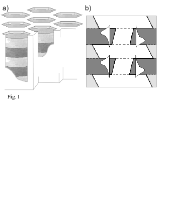
We consider a system consisting of a TiO2 matrix in which alternating layers of two semiconductors with widely different band gaps are deposited. This provides a stack of QDs (qubits), sandwiched between the larger band gap material (barriers). The resulting system is depicted in Fig. 1(a) and consists of an array of identical, hexagonally packed stacks of quantum dots (columns). The band structure within each column is sketched in Fig. 1(b). As shown in sec. III the distance between nearby columns, and the high dielectric constant ()TiO2 of the matrix is sufficient to consider each stack as isolated from its neighbors.
We propose to use semiconductors which can assume wurtzite crystal structure. This leads to a strong intrinsic electric fieldpiezo , which enhances coupling between excitons in neighboring quantum dots within a stackgan . We calculate the built-in electric fields inside the quantum dots by considering an alternating sequence of quantum wells and barriers: results are in good agreement with experimental findingsgan , showing that the lateral shape of the dot is mainly responsible for the strong in-plane carrier confinement. Quantum computation can then be carried out by using sequences of laser pulses, as described in Ref. chapter, . Under the influence of the same laser pulse, each column will act as an independent replica of the same computational array. The advantage of the hardware we propose is this intrinsic redundance.
A practical quantum computing scheme must include some error-correction strategy for errors due to computation or hardware faults. A possibility is to average over many individual occurrences of the same quantum algorithm, so that fluctuations around the expected result are protected against. An example of this is seen in nuclear magnetic resonance (NMR) schemesNMR , where large ensemble of qubit arrays are naturally available. In the current work we propose a somewhat analogous, but solid state based, ensemble. The ensemble is constituted by the quantum dot columns uniformly distributed within the matrix. The advantage of our solid state ensemble over NMR ones is twofold, namely the ability to initialize all arrays in the ensemble to a known well defined state – the ’no-exciton’ ground state – and the intrinsic order of our ensemble, which e.g. allows for a certain degree of spatial addressability. In this respect we mention that on the micrometer scale, different semiconductors can be deposited with photolithographic techniques on areas of the matrix, to create regular supra-arrays of selected geometries, e.g. hexagons or stripesbertino ; Gadipalli ; Gadipalli2 . We foresee that this property might be used to perform different calculations on different areas of the matrix. The envisaged possibility of growing relatively long arrays, i.e. quantum registers of the order of some tens of qubits (QDs), is another advantage over NMR based systems.
III Theoretical Model and Calculated Parameter Range
To check the feasibility of the proposed scheme, we model each individual stack as a column of cylindrical quantum dots with the same radius. To calculate the biexcitonic shifts, the confining potentials are modeled as parabolic potentials with the same characteristic widths as the expectation values and of the cylindrical dots in the stack. Nearby quantum dots are coupled by the biexcitonic shift between ground state excitons. In order to calculate the correct parameter space, we approximate the biexcitonic shift as
| (1) |
where is the wavefunction of the exciton in QDi in the single particle approximation, and is the Coulomb interaction between the two excitons.
In the proposed hardware, the stacks are separated by the matrix walls, which can currently be made up to nm thick whilst maintaining the order of the structure. To be negligible, the inter-stack interaction must be much smaller than the interaction between excitons within a column, i.e. . As we will show below, both II-VI and III-V based systems can be designed so that there is more than an order of magnitude difference between the two energy scales, whilst mantaining the matrix walls within the experimental range.
If all the stacks in the ensemble were to compute correctly – i.e. no computational errors – inter-stack interactions would only renormalize the excitonic energies by the same amount for each stack, which could be easily accounted for in the computational scheme. However the event of computational failure in a certain stack will induce a local, unwanted, shift of the exciton energies in neighbouring stacks. Each individual stack will interact with a certain number of such ’faulty computing’ stacks. Therefore the magnitude of this unwanted shift is the sum of the interaction energies of a resident exciton with an exciton in each ’faulty computing’ stack. The stacks are arranged in a hexagonal structure, which can be represented as a series of concentric hexagonal shells surrounding each stack. The th shell consists of stacks. The number of expected computational failures in the th shell will therefore be , where is the probability of a successful computation for any individual stack. We estimate the total energy shift due to interactions with all the ’faulty computing’ stacks in the ensemble as:
| (2) |
where is radius of the th hexagonal shell, and being the maximum and minimum distance of the shell from the central stack. is calculated according to Eq. (1).

In Fig. 2 we show the results for system parameters appropriate for implementing computational schemes. As a typical GaN/AlN system, we consider nm porous radius with QD height nm and barrier width nm; As a typical CdSe/CdS system we consider nm porous radius with QD height nm and barrier width nm. It will be shown later in this section that these parameters are indeed appropiates to our scopes. Fig. 2(a) and Fig. 2(b) correspond to the GaN/AlN and CdSe/CdS systems respectively with matrix wall thickness of nm. It can be seen that for GaN QDs (panel a), each stack in the ensemble can be considered isolated for and indeed for whichever value (not shown). corresponds to an average of two failures among the nearest neighbors. For CdSe QDs (panel b) the ensemble can be considered isolated for . Fig. 2(c) and Fig. 2(d) show the same calculation but for different wall thicknesses. In the GaN/AlN system even for matrix walls as thin as nm and , stacks can be still considered isolated (panel c); for the CdSe/CdS system with matrix walls of nm (panel d), the individual stacks can be considered isolated for only. Our results show that that each system can be designed so that individual stacks can be considered isolated for realistic wall thicknesses and a probability of success for a single stack which is reasonably low in CdSe/CdS and can be arbitrarily low in GaN/AlN.
The biexcitonic shift between neighbouring qubits within a stack can be exploited to perform two-qubit gates using multicolor train of laser pulsesirene ; gan ; paulibl . For performing operations on picosecond time scales – which is essential due to the relatively short excitonic decoherence times – must be of the order of a few meV. When choosing the correct parameter range however, additional factors must be taken into considerationirene . Larger can be induced by increasing the height of the quantum dots. This increases the excitonic dipole moments under the influence of the intrinsic electric field. Care must be taken however in allowing at the same time for a satisfactory oscillator strength. Finally the barrier width must be large enough to ensure that single particle tunneling between stacked quantum dots is negligible on the relevant time scales. The tunnelling time is calculated by taking the inverse of the tunneling rate in Ref. storage, .
Fig. 3 shows the range of barrier widths and QD (qubit) heights which satisfy all of the above conditions. The constraints on the system paramaters are , oscillator strength , tunneling time and , where the latter is the ratio between the inter-column to the intra-column exciton-exciton interaction energy.

We have considered both II-VI and III-V heterostructures, specifically CdSe QD and CdS barrier (panels a and b), and GaN QD and AlN barrier (panel c). Panel a) shows the parameter space for a CdSe/CdS system with nm matrix walls, and . Panel b) corresponds to the same system but for . It can be seen that the parameter space is reduced by the requirement of negligible interaction among different QD stacks. Decreasing and/or the wall thickness increases the inter-column interaction, so that the region in parameter space corresponding to low values of is ’cut off’. For large and/or wall thickness the shape of the CdSe/CdS space would be similar to the GaN/AlN case (panel c). For a wall thickness of nm this occurrs at . For reasonable values of and wall thickness, due to the low interstack coupling in the III-V system, the request that different stacks do not interact does not affect the parameter space. Our results show that for both systems there is a wide range of dot sizes, which produce a suitably large biexcitonic shift in the absorption spectrum of the quantum dot. The compatible parameter space in the II-VI system corresponds to taller QDs than the III-V case. This is due to the intrinsic electric field being smaller in the CdSe/CdS system than in GaN/AlN. Therefore larger dot heights and barrier widths are needed to displace the electron and hole wavepackets to provide sufficient coupling between excitons.
Synthesis of II-VI QDs is generally speaking easier than synthesis of of their III-V counterparts. However it has been shownefros that due to the electron-hole exchange interaction the ground excitonic state of materials with wurtzite structure is optically passive, the separation between bright and dark exciton being too large in II-VI systems to be negligible in respect to the energy scales we consider. To overcome this problem, we suggest to consider an n-doped structure such that each quantum dot traps a single electron. As demonstrated experimentally for III-V materialsexperimentalndoped , the exchange splitting can in this way be switched off. This would allow for implementation of schemes such as the one described in Ref. paulibl, , where the spin of the excess electron is the qubit and excitons are used for two qubit gating. It has been shown that for dots in the strong coupling regime, the wave function of the ground state exciton is not significantly affected by the presence of an extra electronpaulibl . Its effect on the biexcitonic shift, which depends on the shape of the excitonic wave functions, can then be safely neglected. Experimentally a possible way of doping each dot with exactly a single electron has been found by doping a QD ensamble with an electron density which matches the dot density. Due to the strong Coulomb repulsion, double occupancy of the dot is avoided. A similar solution could be used to dope the dots in our structure. We envisage an alternative method, which could improve also detrimental stochastical effects. We suggest to apply a bias between the top and the bottom of the structure. In this way each dot would be occupied by exactly one dot starting from the bottom and upwards. For not too strong biases Coulomb blockade would in fact prevent more than one electron occupaying each dot. Once the process has been completed, the bias would be removed and the computational process could begin. As a possible alternative to doping, we can consider CdSe QDs with radii greater than 5nm, for which the exchange splitting becomes very smallefros . These QDs fit well into the parameter space described in Fig. 3.
IV Protection against errors and noise through redundant encoding
As shown above, each individual stack in the structure we propose will behave as an isolated computational register in which quantum operations such as entanglement can be carried out using an appropriate sequence of (sub)picosecond laser pulsesirene ; gan ; paulibl . An appropriate modulation of the QD heights (done as the stack is grown) will result in a different ground state exciton energy (or sequence of energiesLovett ) for each QD in a stack. This allows each qubit in a stack to be selectively addressed and arbitrarily rotated around the Bloch sphere by laser pulses of the appropriate frequency, duration and phase. Similarly conditional two-qubit operations (e.g. entanglement) can be performedirene ; gan ; paulibl .
Our hardware could be used to implement quantum algorithms. The final phase of the algorithm would be to make a measurement on the qubits, generally in the computational basis, to obtain the ’answer’. The measurement of an qubit output, consists of individual measurements, each of which will be found in either the or state. For each individual qubit, being part of an ensemble provides protection against computational errors and measurement noise. In the following discussion we will focus for simplicity, on a single qubit output and assume that before measurement, the qubit is stored in a particular QD which we will refer to as a ’storage’ qubitstorage . For simplicity we will think of it as the upper QD in the stack, though this is not a necessary condition.
After initial preparation (all qubits are initialized in the state, i.e. no excitons present), the driving laser beam will illuminate a circular section of hexagonally packed stacks: this ensemble of stacks represents our redundantly encoded ensemble, since the train of laser pulses will simultaneously drive the same operations on all the stacks of the ensemble. Finally the result from the ensemble is stored in the upper (storage) qubits and may be read off.
In the event of a perfectly successful algorithm with no errors, the entire ensemble of storage qubits would all be in the correct state, which we will assume without loss of generality, to be the state. In reality however, there is a possibility that the quantum algorithm will fail on any one stack. This leads to storage qubits being in the correct state after the computation. Let us assume that in measuring the storage qubit ensemble, the output signal (e.g. photons from excitonic recombination, variation of current through a narrow contact…) is proportional to and in particular a signal will be measured within the range (corresponding to all storage bits being in the ’wrong’ state, e.g. the state) to (corresponding to the whole ensemble in the state). In the hypothesis that the quantum registers (columns) are uncorrelated, the actual signal would be then where we have set the zero signal at . There will also be fluctuations about this value due to noise induced during measurement. In the following we derive a simple relationship to estimate the required ensemble size to correct for given error probabilities. In particular we want to demonstrate that with a modest ensemble of (corresponding to the area illuminated by a laser at optical frequencies, with a spot of diameter Å), it is possible to correct for sizable errors both in the computation and due to measurement noise.
Let us assume that the probability of a successful computation in an individual stack of qubits is constant across the entire ensemble. For an ensemble of stacks of qubits, the probability distribution of obtaining correct answers is binomial
| (3) |
If we assume that in the event of a failure the state of the qubit is found to be in the state with probability , the probability distribution becomes
| (9) | |||||
where denotes how many failed computations have been randomly assigned the correct output. This can be shown to be equal to
| (10) |
which is of the same form of Eq. (3). The shift of the mean value and standard deviation, from those of the probability distribution (3) is due to the fact that for a binomial distribution, even in in the event of a failure there is a finite probability of obtaining the correct result. For a large ensemble of dot stacks, the binomial distribution can be approximated by a Gaussian distribution. The probability distribution (10) under the Gaussian approximation yields a mean value of and a standard deviation of . If the size of the ensemble satisfies
| (11) |
then the result (i.e. ) from a single measure of the ensemble will indicate that the answer from the computation is ( otherwise) with probability % for .

In Fig. 4 we plot the minimum value of N which satisfies Eq. (11) for in respect to the probability of individual success . Here we assume no systematic bias, so we set . The figure shows that, due to the redundant encoding, even when each individual stack computes correctly with a probability as low as , an ensemble of stacks is sufficient for measuring the correct answer with such a high confidence. As discussed in section III, the values of for which our computational scheme applies depend on the thickness of the matrix walls and system materials. For a CdSe/CdS system with nm matrix walls the computational scheme only works for , however for a GaN/AlN system with nm walls the scheme is valid for all .
Let us now consider that experimentally there will always be a certain amount of noise associated to the measurement, and discuss how the redundant encoding can help in tolerating this source of error. We can describe this noise by modifying Eq. 11 as
| (12) |
where and . Again, if N satisfies Eq. (12) with , then a measured signal ensures that the result of the algorithm is with a probability of %. By rearranging Eq. (12) we obtain the condition
| (13) | |||
| (14) |
Setting in Eqs. (13) and (14), gives a lower bound on the ensemble size for the case of a noiseless measurement. For the size of the ensemble needed to correct for this noise tends to infinity. The inset of figure 4 shows that for an ensemble of N=100 stacks, for and , the system is robust even for a measurement noise as high as .
We underline that, using the proposed fabrication method, corresponds to the smallest laser beam spot, solving the problem of spatial addressability in QD-based quantum computing schemes.
V Conclusions
A scheme for implementing quantum algorithms with improved response through redundancy has been presented. Our proposal is based on a mesoporous matrix which provides an uncorrelated ensemble of computational arrays. Our method protects against both computational errors and measurement induced noise, and, using relatively small ensemble sizes, correct answers are found with probability greater than 0.997. Our hardware and computational scheme alleviate many issues of quantum computing schemes based on semiconductor QDs. In these schemes, a major error source is the uncontrolled polydispersity of dot sizes due to the experimental growing techniques. This directly affects the quantized energy levels, detuning them from the ideal ones. We foresee that our scheme can provide a feasible way for containing this source of error.
References
- (1) For a general review on quantum computation, see e.g M. A. Nielsen and I. L. Chuang ”Quantum Computation and Quantum Information” (Cambridge University Press 2000)
- (2) P. M. Petroff, A. Lorke, and A. Imamoglu, Physics Today 54, issue 5, 46 (2001).
- (3) see e.g. ”All-Optical Schemes for Quantum Information Processing with Semiconductor Macroatoms” I. D’Amico, E. Pazy, P. Zanardi, E. Biolatti, R.C. Iotti, F. Rossi, F. Troiani, U. Hohenester and E. Molinari, in ’Semiconductor Macroatoms: Basic Physics and Quantum-Device Applications’ (2005) (edited by Imperial College Press/World Scientific Publishing).
- (4) E. Biolatti, I. D’Amico, P. Zanardi and F. Rossi , Phys. Rev.B 65, 75306 (2002).
- (5) S. De Rinaldis, I. D’Amico, E. Biolatti, R. Rinaldi, R. Cingolani, and F. Rossi, Phys. Rev. B 65, 081309(R) (2002).
- (6) C. T. Kresgem, M. E. Leonowicz, W. J. Roth, J. C. Vartuli, and J. S. Beck, Nature 359, 710 (1992).
- (7) J. Y. Ying, C. P. Mehnert, and Mi. S. Wong, Angew. Chem. Int. Ed. , 38, 56 (1999).
- (8) F. Hoffmann, M. Cornelius, J. Morell and M. Froba, Angew. Chem. Int. Ed. 45, 3216 (2006).
- (9) W. W. Lukens, Jr., P. Schmidt-Winkel, D. Zhao, J. Feng, G. D. Stucky, Langmuir, 15 (16), 5403 (1999).
- (10) H.-R. Chen, J.-L. Shi, W.-H. Zhang, M.-L. Ruan, and D.-Sh. Yan, chem. mater. 13(3), 1035 (2001).
- (11) U. Ciesla, M. Froba, G. Stucky, F. Schuth, Chem. Mater. 11(2), 227 (1999).
- (12) M. Alvaro, C.Aprile, M. Benitez, E. Carbonell, and H. Garcia, J. phys. chem. B 110, 6661 (2006).
- (13) T. A. Ostomel and G. D. Stucky, Chem. Commun. 1016 (2004).
- (14) M. H. Bartl, S. P. Puls, J. Tang, H. C. Lichtenegger, G. D. Stucky, Angew. Chem. Int. Ed. 43, 3037 (2004).
- (15) W. Yan, S. M. Mahurin, S. H. Overbury, and S. Dai, Chem. Mater. 17 1923 (2005)
- (16) W. Xu, Y. Liao, and D. L. Akins, J. Phys. Chem. B 106, 11127 (2002).
- (17) M. F. Bertino, R. R. Gadipalli, J. G. Story, C. G. Williams, G. Zhang, C. Sotiriou-Leventis, A. T. Tokuhiro, S. Guha, N. Leventis Appl. Phys. Lett. 85, 6007 (2004).
- (18) R.R.Gadipalli, L.A.Martin, B. Heckman, J.G.Story, M.F.Bertino, N.Leventis, P. Fraundorf, and S.Guha, J Sol-Gel Sci Techn. 39, 299 (2006).
- (19) R.R.Gadipalli, L.A.Martin, B. Heckman, J.G.Story, M.F.Bertino, N.Leventis, P. Fraundorf, and S.Guha, J Sol-Gel Sci Techn. 40, 101(2006).
- (20) I. D. Walton, S. M. Norton, A. Balasingham, L. He, D. F. Oviso, Jr., D. Gupta, P. A. Raju, M. J. Natan, and R. G. Freeman, Anal. Chem. 74, 2240 (2002).
- (21) R. Engelhardt and R. Konenkamp, J. Appl. Phys. 90, 4287 (2001).
- (22) S. Besson, T. Gacoin, C. Ricolleau, C. Jacquiod, and J.-P. Boilot, Nano Lett., 2(4), 409 (2002).
- (23) R. D. Shannon, J. Appl. Phys. 73, 348 (1993).
- (24) R. Cingolani, A. Botchkarev, H. Tang, H. Morkoc, G. Traetta, G. Coli, M. Lomascolo, A. Di Carlo, F. Della Sala, and P. Lugli, Phys. Rev. B 61, 2711 (2000).
- (25) I. L. Chuang, N. Gershenfeld, and M. Kubinec, Phys. Rev. Lett. 80, 3408 (1998).
- (26) E. Pazy, E. Biolatti, T. Calarco, I. D’Amico, P. Zanardi, F. Rossi, P. Zoller, Europhys. Lett. 62, 175 (2003).
- (27) E. Pazy, I. D’Amico, P. Zanardi, and F. Rossi, Phys. Rev. B 64, 195320 (2001).
- (28) Al. L. Efros, M. Rosen, M. Kuno, M. Nirmal, D. J. Norris, and M. Bawendi, Phys. Rev. B 54, 4843 (1996).
- (29) M. Bayer, G. Ortner, O. Stern, A. Kuther, A. A. Gorbunov, A. Forchel, P. Hawrylak, S. Fafard, K. Hinzer, T. L. Reinecke, S. N. Walck, J. P. Reithmaier, F. Klopf, and F. Schafer, Phys. Rev. B 65, 195315 (2002).
- (30) V. I. Srdanov, I. Alxneit, G. D. Stucky, C. M. Reaves, and S. P. DenBaars, J. Phys. Chem. B, 102 (18), 3341 (1998).
- (31) B W Lovett, New J. Phys. 8, 69 (2006).