Novel Josephson Effects in -wave Superconductor Junctions with Magnetic Interlayers
Abstract
We calculate the dc supercurrent through a Josephson tunnel junction consisting of an antiferromagnetic (AF) or ferromagnetic (F) interlayer sandwiched between two -wave superconductors (). Such junctions exhibit a rich dependence of the Josephson current on the interlayer parameters, including the possibility of transitions with varying temperature or interlayer thickness. Furthermore, we study /I/ junctions when the dSC leads include subdominant magnetic correlations. Induced magnetism near the interface can strongly diminish the critical current for 110 oriented junctions whereas no suppression exists for the 100 orientation. This may help resolve a long-standing puzzle of the critical current versus grain boundary angle in high- superconductors.
pacs:
74.45.+c, 74.50.+r, 75.50.Ee, 74.72.-hI Introduction
Interfaces and Josephson junctions between superconductors and magnetic materials can generate novel low-energy spin-dependent Andreev bound states leading to highly unconventional quantum transport properties. For instance, junctions consisting of -wave superconductors () and ferromagnetic (F) metals have attracted great interest in recent yearsbuzdin05 . Such junctions have been shown to exhibit so-called transitionsryazanov01 ; aprili02 , where, depending on the temperature and the width of the interlayer, the ground state is characterized by an internal phase difference of between the two superconductors. This effective negative Josephson coupling is similar to what can happen when tunnelling through magnetic impuritiesbulaev . The possibility of transitions may be utilized as a basis for future quantum qubitsbeasley , constituting an important example in the field of superconducting spintronicssarma04 .
Another promising situation involves interfaces between antiferromagnets and superconductors. In this case spin dependent quasiparticle reflection at the AF surface, so-called Q-reflection, combined with Andreev reflection on the superconducting side, can lead to new low-energy bound states with important consequences for the associated proximity effectbobkova05 ; andersen05 . Furthermore, in /AF/ Josephson junctions these bound states can enhance the critical current at low bobkova05 , and lead to - or -junction behavior depending on and thickness of the AF interlayerandersen06 . For /AF/ junctions the behavior is a true even-odd effect arising from qualitatively different spectra of the Andreev bound states caused by different symmetries of the odd and even AF interfacesandersen06 .
We study the Josephson current through in-plane /AF/ tunnel junctions. Such junctions have not been studied before theoretically. Interestingly, our results are also relevant for d/F/d junctions. Based on both analytical calculations and numerical solutions of the Bogoliubov-de Gennes (BdG) equations, we determine the criteria for -junction behavior and predict unusual dependence of the critical current .
Intrinsic /AF/ junctions may already be present in the case of high-Tc grain boundaries (GB) which induce AF surface states. Below, we also study the critical current through GB by modeling them as /I/ junctions, where I is an insulating layer but where the leads contain subdominant magnetic correlations which become important near order parameter-suppressing interfaces. Both kinds of junctions mentioned above are cousins of the unconventional /I/ junctions with uncorrelated leads which exhibit an unusual behavior of at low as well as possible (depends on misorientation angle) -induced transitionsbbr96 ; tanakakas96 . The experimental observation of these effects is notoriously difficult due to the complexity of the barrier interface, characterized, in particular, by facetting, twins and especially by many high transmission channels. Only recently have the main features associated with mid-gap state contribution to the Josephson current been observed in experiments ilichev01 ; blamire04 ; blamire05 .
II Model
The Hamiltonian is defined on a two-dimensional (2D) square lattice (lattice constant )
| (1) | |||||
Here, creates an electron of spin on the site , is the hopping matrix element, is the chemical potential, and and denote the superconducting and magnetic order parameters, respectively. The associated BdG equations are given by
| (2) |
where , with for up/down spin and and are the Kronecker delta symbols connecting on-site and nearest neighbor sites, respectively. The net magnetization is , and the off-diagonal block describes -wave pairing , where . The coupling constants () are non-zero on (off) the atomic chains constituting the AF interlayer. By Fourier transform parallel to the interface, we obtain an effective 1D problem at the expense of introducing an additional parameter . The dc Josephson current between two neighboring sites and is obtained from . For more details on the numerical and analytical approaches, we refer the reader to Refs. bobkova05, -andersen06, .
III Results
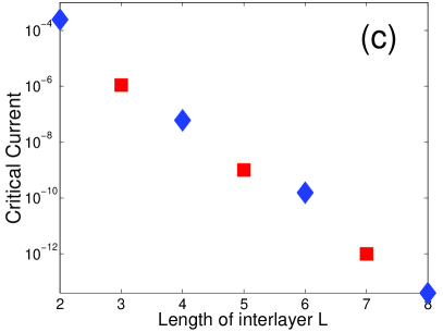
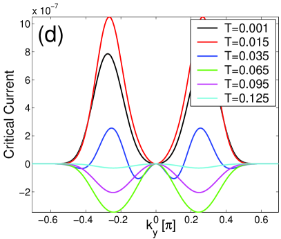
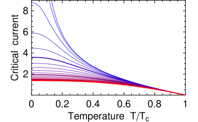
For /AF/ junctions, the behavior as a function of interlayer thickness exists both for 100 and 110 orientationsandersen06 . This is not the case for /AF/ junctions, where the 100 case displays only 0-junction characteristics with an Ambegaokar-Baratoff like dependence of . Therefore, we focus on the more interesting 110 oriented /AF/ junctions. We discuss only identical (and identically oriented) junctions, and restrict ourselves to the tunnelling limit where the current-phase relation is sinusoidal, and . The 110 oriented /AF/ junctions are categorized further into d/AFeven/d and d/AFodd/d junctions depending on whether the interlayer consists of an even or odd number of chains, respectively. In Fig. 1(a) and 1(b) we show typical self-consistent results for as a function of for even and odd interlayer-chains, respectively. As seen from Fig. 1(a), d/AFeven/d are 0-junctions with a -like dependence of in the large- limit. The small dip in at low is caused by the finite width of the interlayer and disappears in the limits . As shown in Fig. 1(b), in 110 d/AFodd/d junctions exhibits a surprisingly rich dependence: as is increased, the pure 0-junction at low becomes a -junction at high , crossing over to 0-junction behavior at some which eventually vanishes in the large- limit where . The systematic -junction oscillations versus interlayer thickness is shown in Fig. 1(c). The -resolved current corresponding to parameters similar to the green curve in Fig. 1(b), is shown in Fig. 1(d). The same momentum region contributes to the current at all , a fact which will ease the analytical interpretation presented in the next section. Results qualitatively similar to those shown in Fig. 1 can be also obtained for thicker junctions with smaller values of .
We now study /AF/ junctions within a quasiclassical approach where, as usual, all characteristic energies are assumed to be much less than the Fermi energy . We assume for the coherence length , and the junction properties are conveniently expressed in terms of the scattering matrix containing the reflection and transmission amplitudes. The Josephson current is carried entirely by phase-dependent Andreev bound states.
For the 100 orientation the -wave order parameter does not change its sign in specular reflection, but it changes sign in Q-reflection processes. By contrast, in the 110 case the -wave order parameter changes its sign both in specular and in Q-reflection events. An important manifestation of this physical difference between effects of Q-reflection for different AF-interface orientations is that the transition does not take place for 100 orientation in -wave junctions, but the transition is, in general, present in 110 -wave, as well as 100 -wave junctions. More formally, in the 110 case the specular and Q-reflection possess identical outgoing group velocities and form the outgoing flow along one and the same direction. This permits the reduction of the problem to a standard situation with conventional number of incoming and outgoing waves, which determines the rank of the S-matrix. This is not the case for the 100 orientation, when specular and Q reflection should be considered separately. This increases the rank of the S-matrix and makes ultimate results for 100 junctions with finite transparencies strongly different compared to the 110 case. In the following we focus solely on the 110 orientated interfaces.
For d/AFodd/d junctions, the general structure of the matrix is similar to that of d/F/d junctions with symmetric F interfaces. This follows from the fact that in the (110) orientation and for an odd number of chains in the interlayer, all spins are aligned in the outermost chains. For (110) d/AFeven/d junctions, the outermost chains of the AF interface have opposite spin polarizations (but still all aligned within each chain) and the matrix is isomorphic to the three-layer FIF interface with antiparallel orientations of the two F layersbbk02 . The existence of the even-odd () behavior shown in Fig. 1(c) follows directly from this link between the matrices for 110 /AF/ and d/F/d junctionsandersen06 . However, in order to understand the dependence of and obtain quantitative criteria for transitions between 0- or -junction behavior, we turn now to the explicit calculations.
Consider first (110) d/AFeven/d junctions where the transparency coefficients satisfy , resulting in the following Josephson current
| (3) |
where , and is the phase difference across the junction. Here, not only and , but also the spin-mixing parameter (), are all -dependent, and the total current is a sum of Eq.(3) over all values of andersen06 . However, as seen from Fig. 1(d), the -sum is unimportant for understanding the qualitative behavior. Eq. (3) is valid for arbitrary transparency, and the critical current is plotted in Fig. 2(left) for a range of . In agreement with Fig. 1(a), the junction is always a 0-junction. Near , Eq. (3) reduces to which coincides with the result in nonmagnetic (110) symmetric /I/ junctions. However, at low the current (3) is given by which, in the tunnelling limit, reduces to . Therefore, due to the factor , we find the remarkable result that the current substantially exceeds the critical current in nonmagnetic (110) /I/ junctions with the same transparency coefficient (Fig. 2).
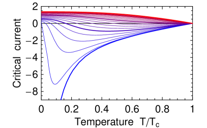
Next we discuss the dependence of for 110 d/AFodd/d junctions. As argued above, this junction is similar to 110 d/F/d junctions with symmetric F interlayer. In the tunnelling limit we obtain the following expression for ()
| (4) | |||||
which is plotted in Fig. 2(right) for (see below). The result for an arbitrary transparency can be obtained along similar lines to Ref. bb02, . In the absence of magnetism, when , , and for zero transparency , there are zero-energy Andreev bound states at both /I surfaces of the (110) /I/ junction. With increasing , the mid-gap states on each /I surface evolve into spin-split Andreev states on a /FI surface. For a given , the energies of these spin-split states are . This is different from the -wave case where fogel00 , and therefore the behavior of the Josephson current in s/F/s tunnel junctionsbb02 strongly differs from -wave magnetic junctions. Eq.(4) can be qualitatively understood as follows: in tunnel junctions the surface states further split and become phase-dependent due to a finite transparency. As a result, four current-carrying interface Andreev states exist for a given . Eq. (4) represents the Josephson current carried by these states in the tunnelling limit, when two spin-split surface states on each side of the junction only slightly overlap through the interlayer.
In the limit of a nonmagnetic interlayer (, ), only the second term in Eq.(4) survives and one obtains , with the well-known -behavior for /I/ junctions. This result is the tunnelling limit of the more general current-phase relationriedel ; tanakakas2000
| (5) |
Hence, there are no transitions in (110) -wave nonmagnetic junctions. This, however, is not the case, in the presence of magnetic interlayers with finite spin-mixing . Finite values of result in the appearance of the additional (first) term in Eq.(4), which is comparatively small for small , and for has the opposite sign compared to the second term. The second term in Eq.(4) is, in its turn, strongly modified due to finite at sufficiently low . Indeed, it becomes exponentially small, if is much less than the spin-split finite energies of the Andreev states . At the same time, the second term in Eq.(4) dominates the current at higher , for example, near . For this reason the transition arises in magnetic 110 d/AFodd/d tunnel junctions under the condition , as a result of the interplay of the two terms with opposite signs in Eq.(4). In principle, the change of sign of the total current in (4) takes place with varying for any small value of , but effects of finite transparency confine the conditions for the presence of a transition to not too small values of .
For deriving the conditions for the presence of the transition in the tunnelling limit, it is convenient to consider two limiting cases of Eq.(4), one near and another at low . Under the condition , Eq.(4) reduces to the simple expression
| (6) |
which is suppressed by the factor compared to the corresponding nonmagnetic /I/ junction. Eq. (6) is valid, in particular, near . Under the opposite condition , Eq.(4) becomes
| (7) |
which is suppressed by the factor compared to nonmagnetic /I/ junction. Comparing signs of Eqs. (6) and (7), it is evident that the transition takes place with varying when , that is for . For (which is the case for d/AFodd/d junctions) and the -state is the ground state of the junction, whereas the -state exists near in qualitative agreement with Fig. 1(b). Note that transitions in s/F/s junctions happens when the opposite inequality is satisfiedbb02 . We stress that our results (4), (6) and (7) describe also the current in d/F/d junctions.
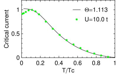
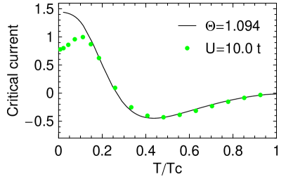
Above we have extracted the form of the current characteristics in d/AF/d junctions via both numerical BdG methods and an analytical quasiclassical approach. An obvious question is how well these two methods agree. To this end, in Fig. 3 we plot again the BdG results (normalized to 1.0) for the case with (left) and (right), and show self-consistent quasiclassical fits to these curves. Here and the special choice has been taken. The transparency has been adjusted to fit the BdG data. As seen, there is overall very good agreement. At low some discrepancy can be detected, which we believe originates from the finite interlayer thickness used in the BdG calculations and/or the different bandstructures (circular vs square Fermi surface in the quasiclassical and BdG approach, respectively). Disregarding any explicit dependence of the transparency coefficients and the parameter in the quasiclassical calculations may also play a role.
Experimental detection of transitions in /AF/ junctions may be possible in sandwich structures of high-doped and un-doped high- materials similar to what was constructed for c-axis junctionsbozovic . Recently, Oh et al.oh:2005 , invented a spatially controlled doping method and fabricated in-plane 100 /AF/ junctions. Our results show that the fabrication of similar 110 junctions and a detailed study of their Josephson current characteristics holds the promise of several unusual properties as shown in Figs. 1-2. Realistic junctions will contain regions with varying interlayer thickness, but if these are sufficiently few, the regions with shortest thickness should dominate the current. Alternatively, one needs to average the current over interface imperfections. in even junctions dominates at low only in the limit of large . Then we have a small and 0-junction with a low- anomaly in . Otherwise critical currents in even and odd junctions are of the same order. For (i.e. ) the currents have identical signs at all (0-junctions). For , the -junction state arises in odd junctions near , resulting in an overall cancellation of odd and even contributions to the current.
IV Grain boundary junctions
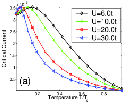
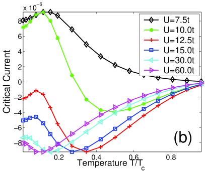
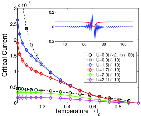
Finally, we turn to the question of through grain boundaries, where a strong discrepancy between theory and experiment has been known for some time: when the GB is modeled as a /I/ junction the zero-energy state existing in the 110 orientation results in a large low increase of as compared to the 100 orientation (see dashed lines in Fig. 4). However, the opposite behavior is obtained in experiments: is largest for 100 orientations and drops exponentially with increased angle between the GB and the crystal axishilgenkamp02 . We model the GB using Eq.(1) in a /I/ geometry with a potential inside the insulating layer (I) and in the leads only. For sufficiently small , magnetization is absent in the superconducting leads, but the magnetic correlations can lead to instabilities near interfaces that suppress the dSC order parameterOhashi99 ; honerkamp:2000 , as shown in the inset of Fig. 4. The main body of Fig. 4 shows for a range of all small enough not to induce magnetization in the bulk. Contrary to the 100 orientation, through 110 GB can be significantly reduced by surface-induced magnetic order for , where is the critical temperature for the surface magnetization. In fact, as seen from Fig. 4 there exists a range of where at low becomes smaller in the 110 orientation compared to the 100. This shows the importance of competing surface effects even though a complete understanding of the physics of GB junctions requires more detailed microscopic calculations.
V Conclusions
We have studied the dc Josephson current through d/AF/d tunnel junctions as a function of interlayer thickness and temperature using both numerical BdG diagonalization and analytical quasiclassical methods. For an odd (even) number of antiferromagnetic chains in the interlayer, the current characteristics of 110 oriented interfaces display ()-junction behavior. In addition d/AFodd/d junctions can exhibit transitions as a function of temperature. We have shown that in terms of the spin-mixing parameter , the condition for the latter is given by . This is the opposite regime as compared to leads with -wave pairing symmetry where temperature-induced transitions take place for . Another important difference between s/AF/s and d/AF/d junctions exists for the 100 orientation, where -wave junctions always are 0-junctions whereas this is not the case for -wave superconductors. Finally we studied grain boundary junctions modeled as d/I/d junctions but with subdominant magnetic correlations in the superconducting leads allowing for interface-induced magnetism near grains which tend to suppress the -wave order parameter. We showed that this mechanism can lead to larger critical currents for the 100 orientation than for 110, in qualitative agreement with experiments.
VI Acknowledgements
Partial support for this research was provided by DOE Grant DE-FG02-05ER46236. Yu. S. B. acknowledges the support of RFBR grant 05-02-17175. Numerical calculations were performed at the University of Florida High-Performance Computing Center (http://hpc.ufl.edu).
References
- (1) A. I. Buzdin, Rev. Mod. Phys. 77, 935 (2005).
- (2) V. V. Ryazanov, V. A. Oboznov, A. Yu. Rusanov, A. V. Veretennikov, A. A. Golubov, and J. Aarts, Phys. Rev. Lett. 86, 2427 (2001).
- (3) T. Kontos, M. Aprili, J. Lesueur, F. Genêt, B. Stephanidis, and R. Boursier, Phys. Rev. Lett. 89, 137007 (2002).
- (4) L. N. Bulaevskii, V. V. Kuzii, and A. A. Sobyanin, JETP Lett. 25, 290 (1977).
- (5) E. Terzioglu and M. R. Beasley, IEEE Trans. Appl. Supercond. 8, 48 (1998).
- (6) I. Zutić, J. Fabian, and S. Das Sarma, Rev. Mod. Phys. 76, 323 (2004).
- (7) I. V. Bobkova, P. J. Hirschfeld, and Yu. S. Barash, Phys. Rev. Lett. 94, 037005 (2005).
- (8) B. M. Andersen, I. V. Bobkova, P. J. Hirschfeld, and Yu. S. Barash, Phys. Rev. B 72, 184510 (2005).
- (9) B. M. Andersen, I. V. Bobkova, P. J. Hirschfeld, and Yu. S. Barash, Phys. Rev. Lett. 96, 117005 (2006).
- (10) Yu.S. Barash, H. Burkhardt, and D. Rainer, Phys. Rev. Lett. 77, 4070 (1996).
- (11) Y. Tanaka and S. Kashiwaya, Phys. Rev. B 53, R11957 (1996).
- (12) E. Il’ichev, M. Grajcar, R. Hlubina, R. P. J. IJsselsteijn, H. E. Hoenig, H.-G. Meyer, A. Golubov, M. H. S. Amin, A. M. Zagoskin, A. N. Omelyanchuk, and M. Yu. Kupriyanov, Phys. Rev. Lett. 86, 5369 (2001).
- (13) G. Testa, A. Monaco, E. Esposito, E. Sarnelli, D.-J. Kang, S. H. Mennema, E. J. Tarte, and M. G. Blamire, Appl. Phys. Lett. 85, 1202 (2004).
- (14) G. Testa, E. Sarnelli, A. Monaco, E. Esposito, M. Ejrnaes, D.-J. Kang, S. H. Mennema, E. J. Tarte, and M. G. Blamire, Phys. Rev. B 71, 134520 (2005).
- (15) Yu. S. Barash, I. V. Bobkova, and T. Kopp, Phys. Rev. B 66, 140503(R) (2002).
- (16) Yu. S. Barash and I. V. Bobkova, Phys. Rev. B 65, 144502 (2002).
- (17) M. Fogelström, Phys. Rev. B 62, 11812 (2000).
- (18) R. A. Riedel and P. F. Bagwell, Phys. Rev. B 57, 6084 (1998).
- (19) Y. Tanaka and S. Kashiwaya, Rep. Prog. Phys. 63, 1641 (2000).
- (20) I. Bozovic, G. Logvenov, M. A. J. Verhoeven, P. Caputo, E. Goldobin, and T. H. Geballe, Nature 422, 873 (2003).
- (21) S. Oh, J. A. Bonetti, K. Inderhees, D. J. Van Harlingen, and J. N. Eckstein, Appl. Phys. Lett. 87, 231911 (2005).
- (22) H. Hilgenkamp and J. Mannhart, Rev. Mod. Phys. 74, 485 (2002).
- (23) Y. Ohashi, Phys. Rev. B 60, 15388 (1999).
- (24) C. Honerkamp, K. Wakabayashi, and M. Sigrist, Europhys. Lett. 50, 368 (2000).