Present address:]Zentralabteilung Technologie, FZ Jülich GmbH, D-52425 Jülich, Germany
Formation of Hydrogen Impurity States in Silicon and Insulators at Low Implantation Energies
Abstract
The formation of hydrogen-like muonium (Mu) has been studied as a function of implantation energy in intrinsic Si, thin films of condensed van der Waals gases (N2, Ne, Ar, Xe), fused and crystalline quartz and sapphire. By varying the initial energy of positive muons () between 1 and 30 keV the number of electron-hole pairs generated in the ionization track of the can be tuned between a few and several thousand. The results show the strong suppression of the formation of those Mu states that depend on the availability of excess electrons. This indicates, that the role of H-impurity states in determining electric properties of semiconductors and insulators depends on the way how atomic H is introduced into the material.
pacs:
78.70.-g, 76.75.+i, 36.10.DrThe implantation of energetic (MeV) positive muons () in insulators or semiconductors commonly leads to the formation of the hydrogen-like bound state muonium [Mu )] with a final charge state which can be either positive (Mu+), neutral (Mu0), or negative (Mu-). In semiconductors Mu is used to identify and investigate the electronic properties and the behavior of isolated hydrogen-like states patt1988rmp ; chow1998 ; cox2003JPCondMatt , and hydrogen-related impurities which are of fundamental and technological interest due to their influence on the electrical and optical properties. Isolated H atoms in materials are difficult to detect by other spectroscopic means, which mostly require high H concentrations (see pereira2005prb ; luepke2002prl and references therein for examples of vibrational spectroscopy studies of Si). In contrast, Mu – which behaves like a light H isotope () – can be easily detected and characterized by the muon spin rotation (SR) technique due to its high sensitivity per spin. Muonium states, formed after implantation of energetic , remain isolated during the observational time window of the order of the life time (2.2 s). Therefore, a large amount of experimental information on the formation, structure and electrical activity of isolated H states in semiconductors has been obtained from SR, which has played a pioneering role in the identification and characterization of hydrogen-like states. In Si, Ge and semiconductors of the III-V family two Mu states lying deep in the band gap have been identified at low temperatures ( K)patt1988rmp : normal MuT in the tetrahedral interstitial site with a large isotropic hyperfine interaction (hfi), and anomalous MuBC at a bond-center between two host atoms with a smaller, anisotropic hfi. In covalent semiconductors, MuT acts as an acceptor and MuBC as a donor. Recently, novel, very weakly bound Mu states (shallow Mu, binding energies 15 - 60 meV) with very low hfi have been established in a number of II-VI and III-V (nitrides) compounds gil2001prb ; cox2001prl ; davies2003apl . Theoretical work has shown an universal alignment of hydrogen levels in semiconductors and insulators vdWalle2003nature , from which the electronic properties of hydrogen impurities can be derived. The predicted shallow donor hydrogen states in InN and ZnO have been confirmed experimentally by SR davies2003apl ; cox2001prl .
However, it has to be kept in mind that by the techniques used so far the spectroscopically investigated H-isotopes are energetically inserted in the solid. This results in a large number of electron-hole pairs generated during slowing down of the incident particle. For instance, all SR experiments performed up to now used MeV- beams that generate – electron-hole pairs per implanted in the ionization track Neh . Similar or higher numbers of excess are created by the implantation of H or D ions used in the case of vibrational spectroscopy or channeling experiments. A sizable fraction of these electron-hole pairs escapes prompt recombination and is still present around the thermalized impurity as shown in SR experiments with applied electric field E of both polarities. The E-field clearly changes the Mu formation probability by pushing track and apart or together kra1992prl ; sto1997prl ; dge1999pla ; dge2002prb , demonstrating that a significant fraction of Mu in semiconductors and insulators is generated by the capture of a track after the has stopped at an interstitial or bond site. In semiconductors it appears that this so-called delayed Mu formation (in contrast to prompt Mu, where Mu forms during slowing down in charge-exchange cycles, followed by thermalization of Mu due to elastic collisions dge2002prb ) is the origin of MuBC and for the recently discovered shallow Mu centers in III-V and II-VI semiconductors sto1997prl ; dge1999pla ; dge2003prb . The question therefore arises, whether and how the final states are influenced by the formation process, which is essential for studies on technologically important semiconductors and insulators. This can be studied by using the polarized low-energy (LE-) beam at the Paul Scherrer Insitute (PSI, Villigen, Switzerland) em1994prl ; em2003pb with variable implantation energy between 1 and 30 keV. It allows to investigate the formation of hydrogen-like Mu impurity states as a function of energy, i.e. as a function of . By varying the energy, can be tuned between a few and several thousand. This is up to five orders of magnitude less than for conventional MeV-muon beams. Below 1 keV nearly no track products are generated, thus approximating the case where H impurities are thermally introduced, which is the way, how trace atoms are incorporated in the lattice in the course of wafer growth and fabrication processes.
In this Letter we investigate for the first time the formation of thermal Mu as a prototype for isolated H impurities as a function of implantation energy. In addition to intrinsic Si and sapphire (Al2O3) with more than one type of Mu we investigated thin films of van der Waals solids (s-Ne, s-Ar, s-Xe, s-N2) and fused and crystalline quartz (SiO2) due to their simplicity concerning the final charge states: only one type of Mu0 exists with an isotropic hfi close to vacuum Mu0. We find that delayed Mu formation is energy dependent in the keV range in all the investigated samples. Below 10 keV the formation of those H impurity states that require a sizeable amount of excess is strongly suppressed. The data on Si and Al2O3 support the interpretations that Mu in Si sto1997prl and Mu- in Al2O3 brewer-jd2000 are formed by delayed capture of a track .
The SR technique allows to differentiate between paramagnetic (Mu0) and in diamagnetic environment (free , Mu+ or Mu-). Due to the hyperfine coupling between the and the spin the observable Larmor precession frequency of isotropic Mu0 is about 103 times larger than for the free . It splits into two intra-triplet lines that merge to one line at low fields ( mT) where 50% of the muon polarization is not observed due to unresolved hyperfine oscillations between the triplet and singlet state. The diamagnetic and paramagnetic decay asymmetries and were determined by measuring the amplitudes of the and Mu precession signals in transverse (perpendicular to the spin) magnetic field, applied parallel to the sample normal. and are proportional to the fraction of muons in that particular states.
The 0.5-mm thick Si sample with 50 mm diameter (undoped, resistivity 10 kcm, capped by a 2-nm thick oxide layer) was oriented with the direction parallel to the sample normal. The quartz disc samples had thicknesses of 1 and 2 mm [SiO2 crystal and fused quartz (Suprasil), respectively] and 50 mm diameter. The Al2O3 sample was a 0.5 mm-thick single crystal with 60 mm diameter. The solid gas films were grown at partial pressures between and hPa. Film thicknesses were about 1000 nm which is sufficient to stop all LE- in the layer. At these deposition pressures grain sizes of order 100 nm are obtained rgs1975 . For details on the experimental setup we refer to ref. tp2003pb .
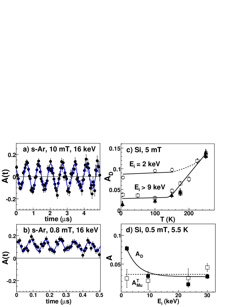
Figure 1 shows typical SR asymmetry spectra, and displays the results for Si. In Si, at 5 mT only the precession of the diamagnetic signal is observed. Due to limited statistics and time resolution Mu precession frequencies MHz are too high to be resolved with our present setup. In a field of 5 mT, the Mu intra-triplet lines are at about 70 MHz, whereas the Mu transitions are between 35 and 50 MHz, depending on the orientation of the B-field with respect to the crystal axis. At 0.5 mT the Mu frequencies are nearly unchanged and therefore not observable with our setup, whereas the 7-MHz signal of Mu becomes visible. The 0.5-mT data are fitted with two components, a precession signal and the Mu signal with exponential relaxation, whereas the 5-mT data are fitted with the precession signal only. The temperature dependence of at different implantation energies is shown in Fig. 1a). Above 9 keV - corresponding to a mean implantation depth of 65 nm and Neh - exhibits the same temperature behavior as in bulk SR experiments sto1997prl . The increase of above 150 K reflects the thermally induced ionization of Mu. At keV ( nm) and K is significantly larger than at higher energies. As Fig. 1b) shows the behavior of is not related to a change of the Mu fraction, which contrary to does not depend on . It rather reflects the unobserved Mu fraction which decreases with decreasing energy and number of available track . This is also supported by the convergence of the two curves in Fig. 1a) at high where Mu is ionized. The -nm thick oxide layer present on the Si surface is too thin to explain the observed reduction of the Mu formation. Moreover, in a SiO2 layer at low energy a higher Mu fraction should be observed, see Fig. 2b). The different dependence on the availability of excess indicate that the main fraction of Mu is due to delayed formation, whereas Mu is a consequence of charge-exchange processes at epithermal energies – in agreement with bulk SR studies, where an applied E-field was used to vary the average distance between and excess , and therefore the relative formation probability of these two states sto1997prl .
Figure 2 shows the energy dependence of and for s-Ar (a) and SiO2 (b). Only isotropic Mu is present, and and represent a direct measure of the and Mu fraction in the sample. The sum = = 0.263(1) is the total observable asymmetry, and there is within the experimental errors no missing fraction. Qualitatively, the s-Ar and SiO2 data display the same behavior: with increasing energy is decreasing while is increasing correspondingly.

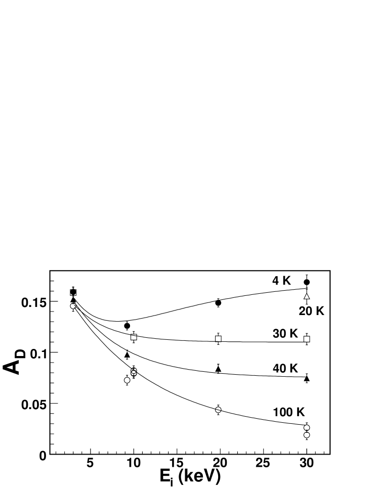
The energy-dependent diamagnetic fractions for various insulators are summarized in Fig. 3. With the exception of s-Ne all samples show a decreasing diamagnetic fraction with increasing energy. For SiO2 and s-Xe bulk Mu fractions ) of 85% and %, respectively, are obtained at keV [corresponding to nm (SiO2), nm (s-Xe)]. At this energy the number of electron-hole pairs created in the ionization track is about 1000 Neh . In the s-Ar and s-N2 films even at the highest energy the observed Mu fractions () are lower than the bulk results obtained with 4-MeV [ (s-Ar), (s-N2 at K)]. The discrepancy is even more drastic for s-Ne where the film data are consistent with in contrast to the bulk data with dge2002prb .

This disagreement can be explained by the suppression of Mu formation in granular s-Ne, s-Ar and s-N2 thin films, as we discuss below.
The decrease of with increasing reflects the onset of delayed Mu formation with increasing availability of excess . From the flattening of at keV we estimate the number of excess necessary to saturate the delayed Mu yield to be of the order of thousand. The may escape recombination with the by several processes: recombination with a cation from the ion track, trapping at grain boundaries, voids, and surfaces or escape from the surface ( escape depth nm in s-Ar and s-Xe bar1998prb , mean free path in Si is nm at 300 K, increasing to nm at lower ). An additional obstacle for electron-muon recombination is also the large escape depth of 20 - 100 nm of epithermal in wide band gap insulators such as s-N2, s-Ar and s-Ne em2004JPCondMatt : after leaving the charge-exchange cycles where the last are released the may move such a distance away from its ionization track, further losing energy inefficiently by elastic collisions. This large separation and the trapping of combine all together to suppress the delayed Mu formation channel in s-Ne, s-Ar and s-N2. The total suppression of Mu formation in s-Ne is probably a consequence of a escape depth larger than the typical grain size, making the formation of a delayed bound state unlikely.
The energy dependence at K of in sapphire (Fig. 4) shows an interesting anomaly compared to the data presented so far. At 100 K decreases with increasing energy and reaches its smallest value of 0.025 at 30 keV. This behavior correlates with the onset of delayed formation of Mu0 as seen in other insulators. The energy dependence of becomes less pronounced on reducing the temperature. At 4 K exhibits a minimum at 10 keV and starts to increase again when further increasing the energy. This may reflect the delayed formation of diamagnetic Mu-, as suggested in a previous E-field SR experiment where the disappearence of Mu- with increasing is interpreted as thermal ioniziation of Mu- with an activation temperature of 130 K brewer-jd2000 . A recent theoretical work shows that H- could be the stable charge state in Al2O3 peacock2003 . Our data support this idea, and that Mu- is formed by delayed capture.
In conclusion, the measured energy dependence of Mu formation in intrinsic Si and insulators shows as a general behavior that the formation of delayed Mu states requires the presence of the order of thousand excess in the ionization track. With LE- H-impurity states can be studied without the generation of a non-equilibrium electron track. From the implantation energies involved we infer that the length scale of that part of the track that is involved in delayed Mu formation is of the order of 100 nm. At energies 3 keV delayed Mu formation is nearly absent. This indicates that the formation of those H-impurity states which heavily depend on the availability of excess is strongly suppressed in cases where the H-isotope is inserted in the solid without the concomitant presence of a sizeable number of excess . This implies, that the role of H-impurity states in determining electric properties of semiconductors and insulators depends on the way how atomic H is incorporated into the material. The question of the relative importance of different possible H-states and their occurrence as native impurity states in semiconductors and insulators is generally not addressed and we hope that our results will foster new theoretical and experimental studies in this area.
We are extending this kind of experiments to the investigation of shallow Mu states: Preliminary data in ZnO show also a decreasing shallow Mu fraction with decreasing implantation energy, which further supports the general trend found in other materials.
This work was fully performed at the Swiss Muon Source SS, Paul Scherrer Institute, Villigen, Switzerland. We are grateful to S.F.J. Cox for valuable discussions. We thank C. David from LMN at PSI for providing the Si sample. We thank M. Birke, Ch. Niedermayer and M. Pleines for their help in the initial phase of the experiment. The technical support by H.P. Weber is gratefully acknowledged.
References
- (1) B. D. Patterson, Rev. Mod. Phys. 60, 69 (1988).
- (2) K. H. Chow, B. Hitti, and R. F. Kiefl, in Semiconductors and Semimetals Vol. 51A, edited by M. Stavola (Academic Press, San Diego and London, 1998).
- (3) S. F. J. Cox, J. Phys.: Cond. Matt. 15, R1727 (2003).
- (4) R. N. Pereira et al., Phys. Rev. B 72, 115212 (2005).
- (5) G. Lüpke et al., Phys. Rev. Lett. 88, 135501 (2002).
- (6) J. M. Gil et al., Phys. Rev. B 64, 075205 (2001).
- (7) S. F. J. Cox et al., Phys. Rev. Lett. 86, 2601 (2001).
- (8) E. A. Davis, S. F. J. Cox, R. L. Lichti, and C. G. V. de Walle, Appl. Phys. Lett. 82, 592 (2003).
- (9) C. G. Van de Walle and J. Neugebauer, Nature 423, 626 (2003).
- (10) For the investigated insulators the mean energy for electron-hole pair creation ranges from 18 eV (SiO2) to 40 eV for Ne (p. 1136 Vol 2 of rgs1975 ). For Si, 3.7 eV [F. E. Emery and T. A. Rabson, Phys. Rev. 140, A2089 (1965)].
- (11) E. Krasnoperov et al., Phys. Rev. Lett. 69, 1560 (1992).
- (12) V. Storchak et al., Phys. Rev. Lett. 78, 2835 (1997).
- (13) D. G. Eshchenko, V. Storchak, and G. D. Morris, Phys. Lett. A 264, 226 (1999).
- (14) D. G. Eshchenko et al., Phys. Rev. B 66, 035105 (2002).
- (15) D. G. Eshchenko, V. G. Storchak, S. P. Cottrell, and S. F. J. Cox, Phys. Rev. B 68, 073201 (2003).
- (16) E. Morenzoni et al., Phys. Rev. Lett. 72, 2793 (1994).
- (17) E. Morenzoni et al., Physica B 326, 196 (2003).
- (18) J. D. Brewer et al., Physica B 289-290, 428 (2000).
- (19) Rare gas solids, Vol.I and II, edited by M. L. Klein and J. A. Venables (Academic, New York, 1975).
- (20) T. Prokscha et al., Physica B 326, 52 (2003).
- (21) R. A. Baragiola, M. Shi, R. A. Vidal, and C. A. Dukes, Phys. Rev. B 58, 13212 (1998).
- (22) E. Morenzoni et al., J. Phys.: Cond. Matt. 16, S4583 (2004).
- (23) P. W. Peakcock and J. Robertson, Appl. Phys. Lett. 83, 2025 (2003).