Measurement of the spin polarization of the magnetic semiconductor EuS with zero-field and Zeeman-split Andreev reflection spectroscopy
Abstract
We report measurements of the spin polarization (P) of the concentrated magnetic semiconductor EuS using both zero-field and Zeeman-split Andreev reflection spectroscopy (ARS) with EuS/Al planar junctions. The zero-field ARS spectra are well described by the modified (spin-polarized) BTK model with expected superconducting energy gap and actual measurement temperature (no additional spectral broadening). The fittings consistently yield P close to 80% regardless of the barrier strength. Moreover, we performed ARS in the presence of a Zeeman-splitting of the quasiparticle density of states in Al. To describe the Zeeman-split ARS spectra, we develop a theoretical model which incorporates the solution to the Maki-Fulde equations into the modified BTK analysis. The method enables the determination of the magnitude as well as the sign of P with ARS, and the results are consistent with those from the zero-field ARS. The experiments extend the utility of field-split superconducting spectroscopy from tunnel junctions to Andreev junctions of arbitrary barrier strengths.
pacs:
72.25.Dc, 72.25.Mk, 74.45.+cSuperconducting spectroscopy has been one of the most effective means of determining the spin polarization (P) of itinerant charge carriers in ferromagnetic materials. Two types of electron transport in a superconductor (S)/ferromagnet (Fm) junction can be used for this purpose: single particle tunneling a1 and Andreev reflection (AR) a2 . AR a3 , which occurs at an S/normal-metal (N) interface, is a process that converts the quasiparticle current in N into supercurrent in S. In AR an incident electron from the N side pairs up with an electron of opposite spin and momentum to form a Cooper pair in order to enter the S, and a hole is retro-reflected to conserve charge, spin, and momentum. Therefore, AR results in a doubling of charge transfer across the junction and an enhancement of the subgap junction conductance. In an S/Fm junction, AR is suppressed due to the spin imbalance near the Fermi level and the resulting reduction of the subgap Andreev conductance can in principle be used to infer P a4 . In practice, in most cases both AR and normal reflections are present and the zero-bias conductance alone does not give a reliable measure of P; one needs to measure and analyze the entire conductance spectrum in order to separate the effects of spin polarization and single electron tunneling, and reliably determine P. The analysis of the conductance spectrum is done with a modified version of the Blonder-Tinkham-Klapwijk (BTK) theory a5 , which takes account of the spin polarization in the ferromagnet and computes the junction conductance with a two-current (spin polarized and unpolarized) model a6 ; a7 ; a8 . In the BTK theory the probability of AR and normal reflection is determined by the barrier strength, described by a dimensionless parameter , which includes effects of physical scattering as well as band structure mismatches. AR spectroscopy (ARS) has been widely implemented in point contact setups a4 ; a8 , which has become an efficient technique for rapid measurement of P for a large variety of ferromagnetic materials in various forms. However, there remain several limitations and controversial issues with point contact ARS. First, a point contact typically does not represent an interface in a realistic device structure, while the magnitude and even the sign of P is known to depend on the nature of the interface a9 . ARS, in general, only measures the magnitude of P and cannot determine its sign. Furthermore, the fitting of the point contact ARS often requires an artificially large spectral broadening a10 (or equivalently, the use of a temperature in the Fermi function much greater than the actual measurement temperature), and sometimes superconducting gaps much different from the expected values a8 ; a10 . Finally, there are ubiquitous observations of a precipitous decline of measured P with increasing in a variety of systems a8 ; a10 ; a11 ; a12 , which remain unexplained.
Single-particle tunneling in zero field cannot be used to measure P because of the degeneracy of the spin-up and spin-down electrons. However, the application of an external magnetic field lifts this degeneracy and the resulting asymmetry in the conductance spectrum can be utilized to calculate the magnitude and determine the sign of P a1 . Quantitative fits to the tunneling conductance spectrum with complex structures are realized by using the coupled spin-up and spin-down superconducting density of states (DOS) derived from the solution to the Maki-Fulde equations a13 , which produces highly reliable and unique P values a14 ; a15 . Technically, such spin-polarized tunneling (SPT) experiments are more challenging to implement compared to ARS since they require fabrication of high-quality tunnel junctions and a superconducting electrode with high critical field and small spin-orbit coupling, which is in practice limited to an ultrathin Al film.
In this paper, we report on the zero-field and Zeeman-split ARS measurements of a series of doped-EuS/Al planar junctions. By controlling the growth temperature, the EuS films were naturally doped to different levels due to varying degree of sulfur vacancies a16 , which enabled realization of junctions of a relatively wide range of intermediate values where both AR and single electron tunneling are prominent. We observe that the conductance spectra can be fit straightforwardly (with zero additional spectral broadening and expected gap values) to the spin-polarized BTK model. The fittings consistently yield P of 80 % regardless of the values. Moreover, by using planar junctions and thin Al counter-electrode, we are able to obtain the ARS spectra in a large magnetic field. The Zeeman-split ARS experiments have provided a means to extract the sign of P from ARS. It also demonstrates that the field-splitting of the conductance spectra is not limited to tunnel junctions but can be applied to S/Fm junctions of arbitrary barrier strengths, greatly simplifying its implementation. These experiments have provided a reliable determination of the magnitude (80 %) and sign (+, majority spin polarized) of P for the doped EuS films.
EuS is a prototypical concentrated magnetic semiconductor. One of the most attractive features found in such materials is a strong exchange interaction between the spins of the itinerant charge carriers in the conduction band and the localized magnetic moments. This interaction is manifested as a giant spontaneous band splitting of 0.5 eV a17 . Such materials offer high magnetization and wide range of conductivity tunability so that they can be used as spin filters a18 ; a19 in the insulating state and as spin injectors when doped a20 ; a21 ; a22 . Thus they offer an ideal system to demonstrate the physics of semiconductor-based spintronic devices in proof-of-concept studies.
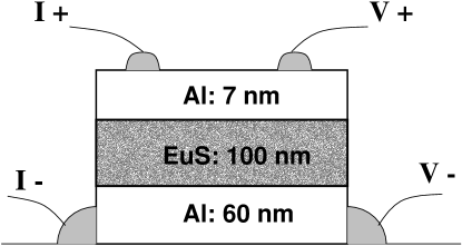
Doped-EuS/Al planar junctions were fabricated by vacuum deposition on insulating Si(100) or glass (Corning) substrates. A schematic diagram of the junction structure is shown in Figure 1. A relatively thick (50-60 nm) Al stripe was first deposited. Conducting EuS films of different conductivities, always 100 nm in thickness, were grown at various low substrate temperatures by electron beam evaporation in ultrahigh vacuum. The growth temperature was shown to be effective in producing EuS films of varying doping levels, from intrinsic to degenerate, by controlling the degree of sulfur deficiency a16 . Finally, a thin Al electrode, 7-8 nm in thickness, was thermally deposited immediately over the EuS as a cross-stripe defined by a shadow mask. The effective junction dimensions were mm2, and the junction resistances at liquid Helium temperature varied from 3 to 15 k. The conductance spectra were obtained in a 3He system using standard phase-sensitive lock-in detection. The EuS films used in the present study had low-temperature resistivity on the order of m cm and carrier density of cm-3; they served as conducting electrodes rather than insulating tunnel barriers. The bottom Al/EuS junction made in this fashion always resulted in a low-resistance Ohmic contact, which served to ensure that there was negligible current crowding in the top junction. A simple estimate of the resistance values shows that neither the EuS film nor the bottom contact contributes significantly to the measured resistance a23 . In addition, the application of a small parallel field of about 1 kG, which fully suppresses superconductivity in the thick bottom Al film but is much below the critical field of the thin top Al electrode (at least 1.8 T), had little effect on the conductance spectrum. This observation demonstrated unambiguously that the measured conductance spectra only reflected the top EuS/Al junction. The current ()-voltage () characteristics of the junction at temperatures above of Al shows a linear behavior. This is in stark contrast to EuS/In junctions, which show a highly nonlinear characteristic of a Schottky barrier a23 .
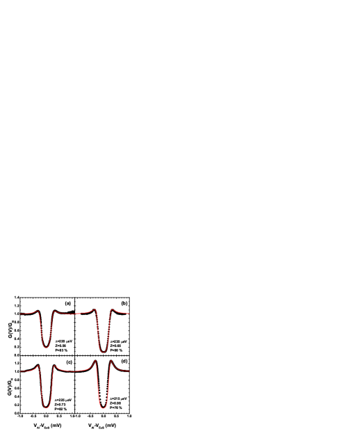
Shown in Figure 2 are the conductance spectra, d/d as a function of bias voltage , for four EuS/Al junctions of different barrier strengths in zero magnetic field. Each spectrum is normalized by the corresponding one at a magnetic field above the critical field for the Al. Qualitatively these spectra are consistent with those of a S/Fm Andreev junction of intermediate and large P for the Fm, as judged from the much diminished quasiparticle peaks near the superconducting energy gap, , and the low subgap conductance. These features are in contrast to the case of pure tunneling in EuS/In junctions where a Schottky barrier is present a23 . Quantitatively, these spectra can be analyzed within the spin-polarized BTK model. Excellent fits with physically sound parameters are obtained, as shown in Figure 2. We emphasize that the fitting is always performed in a straightforward manner and the only real adjustable fitting parameters are and P. Firstly, in all of the fits is always the actual measurement temperature; no additional spectral broadening, either in the form an artificial higher than the measurement temperature or an imaginary term in the electron energy a24 , is necessary to obtain good fits. This is evidence that Joule heating and inelastic effects including magnetic pairing-breaking are immeasurably small in these junctions. Secondly, the superconducting energy gaps for Al used are between 0.215 meV and 0.235 meV, values that are higher than that for bulk Al but expected of thin Al films a1 . The small variation in the gap value is most likely due to differences in the Al thickness. Thirdly, the P values resulting from these measurements and fittings show no substantial decline with increasing , as shown in Figure 3 in which we plot P from five such junctions as a function of . Within experimental uncertainty, there appears to be a small decrease of P with . However, this is in contrast to the results from point contact ARS in many systems where a much more significant decline of P ( %) with was observed in a similar range a11 . We attribute the small decrease in P in our data to actual changes of P in films grown at increasing substrate temperatures (from -2 ∘C to 120 ∘C), which is known to reduce the EuS film conductivity a16 . This result indicates that there is no intrinsic correlation between increase of spin-flip scattering and in these S/Fm junctions and a natural transition to the limit of SPT is possible. We point out that the above described observations, including the straightforward excellent agreement with the spin-polarized BTK model and the insensitivity of the determined P with , are not limited to the EuS junctions. Similar results have been observed by us in junctions with the half metal CrO2 a25 and the ferromagnetic semimetal EuB6 a26 .
In the BTK model, the parameter includes physical (elastic) scattering at the S/N interface as well as effects of band structure mismatches. For example, the Fermi velocity mismatch results in an effective barrier strength given by a27 , where is the ratio of the Fermi velocities of the ferromagnet and superconductor. Under the present growth conditions, it is estimated that the EuS has a carrier (electron) density of cm-3 at =4.5 K a16 . Assuming a parabolic band and a unitary effective electron mass, we estimate a Fermi velocity of m/s compared to m/s for the superconducting electrode Al. Such a large mismatch should result in a substantial even in the absence of any physical scattering at the interface. The small values in our junctions can be qualitatively attributed to enhanced junction transparency due to a high spin polarization in the Fm electrode a28 , which has been widely observed in different S/Fm junctions of high P a29 ; a25 ; a30 . Another outstanding issue in our data is the magnitude of the junction resistance, which is several orders of magnitude higher than the prediction of the BTK theory (for a ballistic point contact). The discrepancy has been widely observed in S/semiconductor (Sm) junctions of different materials and geometries a31 ; a32 ; a33 . Although a definitive explanation of this observation is still lacking, it is expected that the computation of the current and thus the junction resistance should depend on the junction geometry and be different in planar junctions a34 . It is important to note, however, that both in our junctions and other S/Sm structures a31 ; a32 ; a33 the conductance spectra are well described by the BTK theory. This represents a far more stringent requirement and strongly supports its applicability in these structures. This assertion is further reinforced by our results from measurements of the conductance spectra under Zeeman-splitting magnetic fields.

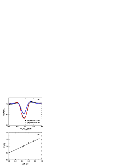
The use of a planar junction structure and thin Al electrodes afford us the opportunity to Zeeman-split the superconducting DOS and examine its consequences on the ARS spectrum. Figure 4(a) shows the conductance curves of the EuS/Al junction of Figure 2(a) at in-plane magnetic fields of 0.6 and 0.75 T. Because the Al electrode was on top of the EuS, it needed to be relatively thick (7-8 nm) which resulted in a relatively low critical field (2 T). However, even these relatively low magnetic fields induce a sizable shift of the conductance curve to the left. With the exception of noticeable asymmetry near the peaks, there are no observable additional features due to the minority spins. Qualitatively, these observations indicate a large, positive, P for the doped EuS. More importantly, to the best of our knowledge, this experiment represents the first study of Zeeman-split ARS in conventional S/Fm junctions.
In order to analyze the Zeeman-split ARS spectrum and independently extract P from the analysis, a thorough treatment of spin-polarized charge transport in an Andreev junction with Zeeman-splitting is necessary. This requires the use of the appropriate spin-resolved DOS for Al in a magnetic field when calculating the BTK transport (reflection and transmission) coefficients (Table II in Ref. 5). The BTK coefficients depend only on the parameter and the coherence factors:
| (1) |
where ) is the normalized BCS DOS
| (2) |
In a magnetic field is Zeeman-split and the BTK coefficients consequently become spin-dependent. Melin a35 assumed a simple Zeeman-splitting of the BCS DOS in an applied field and obtained the spin-dependent BTK coefficients using
| (3) |
where is the applied magnetic field. The Zeeman-split conductance curves at 0 K were then computed. This approach neglects the effects of spin-orbit coupling and depairing from the applied field. It has been shown a14 ; a15 that these effects are not negligible even in a material such as Al. They result in significant modification of the Zeeman-split conductance spectrum and, particularly, ambiguity in the determination of P from it. To obtain the DOS of a superconducting film in the presence of spin-orbit coupling (parameter ) and pair-breaking due to a magnetic field (parameter , which is proportional to ), one needs to solve the Maki-Fulde equations:
| (4) |
The solution of the coupled equations enables the determination of the spin-resolved superconducting DOS,
| (5) |
where are the spin up(down) superconducting DOS, is the normal state DOS of the superconductor at . The spin-up (down) DOS can then be used to calculate the corresponding spin-resolved BTK coefficients
| (6) |
where
| (7) |
We numerically solve the Maki-Fulde equations (Eq. 4) and obtain the actual DOS of the Al film in a magnetic field. The results are similar to those obtained in Ref. 14 and used in the analysis of Al/Fm tunnel junctions () a14 ; a15 . Using the DOS we obtain the spin-dependent coherence factors (Eq. 6) and consequently the BTK coefficients for different transport processes at arbitrary barrier strength . We then calculate the junction conductance under Zeeman splitting using these coefficients and the two-current model Pedro . This, therefore, is a general theoretical framework that contains BTK a5 , spin-polarized BTK a7 ; a8 , and Meservey-Tedrow a1 analysis as special cases. It enables the quantitative analysis of the field-split conductance spectrum of S/Fm junctions of arbitrary barrier strength. As pointed out by Mazin Mazin , ARS and spin-polarized tunneling in general probe different forms of spin polarization. In ARS, especially, depending on whether the electron transport at the junction interface is ballistic or diffusive, the spin densities are weighted differently by the Fermi velocities to produce different current spin polarization. Our junctions are clearly in the diffusive regime, and the measured P corresponds to a value with spin densities weighted by (Eq. 2 of Ref. 37). In Mazin’s theory Mazin , P takes the same form in the purely diffusive regime and when (tunneling limit). Thus a natural crossover exists between our case and the Meservey-Tedrow regime a14 ; a15 .
The solid lines in Figure 4(a) are the best fits to the data using the above scheme. The fits yield P of 78% and 73% for applied fields () of 0.6 T and 0.75 T, respectively. In the fits the following parameters are used: , = 0.14 and effective magnetic field of 1.25 T and 1.38 T respectively. The parameter (0.65) is determined independently from the zero-field data [Figure 2(a)]. Although there are a number of parameters in the fitting, the complexity of the Zeeman-split conductance spectra makes the determination of the parameters highly unique and reliable. The necessity to use an effective magnetic field greater than the applied field is readily apparent from the large shift of the conductance minimum from the zero bias. In Figure 4(b) we plot as a function of (which are all greater than the saturation field of the EuS). A linear fit of the data results in an intercept of 0.52 T at = 0. These observations are consistent with the enhanced Zeeman splitting in junctions where the Al films were in direct contact with an insulating EuS barrier a18 . This enhanced Zeeman splitting originates from the exchange interaction of EuS on Al due to the intimate contact between them in these junctions. This is to be contrasted with the case of tunnel junctions where the Al is separated from the ferromagnet by a nonmagnetic insulator a14 . This intimate contact also results in the large and compared to those in pure Al, similar to the observation of much enhanced spin-orbit interaction in thin Al with heavy impurities such as rare earths a36 and noble metal [1] on the surface. The P determined from the fittings is close to the value from zero-field ARS on the same junction, but there appears to be a small but systematic decrease of the measured P with increasing magnetic field. This decrease in P is beyond the experimental uncertainty and remains an open question.
In summary, we have performed a set of experiments to determine the spin polarization of the magnetic semiconductor EuS using Andreev reflection spectroscopy. Zero-field ARS on a series EuS/Al junctions of different barrier strengths consistently yielded conductance spectra that fit straightforwardly to the spin-polarized BTK model and P on the order of 80% for the naturally doped EuS, regardless of the barrier strength. Perhaps more importantly, we have for the first time realized ARS in a large Zeeman-splitting magnetic field in an S/Fm Andreev junction. The Zeeman-split ARS spectra are well described via a modification of the BTK model to incorporate the Al quasiparticle DOS in a magnetic field. The zero-field results provide strong evidence for the applicability of the spin-polarized BTK model to ARS in planar S/Fm junctions and the validity of its application for the determination of the spin polarization of magnetic semiconductors. The experimental realization of the Zeeman-split ARS and the development of a theoretical framework for its understanding in junctions of arbitrary barrier strength should greatly expand the utilization of the field-split superconducting spectroscopy for the measurement of the magnitude and sign of the spin polarization of ferromagnetic metals and semiconductors. The high P in the doped EuS films makes them an attractive source of spin-polarized electrons in proof-of-concept spintronics studies.
The authors thank Prof. P. Schlottmann for his contributions in the analysis of the Zeeman-split ARS and Prof. P. Stiles for helpful discussions. One of the authors (C. Ren) would also like to thank Ian Winger and Dan Read for technical assistance. This work was supported by DARPA through ONR Grant Nos. N-00014-00-1094 and MDA-072-02-1-0002.
*present address: National Laboratory for Superconductivity, Institute of Physics, Chinese Academy of Sciences, Beijing 100080
# xiong@martech.fsu.edu
References
- (1) R. Meservey and P. M. Tedrow, Phys. Rep. 238, 173 (1994).
- (2) M. J. M. de Jong and C. W. J. Beenakker, Phys. Rev. Lett. 74, 1657 (1995).
- (3) A. F. Andreev, Zh. Eksp. Teor. Fiz. 46, 1823 (1964) [Sov. Phys. JETP 19, 1228 (1964)].
- (4) R. J. Soulen, J. M. Byers, M. S. Osofsky, B. Nadgorny, T. Ambrose, S. F. Cheng, P. R. Broussard, C. T. Tanaka, J. Nowak, J.S. Moodera, A. Barry, and J. M. D. Coey, Science 282, 85 (1998).
- (5) G. E. Blonder, M. Tinkham, and T. M. Klapwijk, Phys. Rev.B 25, 4515 (1982).
- (6) S. K. Upadhyay, A. Palanisami, R. N. Louie, and R.A. Buhrman, Phys. Rev. Lett. 81, 3247 (1998).
- (7) I.I. Mazin, A.A. Golubov, and B. Nadgorny, J. Appl. Phys. 89, 7576 (2001).
- (8) G. J. Strijkers, Y. Ji, F.Y. Yang, C. L. Chien, and J. M. Byers, Phys. Rev. B 63, 104510 (2001).
- (9) J. M. de Teresa, A. Bartheley, A. Fert, J. P. Contour, F. Montaigne, and P. Seneor, Science 286, 507 (1999).
- (10) Y. Bugoslavsky, Y. Miyoshi, S. K. Clowes, W. R. Branford, M. Lake, I. Brown, A. D. Caplin, and L. F. Cohen, Phys. Rev. B 71, 104523 (2005).
- (11) G. T. Woods, R. J. Soulen, I. Mazin, B. Nadgorny, M. S. Osofsky, J. Sanders, H. Srikanth, W. F. Egelhoff, and R. Datla, Phys. Rev. B 70, 054416 (2004).
- (12) C. H. Kant, O. Kurnosikov, A. T. Filip, P. LeClair, H. J. M. Swagten, and W. J. M. de Jonge, Phys. Rev. B 66, 212403 (2002).
- (13) K. Maki, Prog. Theor. Phys. 31, 731 (1964); Maki, and P. Fulde, Phys. Rev 140A, 158 (1965).
- (14) D. C. Worledge and T. H. Geballe, Phys. Rev. B 62, 447 (2000).
- (15) D. J. Monsma and S. S. P. Parkin, Appl. Phys. Lett. 77, 720 (2000).
- (16) J. Keller, J. S. Parker, J. Stankiewicz, D. E. Read, P. A. Stampe, R. J. Kennedy, P. Xiong, and S. von Molnár, IEEE Trans. Magn .38, 2673 (2002); I. J. Guilaran, D. E. Read, R. L. Kallaher, P. Xiong, S. von Molnár, P. A. Stampe, R. J.Kennedy, and J. Keller, Phys. Rev. B 68, 144424 (2003).
- (17) W.A. Thompson, T. Penney, F. Holtzberg, and S. Kirkpatrick, Proceeding of the 11th International Conference on Physics of Semiconductors, Warsaw, 1972, p. 1255.
- (18) J. S. Moodera, X. Hao, G. A. Gibson, and R. Meservey, Phys. Rev. Lett. 61, 637 (1988); X. Hao, J. S. Moodera, and R. Meservey, Phys. Rev. B 42, 8235 (1990).
- (19) P. LeClair, J. K. Ha, H. J. M. Swagten, J. T. Kohlhepp, C. H. van de Vin, and W. J. M. de Jonge, Appl. Phys. Lett. 80, 625 (2002).
- (20) S. von Molnár and T. Kasuya, Phys. Rev. Lett. 21, 1757 (1968).
- (21) N. Müller, W. Ecjstein, W. Heiland, W. Zinn, Phys.Rev. Lett. 29, 1651 (1972).
- (22) J. Trbovic, C. Ren, P. Xiong, and S. von Molnár, Appl. Phy. Lett. 87, 082101 (2005).
- (23) C. Ren, J. Trbovic, P. Xiong, and S. von Molnár, Appl. Phy. Lett. 86, 012501 (2005).
- (24) R.C. Dynes, V. Narayanamurti, and J.P. Garno, Phys. Rev. Lett. 41, 1509 (1978).
- (25) J.S. Parker, S.M. Watts, P.G. Ivanov, and P. Xiong, Phys. Rev. Lett. 88, 196601 (2002).
- (26) X. Zhang, S. von Molnár, P. Xiong, and Z. Fisk (unpublished).
- (27) G. E. Blonder and M. Tinkham, Phys. Rev. B 27, 112 (1983).
- (28) Igor Žutić and S. Das Sarma, Phys. Rev. B 60, R16322 (1999).
- (29) Y. Ji, G.J. Strijkers, F.Y. Yang, C.L. Chien, J.M. Byers, A. Anguelouch, G. Xiao, and A. Gupta, Phys. Rev. Lett. 86, 5585 (2001).
- (30) J.G. Braden, J.S. Parker, P. Xiong, S. H. Chun, and N. Samarth, Phys. Rev. Lett. 91, 056602 (2003).
- (31) W.M. van Huffelen, T.M. Klapwijk, D.R. Heslinga, M.J. de Boer, and N. van der Post, Phys. Rev. B 47, 5170 (1993).
- (32) J.R. Gao, J.P. Heida, B.J. van Wees, S. Bakker, T.M. Klapwijk, and B.W. Alphenaar, Appl. Phys. Lett. 63, 334 (1993).
- (33) S. De Franceschi, F. Giazotto, F. Beltram, L. Sorba, M. Lazzarino, and A. Franciosi, Appl. Phys. Lett. 73, 3890 (1998).
- (34) C.W.J. Beenakker, Rev. Mod. Phys. 69, 731 (1997).
- (35) R. Melin, Europhys. Lett. 51, 202 (2000).
- (36) P. Schlottmann, (unpublished).
- (37) I. Mazin, Phys. Rev. Lett. 83, 1427 (1999).
- (38) P. M. Tedrow, J. E. Tkaczyk, and A. Kumar, Phys. Rev. Lett. 56, 1746 (1986); J.E. Tkaczyk and P.M. Tedrow, J. Appl. Phys.61, 3368 (1987).