Spin filtering implemented through Rashba and weak magnetic modulations
Abstract
We present two theoretical schemes for spin filters in one-dimensional semiconductor quantum wires with spatially modulated Rashba spin-orbit coupling (SOC) as well as weak magnetic potential. For case I, the SOC is periodic and the weak magnetic potential is applied uniformly along the wire. Full spin polarizations with opposite signs are obtained within two separated energy intervals. For case II, the weak magnetic potential is periodic while the SOC is uniform. An ideal negative/positive switching effect for spin polarization is realized by tuning the strength of SOC. The roles of SOC, magnetic potential, and their coupling on the spin filtering are analyzed.
PACS Numbers: 71.70.Ej, 85.35.Be, 85.70.Ay
Introduction: The spin filter, which can generate spin-polarized current out of an unpolarized source, is one of the research focuses in the field of the semiconductor spintronics. Among the various schemes for spin filters, magnetically modulated nanostructures Egue ; Zhai ; Lu ; Wang ; Guo , such as dilute magnetic semiconductor heterostructures Egue and two-dimensional electron gases (2DEGs) subject to local magnetic fields Zhai , have been the dominant choices. Spin filtering in such schemes, however, usually requires strong magnetic fields, which still remain a challenge and will cause new problems in practice.
Weak magnetic modulation Zhou or even all-electric Popescu implementations Khod for spin filters are more expected. Since spin states can be manipulated efficiently through spin-orbit couplings (SOCs) she , one may carry out all-electric spin-based devices in SOC systems without the need of external magnetic field and magnetic materials. For example, when the transport occurs in multichannel regime, Rashba SOC Rash in two-terminal quantum wires can polarize the electron beams Bulg . This behavior may be an alternative route for all-electric spin filters. However, for the view of the spintronic device performance, the single-channel devices are more desirable because they suffer from much less spin relaxation Pram , which does harm to most spintronic devices. At the same time, single-channel sample is helpful for the miniaturization of the functional elements in devices. Thus, we focus our attention on one-dimensional quantum wires in the present work. Due to the time-reversal symmetry, the SOC alone in single-channel wires proves unable to generate any spin polarization Zhai2 , which means that spin filtering can not be realized through only SOC mechanism in single-channel wires. Because a weak magnetic field can break the time reversal symmetry Sted , it is full of possibility to build spin filters in single-channel SOC systems with weak magnetic modulation by designing certain models.
In the present work, we propose theoretical schemes for spin filters in one-dimensional quantum wires through modulations of both magnetic potentials and Rashba spin-orbit couplings. Two kinds of modulated structures are considered. For case I, the magnetic potential is spatially homogenous and the Rashba spin-orbit coupling is periodically modulated along the wire. The periodic Rashba potentials result in two coinciding energy gaps for spin-up and down electrons, while a weak magnetic potential can break the time-reversal symmetry, separating the two gaps and therefore inducing 100% spin polarization within the two energy intervals. For case II, the Rashba spin-orbit coupling is spatially uniform and the magnetic potential is periodically modulated. Full spin polarization can be obtained by the periodic magnetic potential. The more attractive result obtained in this case is that not only the amplitude of the spin polarization but also its sign can be changed conveniently by tuning the Rashba strength, i.e. a negtive/positive switching effect for spin polarization is obtained.
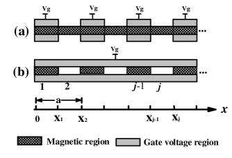
Models and analysis: The geometries we consider are two one-dimensional quantum wires with spatially modulated magnetic potential and spin-orbit coupling illustrated in Fig. 1. In Fig. 1(a), each periodic unit consists of one SOC segment and one non-SOC segment with the same length of ( is set at 20 nm in the following calculations). The magnetic field is applied uniformly along the wire. In Fig. 1(b), the periodic unit consists of one magnetic and one non-magnetic region also with the same length of The gate voltage is laid uniformly along the wire. The symbols of in the figure indicate the applied gate voltages to control the Rashba strengths, which are typically on the order of 10-11 eVm Nitt . To provide a clear illustration, we label the segments in series: , as shown in Fig. 1.
The Hamiltonians of the two modulation structures can be written as a universal formula:
| (1) |
where the effective mass of electrons is set as 0.067 is the mass of the free electron), is the -component of the momentum operator, and is the Pauli spin operator. The denotation is a spin-dependent parameter for the strength of the Zeeman-like potential. The parameter indicates the strength of SOC. Two functions and are introduced to describe the spatial modulations of the magnetic potential and the SOC, respectively. For Fig. 1(a), throughout the wire, and in the odd segments and 0 in the even segments. For Fig. 1(b), throughout the wire, and and 0 in the odd and even segments, respectively.
The wave functions in odd segments and in even segments can be written as:
| (2a) | |||
| (2b) | |||
| The denotations and express the eigenspinor states and Suppose four wave vector functions , and they are expressed as the following: | |||
| (3a) | |||||
| (3b) | |||||
| (3c) | |||||
| (3d) | |||||
| where is the incident electron energy. Then for Fig.1(a), in Eq.(2a), and in Eq.(2b). For Fig.1(b), in Eq.(2a), and in Eq.(2b). Using boundary conditions Mats ; Zuli ; Yao at the interfaces of SOC/non-SOC or magnetic/non-magnetic, we can get the transfer matrix Shi ; Gong1 for the wave functions at and segments and obtain the outgoing spin states. | |||||
Note that the injected current in our scheme is completely unpolarized, which is theoretically simulated by a mixed quantum state of two orthogonal spin states Niko , for example, and are chosen in our calculation. For an incident electron in the spin-up state , the conductance of the outgoing spin-up state is and that of the outgoing spin-down state is Similarly, for an incident electron in the spin-down state , the conductances of the outgoing spin-up and spin-down states are and respectively. The spin polarization along axes is obtained from the formula Niko :
| (4) |
Here we would like to emphasize that any two orthogonal spin states with equal probabilities can be used to simulate the unpolarized current. If we choose orthogonal spin states and to simulate the unpolarized current, the conductance , because and are eigenspinors of the Hamiltonian Eq.(1). Although spin-resolved conductances , , , rely on the the orthogonal component of the injected unpolarized current, the spin polarization does not.
Results and Discussion: Figure 2(a) shows the spin polarization as a function of the Fermi energy for the modulation of Fig. 1 (a), with the Rashba strength is fixed at 0.04 a.u. ( a.u. eVm). When no magnetic potential is applied, the periodic SOC will induce coinciding energy gaps for spin-up and -down electrons Gong1 . No spin polarization is achieved because the gaps for spin-up and -down electrons have the same position and width. The striking feature is that the periodically modulated Rashba potential, even combining with a weak magnetic modulation ( meV), can induce appreciable spin polarization. We get two energy intervals, within which 100% spin polarization with opposite signs are obtained. Increasing the magnetic modulation to meV, the two gaps become farther away from each other. In this scheme, the weak magnetic potential plays the critical role to break the time-reversal symmetry. In addition, we also investigate the case that and meV, no appreciable spin polarization is induced (not shown). This demonstrates that the magnetic potential with the magnitude meV is too small to be an effective spin-selective barrier, yet it is sufficient to break the time reversal symmetry.

To better understand the behavior of the spin polarization in Fig. 2(a), we investigate the spin-resolved conductance. Figure 2(b) shows the spin-up conductance and spin-down conductance as a function of the incident energy. When a weak magnetic potential is applied ( meV), gaps for spin-up and -down are partially separated. Increasing the magnetic modulation to meV, the two gaps are completely separated. For the magnetic modulation, spin-up and -down electrons see different magnetic potentials, while for the Rashba modulation, they see the same Rashba potential. Both the SOC and magnetic potential are indispensable for the spin filter effect: the width of the gaps is determined by the periodic SOC strengths, while the separation of the gaps depends on the application of the magnetic potential.
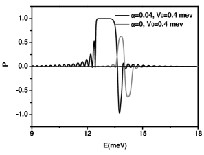
Figure 3(a) displays the spin polarization versus the incident energy for the structure in Fig. 1(b) with the magnetic potential parameter meV. When the Rashba strength , the periodic magnetic modulations can result in 100% spin polarization in two energy intervals Zhou . Here we pay more attention to the influence of the uniform SOC. Applying a nonzero SOC, we find that both the spin-up and -down gaps float toward lower energy region. Comparing the curve corresponding to “ and the one “ it is found that Rashba SOC can inverse the spin polarization from 100% to -100% within certain energy ranges (13.213.8 meV in the Fig. 3(a)). To clearly illustrate this point, we plot Rashba SOC dependence of the spin polarization in Fig. 3(b), in which energy is given as 13.5 meV. A transition from positive to negative polarization is clearly seen, i.e. a positive/negtive spin polarization switching effect is obtained by tuning the SOC strength. The previous schemes for spin filters generally just create polarized current out of an unpolarized source. Here, we provide a more flexible property for spin filter. In addition, we would like to emphasize that in Fig. 1(a) the magnetic field just has the contribution to break the time reversal, while in Fig. 1(b), it must bring an appreciable energy gap. Quantitatively comparing Fig. 2 and Fig. 3(a), we believe that modulation of Fig. 1(a) is more advantageous over that of Fig. 1(b), if the lower magnetic potential is the main factor to be considered.

For the case that both the Rashba SOC and magnetic potential are periodically modulated, some investigations have been conducted previously Wang2 . For the same structure, we obtain different results compared with the report of Ref.Wang2 . No spin polarization can be achieved when the magnetic field is zero in our calculation, because the Rashba spin-orbit coupling can not break the time reversal symmetry Zhai2 . In Ref.Wang2 , however, even when the magnetic field is zero, they obtain the full spin polarization. The critical difference results from that the incident current with spin state in Ref.Wang2 is only unpolarized along axes, but not a completely unpolarized current. For this geometry, it is found that with the application of the periodic SOC, the width of the positive polarization is enlarged, while that of the negative polarization is suppressed, as shown in Fig. 4. For the periodic magnetic modulation, although gaps for spin-up and -down electrons have different positions, yet they have the same width (see Fig. 3(a)), because the width of the gap is determined by the absolute magnitude of the periodic potential. With the presence of the periodic Rashba potential, the balance of the potential strengths for spin-up and -down electrons is upset, which induces the disparity between the positive and negative spin polarization observed in Fig. 4.
Conclusion: Theoretical schemes for spin filter are proposed through investigations on the spin-dependent electron transport in one-dimensional quantum wires with spatially modulated weak magnetic potentials and Rashba spin-orbit couplings. Two kinds of modulation structures are mainly investigated. For case I, by combining the periodic SOC with the weak homogenous magnetic field and two separated gaps for spin-up and -downs electrons are obtained, and therefore full spin polarizations with opposite signs are realized. For case II, the periodic magnetic potential results in two separated gaps, and the spin polarity within the gaps can be switched by the uniform SOC modulation. The spin filters are implemented through experimentally available Rashba interaction and weak magnetic modulation. They may be useful in the future design of spin-based devices.
Acknowledgement: This work was supported by the National Natural Science Foundation of China with grant No 1067027, the Grand Foundation of Shanghai Science and Technology (05DJ14003), and 973-project under grant No. 2006CB921300.
References
- (1) J. C. Egues, C. Gould, G. Richter, and L. W. Molenkamp, Phys. Rev. B 64, 195319 (2001).
- (2) F. Zhai and H. Q. Xu, Appl. Phys. Lett. 88, 032502 (2006).
- (3) M. W. Lu, L. D. Zhang, and X. H. Yan, Phys. Rev. B 66, 224412 (2002).
- (4) X. F. Wang and P. Vasilopoulos. Appl. Phys. Lett. 81, 1636 (2002).
- (5) Y. Guo, B. Gu, Z. Zong, J. Yu, and Y. Kawazone, Phys. Rev. B 62, 2635 (2000).
- (6) J. Zhou, Q. W. Schi, and M. W. Wu, Appl. Phys. Lett. 84, 365 (2004).
- (7) A. E. Popescu and R. Ionicioiu, Phys. Rev. B 69, 245422 (2004).
- (8) M. Khodas, A. Shekhter, and A.M. Finkel’stein, Phys. Rev. Lett. 92, 086602 (2004).
- (9) J. E. Hirsch, Phys. Rev. Lett. 83, 1834 (1999). D. D. Awschalom and M. E. Flatte, Nature Phys. 3, 153 (2007) and references therein.
- (10) Y. A. Bychkov and E. I. Rashba, J. Phys. C 17, 6039 (1984).
- (11) E. N. Bulgakov and A. F. Sadreev, Phys. Rev. B 66, 075331 (2002).
- (12) S. Pramanik, S. Bandyopadhyay, and M. Cahay, IEEE Trans. Nanotechnol. 4, 2 (2005).
- (13) F. Zhai and H. Q. Xu, Phys. Rev. Lett. 94, 246601 (2005).
- (14) P. Strěda and P. Sěba, Physica. E 22, 460 (2004).
- (15) J. Nitta, T. Akazaki, H. Takayanagi, and T. Enoki, Phys. Rev. Lett. 78, 1335 (1997).
- (16) T. Matsuyama, C.-M. Hu, D. Grundler, G. Meier, and U. Merkt. Phys. Rev. B 65, 155322 (2002).
- (17) U. Zülicke and C. Schroll, Phys. Rev. Lett. 88, 029701 (2002).
- (18) J. Yao and Z. Q. Yang, Phys. Rev. B 73, 033314 (2006).
- (19) Y. M. Shi, L. P. Wu, X. F. Cao, X. L. Song, S. P. Zhou, Phys. Lett. A 356, 446 (2006).
- (20) S.J. Gong and Z.Q. Yang, cond-mat/0611362 (unpublished).
- (21) B. K. Nikolić and S. Souma, Phys. Rev. B 71, 195328 (2005).
- (22) L. G. Wang and K. Chang, Solid State commun. 137, 260 (2006).