Enhanced spin-orbit scattering length in narrow AlxGa1-xN/GaN wires
Abstract
The magnetotransport in a set of identical parallel AlxGa1-xN/GaN quantum wire structures was investigated. The width of the wires was ranging between 1110 nm and 340 nm. For all sets of wires clear Shubnikov–de Haas oscillations are observed. We find that the electron concentration and mobility is approximately the same for all wires, confirming that the electron gas in the AlxGa1-xN/GaN heterostructure is not deteriorated by the fabrication procedure of the wire structures. For the wider quantum wires the weak antilocalization effect is clearly observed, indicating the presence of spin-orbit coupling. For narrow quantum wires with an effective electrical width below 250 nm the weak antilocalization effect is suppressed. By comparing the experimental data to a theoretical model for quasi one-dimensional structures we come to the conclusion that the spin-orbit scattering length is enhanced in narrow wires.
I Introduction
The AlxGa1-xN/GaN material system is a very promising candidate for future spin electronic applications. The reason is, that two important requirements for the realization of spin electronic devices are fulfilled in this material class. First, transition-metal-doped GaN diluted magnetic semiconductors have been shown to have high Curie temperatures for injection and detection of spin polarized carriers (see, e.g. Ref. Liu et al., 2005 and references therein) and second, spin-orbit coupling for spin control in non-magnetic AlxGa1-xN/GaN heterostructures was observed.Lo et al. (2002); Tsubaki et al. (2002); Lu et al. (2004); Cho et al. (2005); Weber et al. (2005); Thillosen et al. (2006a); Schmult et al. (2006b); Thillosen et al. (2006b); Schmult et al. (2006a); Kurdak et al. (2006)
Spin-orbit coupling in AlxGa1-xN/GaN two-dimensional electron gases (2DEGs) can be investigated by analyzing the characteristic beating pattern in Shubnikov–de Haas oscillations,Lo et al. (2002); Tsubaki et al. (2002); Lu et al. (2004); Cho et al. (2005) by measuring the circular photogalvanic effect,Weber et al. (2005) or by studying weak-antilocalization.Lu et al. (2004); Thillosen et al. (2006a, b); Schmult et al. (2006a); Kurdak et al. (2006) The latter is an electron interference effect where the random deviations of the spin orientations between time reversed paths result in an enhanced conductance.Hikami et al. (1980); Bergmann (1982); Gusev et al. (1984) From weak antilocalization measurements information on characteristic length scales, i.e. the spin-orbit scattering length and the phase coherence length , can be obtained.
For quasi one-dimensional systems it was predicted theoreticallyBournel et al. (1998); Mal’shukov and Chao (2000); Kiselev and Kim (2000); Pareek and Bruno (2002) and shown experimentallyTh. Schäpers et al. (2006); Wirthmann et al. (2006); Holleitner et al. (2006); Kwon et al. (2007) that can be considerably enhanced compared to the value of the 2DEG. This has important implications for the performance of spin electronic devices, e.g. the spin field-effect-transistor,Datta and Das (1990) since an enhanced value of results in a larger degree of spin polarization in the channel and thus to larger signal modulation.Datta and Das (1990); Bournel et al. (1998) In addition, many of the recently proposed novel spin electronic device structures explicitly make use of one-dimensional channels, because the restriction to only one dimension allows new switching schemes.Nitta et al. (1999); Kiselev and Kim (2001); Governale et al. (2002); Cummings et al. (2006)
Very recently, transport measurements on AlGaN/GaN-based one-dimensional structures, i.e quantum points contacts, have been reported.Chou (2005); Schmult et al. (2006b) With respect to possible spin electronic applications it is of great interest, how the spin transport takes place in AlGaN/GaN quasi one-dimensional structures. Since an enhanced value of is very advantageous for the design of spin electronic devices, it would be very desirable if this effect can be observed in AlxGa1-xN/GaN wire structures.
Here, we report on magnetotransport measurements on AlxGa1-xN/GaN parallel quantum wire structures. We will begin by discussing the basic transport properties of wires with different widths, i.e. resistivity, sheet electron concentration, and mobility. Spin-orbit coupling in our AlxGa1-xN/GaN quantum wires is investigated by analyzing the weak antilocalization effect. We will discuss to which extent the weak antilocalization effect in AlxGa1-xN/GaN heterostructures is affected by the additional confinement in wire structures. By fitting a theoretical model to or experimental data, we will be able to answer the question if the spin-orbit scattering length increases with decreasing wire width, as found in quantum wires fabricated from other types of heterostructures.
II Experimental
The AlGaN/GaN heterostructures were grown by metalorganic vapor phase epitaxy on a (0001) Al2O3 substrate. Two different samples were investigated. Sample 1 consisted of a 3-m-thick GaN layer followed by a 35-nm-thick Al0.20Ga0.80N top layer, while in sample 2 a 40-nm-thick Al0.10Ga0.90N layer was used as a top layer. The quantum wire structures were prepared by first defining a Ti etching mask using electron beam lithography and lift-off. Subsequently, the AlGaN/GaN wires were formed by Ar+ ion beam etching. The etching depth of 95 nm was well below the depth of the AlGaN/GaN interface. The electron beam lithography pattern was chosen so that a number of 160 identical wires, each 620 m long, were connected in parallel. A schematic cross section of the parallel wires is shown in Fig. 1 (inset).
Different sets of wires were prepared comprising a geometrical width ranging from 1110 nm down to 340 nm (see Table 1). The geometrical widths of the wires were determined by means of scanning electron microscopy. The sample geometry with quantum wires connected in parallel was chosen, in order to suppress universal conductance fluctuations.Beenakker and van Houten (1997) After removing the Ti mask by HF, Ti/Al/Ni/Au Ohmic contacts were defined by optical lithography. The Ohmic contacts were alloyed at 900∘C for 30 s. For reference purposes a 100-m-wide Hall bar structure with voltage probes separated by a distance of 410 m were prepared on the same chip.
The measurements were performed in a He-3 cryostat at temperatures ranging from 0.4 K to 4.0 K. The resistances were measured by employing a current-driven lock-in technique with an ac excitation current of 100 nA and 1 A for sample 1 and 2, respectively.
| (nm) | (nm) | () | (cm | (cm2/Vs) | (nm) | (nm) | (nm) | |
|---|---|---|---|---|---|---|---|---|
| 1 | 1090 | 880 | 131 | 5.1 | 9400 | 349 | 550 | 3000 |
| 1 | 880 | 670 | 126 | 5.2 | 9600 | 360 | 600 | 2950 |
| 1 | 690 | 480 | 132 | 4.9 | 9700 | 344 | 700 | 2500 |
| 1 | 440 | 230 | 132 | 5.2 | 9000 | 341 | 1300 | 1550 |
| 1 | 340 | 130 | 136 | 4.5 | 10000 | 343 | 1800 | 1150 |
| 2 | 1110 | 870 | 730 | 2.2 | 4000 | 96 | 500 | 1200 |
| 2 | 930 | 690 | 860 | 2.2 | 3400 | 82 | 520 | 1000 |
| 2 | 720 | 480 | 900 | 2.0 | 3400 | 81 | 640 | 950 |
| 2 | 470 | 230 | 830 | 2.0 | 3800 | 88 | 850 | 900 |
| 2 | 360 | 120 | 740 | 1.9 | 4300 | 100 | 1000 | 670 |
III Results and Discussion
In order to gain information on the transport properties of the AlxGa1-xN/GaN layer systems, Shubnikov–de Haas oscillations were measured on the Hall bar samples. At a temperature of 0.5 K sheet electron concentrations of cm-2 and cm-2, were determined for sample 1 and 2, respectively. The Fermi energies calculated from are 55 meV for sample 1 and 24 meV for sample 2. Here, an effective electron mass of was taken into account.Thillosen et al. (2006b) The mobilities were 9150 cm2/Vs and 3930 cm2/Vs for sample 1 and 2, respectively, resulting in elastic mean free paths of 314 nm and 95 nm. The smaller electron concentration of sample 2 can be attributed to the lower Al-content of the AlxGa1-xN barrier layer resulting in a smaller polarization-doping.Ambacher et al. (2000) The lower mobility found in sample 2 compared to sample 1 can be explained by the reduced screening at lower electron concentrations.Sakowicz et al. (2006)
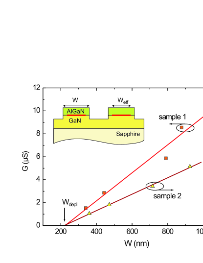
Owing to the large surface potential of GaN, which has been determined to be between 0.5 and 0.6 eV,Kocan et al. (2002) a considerable surface carrier depletion can be expected. For our wires the carrier depletion at the mesa edges will result in an effective electrical width which is smaller than the measured geometrical width . In order to gain information on the lateral width of the depletion zone, the wire conductance at zero magnetic field was determined for different wire widths. In Fig. 1 the single-wire conductance is shown as a function of the wire width for both samples. It can be seen that for both samples scales linearly with . The total width of the depletion zone was determined from the linear extrapolation to , indicated by in Fig. 1.Menschig et al. (1990); Long et al. (1993) The depletion zone width for sample 1 is 210 nm while for sample 2 a value of 240 nm was determined. The larger value of for sample 2 can be attributed to the lower electron concentration compared to sample 1. The corresponding effective electrical width , defined by , is listed in Table 1. The two-dimensional resistivity of the wires at was calculated based on . As can be seen by the values of given in Table 1, for sample 1 the resistivity remains at approximately the same value if the wire width is reduced. A similar behavior is observed for sample 2, although the variations are somewhat larger. In any case no systematic change of is found for both samples.
As can be seen in Fig 2, clear Shubnikov–de Haas oscillations in the magnetoresistivity are resolved for different sets of wires of sample 1. For a better comparison the slowly varying field-dependent background resistivity was subtracted. In order to get an impression on the relation between the amplitude of the Shubnikov–de Haas oscillations and the background resistivity, the total resistivity is shown exemplarily for the 1090-nm-wide wires in Fig. 2 (inset). As can be seen here, the oscillation amplitude turns out to be small compared to , because of the relatively low mobility. From the oscillation period of vs. the sheet electron concentration was determined for the different sets of wires. As can be seen in Fig. 2, the oscillation period and thus is approximately the same for all sets of wires (cf. Table 1). The values of are comparable to the value found for the 2DEG. As given in Table 1, for sample 2 the values of for the different sets of wires were also found to be close to the value extracted from the corresponding Hall bar structure.
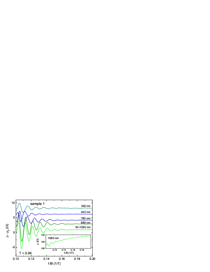
The mobility and elastic mean free path was determined from and . As can be inferred from the values of and given in Table 1, both quantities are similar for all sets of wires for a given heterostructure. For sample 2, is always smaller than , therefore no significant deviation from the 2DEG conductivity is expected. However, for the 440 nm and 340 nm wide wires of sample 1, exceeds so that a boundary scattering contribution is expected. However, since the mobility is not decreased, we can conclude that the boundary scattering is predominately specular. Probably, the smooth potential from the depletion zone favors specular reflection.
We now turn to the investigation of spin-related effects in the electron transport. In Fig. 3(a) the normalized magnetoconductivity is shown for different sets of wires of sample 1. For the narrow wires with a width up to 440 nm the magnetoconductivity monotonously increases for increasing values of , which can be attributed to weak localization. The weak localization effect originates from the constructive interference of time-reversed pathes for the case when spin-orbit scattering can be neglected. In contrast, for the 1090 nm, 880 nm, and 790 nm wide wires, a peak is found in the magnetoconductivity at , which is due to weak antilocalization. The slope of the magnetoconductivity changes sign at mT. This value corresponds well to the positions of the minima found in the weak antilocalization measurements on the Hall bars of sample 1. For magnetic fields beyond 2.2 mT the transport is governed by weak localization, where the magnetoconductivity increases with .
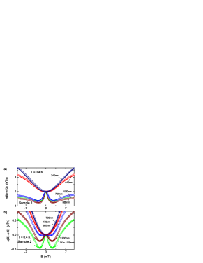
As can be seen in Fig. 3(b), a similar behavior is found for sample 2. For wire widths up to 470 nm weak localization is observed, whereas for the 1110 nm, 930 nm and 720 nm wide wires weak antilocalization is found. In contrast to sample 1, the width of the weak antilocalization peak depends on the widths of the wires. For the first two sets of wires minima in are found at mT. Whereas, for the 720-nm-wide wires minima are observed at mT. The peak height due to weak antilocalization decreases with decreasing wire width. In general, the modulations of are found to be considerably smaller for sample 2 compared to sample 1, which can be attributed to the smaller elastic mean free path and, as it will be shown later, to the smaller phase coherence length.
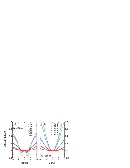
With increasing temperature the weak antilocalization peak decreases. This can be seen in Fig. 4(a), where is shown at different temperatures for the 930-nm-wide wires of sample 2. Above 2 K no signature of weak antilocalization is found anymore. Furthermore, the weak localization contribution to successively decreases with increasing temperature. This effect can be attributed to the decreasing phase coherence length with increasing temperature.Al’tshuler et al. (1982); Choi et al. (1987) As can be seen in Fig. 4(b), for the 360-nm-wide wires only weak localization was observed. Similar to the wider sets of wires, the weak localization effect is damped with increasing temperatures.
From weak antilocalization measurements the characteristic length scales, i.e. and , can be estimated. In order to get some reference value for the 2DEG, the model developed by Iordanskii, Lyanda-Geller, and PikusIordanskii et al. (1994) (ILP-model) was fitted to the weak antilocalization measurements of the Hall bar structures. Only the Rashba contribution was considered, here. For sample 1, and were found to be 1980 nm and 300 nm at 0.5 K, respectively, whereas for sample 2 the corresponding values were 1220 nm and 295 nm at 0.4 K. For both samples the effective spin-orbit coupling parameter is approximately eVm. The zero-field spin-splitting energy can be estimated by using the the expression , with the Fermi wavenumber given by . For sample 1 one obtains a value of meV, while for sample 2 one finds 0.43 meV. The values of are relatively large compared to their corresponding Fermi energies, which confirms the presence of a pronounced spin-orbit coupling in AlxGa1-xN/GaN 2DEGs.Thillosen et al. (2006a, b); Schmult et al. (2006a); Kurdak et al. (2006)
The ILP-model is only valid for 2DEGs with , thus it cannot be applied to our wire structures. Very recently, a model appropriate for wire structures was developed by Kettemann,Kettemann (2006) which covers the case . Here, the quantum correction to the conductivity is given by:
| (1) | |||||
with defined by and given by . The effective external magnetic field is defined by:
| (2) |
with the magnetic length. The spin-orbit scattering length in the wire can be obtained from the characteristic spin-orbit field .
The Kettemann model was fitted to the experimental curves by adjusting and . The corresponding values of and extracted from the fit are listed in Table 1 and shown in Fig. 5. Even for the widest wires is found to be larger than the value obtained for the 2DEG from the ILP fit. The deviations are probably already due to confinement effects. In addition, different approximations made in ILP modelIordanskii et al. (1994) for the two-dimensional case and the Kettemann modelKettemann (2006) for wire structures might also account partially for the deviations.
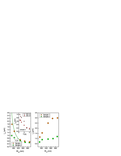
As can been seen in Fig 5, for sample 1 the spin-orbit scattering length monotonously increases with decreasing , while decreases. The latter is in accordance to theoretical predictions.Al’tshuler et al. (1982); Choi et al. (1987) For the wider wires with nm, 880 nm, and 790 nm exceeds , so that weak antilocalization is expected. In contrast, for the very narrow wires with nm and 130 nm the values for obtained from the fit are close or even exceed . In this case the spin-rotation caused by spin-orbit coupling is not sufficiently strong to affect the interference of time-reversed paths.Knap et al. (1996) As a consequence, the weak antilocalization effect is suppressed so that weak localization remains. For the 340-nm-wide wires a satisfactory fit could be obtained down to a lower boundary value of , indicated by the half filled symbol shown in Fig. 5(a). In principle, one could argue, that the appearance of weak localization for the very narrow wires is solely due to a strongly reduced phase coherence length, while remains at the relatively low values found for the wider wires. However, in our fits the suppression of the weak antilocalization effect could not be explained by simply decreasing compared to the values of the wider wires. A satisfactory fit was only obtained if was increased to a larger value compared to the wider wires.
As can be seen in Fig 5, for sample 2 the spin-orbit scattering length also increases with decreasing , although with a smaller slope, compared to sample 1. Similarly to sample 1, decreases with decreasing wire width. However, due to the lower elastic mean free path of sample 2, is considerably smaller for this sample (cf. Fig. 5). All values of and obtained from the fit are listed in Table 1. A comparison of for the widest wires and for the Hall bar structures reveals, that the weak antilocalization peak is larger by a factor of two. Thus, although is significantly smaller than this clearly indicates that the additional carrier confinement already affects the interference effects.Beenakker and van Houten (1997)
By fitting the Kettemann model to the measurements shown in Fig. 4, was determined for the 930 nm and 360 nm wide wire at different temperatures. For both samples a fixed value of , corresponding to the values at 0.4 K, were assumed. As can be seen in Fig. 5(a), inset, for both samples monotonously decreases with temperature, in accordance with theoretical models.Al’tshuler et al. (1982); Choi et al. (1987) At a temperature of 4 K is found to be close to . In that regime the interference effects are expected to be suppressed. This is confirmed by the measurements where only a weak field-dependence of is found.
For both samples we found an increase of with decreasing wire width and even a suppression of weak antilocalization for narrow wires. This observance is in accordance with weak antilocalization measurements of quantum wires based on low-band gap materials, i.e. InGaAs or InAs.Th. Schäpers et al. (2006); Wirthmann et al. (2006) However, for these types of quantum wells the coupling parameter is usually very large. In this case transport takes place in a different regime where so that a more elaborate model had to be applied to extract .Th. Schäpers et al. (2006) As discussed by Kettemann,Kettemann (2006) the increase of can be attributed solely to a modification of the backscattering amplitude. In an intuitive picture, the increase of in narrow wires can be explained, by the reduced magnitude of accumulated random spin phases due to the elongated shape of relevant closed loops. Here, the spin phase accumulated in forward direction is basically compensated by the propagation in backwards direction, so that the spin-related contribution to the interference of electrons backscattered on time reversed paths tends to diminish. As a result, only weak localization is observed.Bournel et al. (1998); Th. Schäpers et al. (2006) Although the spin-orbit coupling strength in our AlGaN/GaN samples is small compared to heterostructures based on InAs and thus different models have to be consulted for a detailed description, the basic mechanism responsible for a suppression of the weak antilocalization effect is the same for both material systems. In our case, no decrease of spin-orbit coupling strength, quantified by , is required to account for the suppression of weak antilocalization in narrow wires. In fact, an estimation of effect of the confinement potential on based on the theory of Moroz and BarnesMoroz and Barnes (1987) confirmed that for our wire structures no significant change of with is expected. As shown in Fig. 5 (a), for sample 2 the increase of with decreasing wire width is smaller than for sample 1. We attribute this to the fact, that for sample 2 the larger extend of diffusive motion, quantified by the smaller value of , partially mask the effect of carrier confinement. Due to the larger values of and of sample 1 compared to sample 2, the shape of the loops responsible for interference effect is affected more by the confinement of the wire. Thus, the enhancement of is expected to be stronger. Indeed, theoretical calculations by Pareek and BrunoPareek and Bruno (2002) showed that for quasi-onedimensional channels a strong increase of can only be expected if is in the order of .
For narrow wires with in the diffusive regime () the spin-orbit scattering lengths can be estimated by:Kettemann (2006)
| (3) |
Here, is the spin-orbit scattering length of the 2DEG. The calculated values of should only be compared to the fitted values of of sample 2, since only for this sample is fulfilled. As can be seen in Fig. 5 (a), calculated from Eq. (3) fits well to the experimental values corresponding to intermediate effective wire width of nm. However, for smaller effective wire widths the calculated values of are considerably larger. Probably, spin scattering processes other than the pure Rashba contribution are responsible for this discrepancy.Kettemann (2006)
An enhanced spin-orbit scattering length is very desirable for spin electronic devices. Providing that the strength of the spin-orbit coupling itself remains unchanged, a confinement to a quasi one-dimensional system would result in a reduced spin randomization. A reduction of spin randomization is an advantage for the realization of spin electronic devices, since it would ease the constraints regarding the size of these type of devices. In this respect, our finding that increases with decreasing wire width is an important step towards the realization of spin electronic devices based on AlGaN/GaN heterostructures.
IV Conclusions
In conclusion, the magnetotransport of AlGaN/GaN quantum wires had been investigated. Even for sets of quantum wires with a geometrical width as low as 340 nm, clear Shubnikov–de Haas oscillations were observed. Magnetotransport measurements close to zero magnetic field revealed a suppression of the weak antilocalization effect for very narrow quantum wires. By comparing the experimental data with a theoretical model for one-dimensional structures it was found that the spin-orbit scattering length is enhanced in narrow wires. The observed phenomena might have a important implication regarding the realization of spin electronic devices based on AlGaN/GaN heterostructures.
The authors are very thankful to S. Kettemann, Hamburg University, for fruitful discussions and H. Kertz for assistance during low temperature measurements.
References
- Liu et al. (2005) C. Liu, F. Yun, and H. Morkoc, J. Mat. Sci.: Materials in Electronics 16, 555 (2005).
- Lo et al. (2002) I. Lo, J. K. Tsai, W. J. Yao, P. C. Ho, L. W. Tu, T. C. Chang, S. Elhamri, W. Mitchel, K. Y. Hsieh, J. H. Huang, et al., Phys. Rev. B 65, 161306(R) (2002).
- Tsubaki et al. (2002) K. Tsubaki, N. Maeda, T. Saitoh, and N. Kobayashi, Appl. Phys. Lett. 80, 3126 (2002).
- Lu et al. (2004) J. Lu, B. Shen, N. Tang, D. J. Chen, H. Zhao, D. W. Liu, R. Zhang, Y. Shi, Y. D. Zheng, Z. J. Qiu, et al., Appl. Phys. Lett. 85 (2004).
- Cho et al. (2005) K. Cho, T.-Y. Huang, H.-S. Wang, M.-G. Lin, T.-M. Chen, C.-T. Liang, and Y. F. Chen, Appl. Phys. Lett. 86, 222102 (2005).
- Weber et al. (2005) W. Weber, S. Ganichev, Z. Kvon, V. Bel’kov, L. Golub, S. Danilov, D. Weiss, W. Prettl, H.-I. Cho, and J.-H. Lee, Appl. Phys. Lett. 87, 262106 (2005).
- Thillosen et al. (2006a) N. Thillosen, Th. Schäpers, N. Kaluza, H. Hardtdegen, and V. A. Guzenko, Appl. Phys. Lett. 88, 022111 (2006a).
- Schmult et al. (2006b) S. Schmult, M. J. Manfra, A. M. Sergent, A.Punnoose, H. T. Chou, D. Goldhaber-Gordon, and R. J. Molnar, Phys. Stat. Sol. B 243, 033302 (2006b).
- Thillosen et al. (2006b) N. Thillosen, S. Cabanas, N. Kaluza, V. A. Guzenko, H. Hardtdegen, and Th. Schäpers, Phys. Rev. B 73, 241311(R) (2006b).
- Schmult et al. (2006a) S. Schmult, M. J. Manfra, A. Punnoose, A. M. Sergent, K. W. Baldwin, and R. J. Molnar, Phys. Rev. B 74, 033302 (2006a).
- Kurdak et al. (2006) C. Kurdak, N. Biyikli, U. Ozgur, H. Morkoc, and V. I. Litvinov, Phys. Rev. B 74, 113308 (2006).
- Hikami et al. (1980) S. Hikami, A. I. Larkin, and Y. Nagaoka, Progr. Theor. Phys. 63, 707 (1980).
- Bergmann (1982) G. Bergmann, Sol. State Comm. 42, 815 (1982).
- Gusev et al. (1984) G. M. Gusev, Z. D. Kvon, and V. N. Ovsyuk, J. Phys. C: Solid Stad Phys. 17, L683 (1984).
- Bournel et al. (1998) A. Bournel, P. Dollfus, P. Bruno, and P. Hesto, Eur. Phys. J. Appl. Phys. 4, 1 (1998).
- Mal’shukov and Chao (2000) A. G. Mal’shukov and K. A. Chao, Phys. Rev. B 61, R2413 (2000).
- Kiselev and Kim (2000) A. A. Kiselev and K. W. Kim, Phys. Rev. B 61, 13115 (2000).
- Pareek and Bruno (2002) T. P. Pareek and P. Bruno, Phys. Rev. B 65, 241305(R) (2002).
- Th. Schäpers et al. (2006) Th. Schäpers, V. A. Guzenko, M. G. Pala, U. Zülicke, M. Governale, J. Knobbe, and H. Hardtdegen, Phys. Rev. B 74, 081301(R) (2006).
- Wirthmann et al. (2006) A. Wirthmann, Y. S. Gui, C. Zehnder, D. Heitmann, C.-M. Hu, and S. Kettemann, Physica E 34, 493 (2006).
- Holleitner et al. (2006) A. W. Holleitner, V. Sih, R. C. Myers, A. C. Gossard, and D. D. Awschalom, Phys. Rev. Lett. 97, 036805 (2006).
- Kwon et al. (2007) J. H. Kwon, H. C. Koo, J. Chang, and S.-H. Han, Appl. Phys. Lett. 90, 0112505 (2007).
- Datta and Das (1990) S. Datta and B. Das, Appl. Phys. Lett. 56, 665 (1990).
- Nitta et al. (1999) J. Nitta, F. E. Meijer, and H. Takayanagi, Appl. Phys. Lett. 75, 695 (1999).
- Kiselev and Kim (2001) A. A. Kiselev and K. W. Kim, Appl. Phys. Lett. 78, 775 (2001).
- Governale et al. (2002) M. Governale, D. Boese, U. Zülicke, and C. Schroll, Phys. Rev. B 65, 140403(R) (2002).
- Cummings et al. (2006) A. W. Cummings, R. Akis, and D. K. Ferry, Appl. Phys. Lett. 89, 172115 (2006).
- Chou (2005) H. T. Chou, S. Lüscher, D. Goldhaber-Gordon, M. J. Manfra, A. M. Sergent, K. W. West, and R. J. Molnar, Appl. Phys. Lett. 86, 073108 (2005).
- Beenakker and van Houten (1997) C. W. J. Beenakker and H. van Houten, Rev. Mod. Phys. 69, 731 (1997).
- Kettemann (2006) S. Kettemann, Phys. Rev. Lett. 98, 176808 (2007).
- Ambacher et al. (2000) O. Ambacher, B. Foutz, J. Smart, J. R. Shealy, N. G. Weimann, K. Chu, M. Murphy, A. J. Sierakowski, W. J. Schaff, and L. F. Eastman, J. Appl. Phys. 87, 334 (2000).
- Sakowicz et al. (2006) M. Sakowicz, R. Tauk, J. Lusakowski, A. Tiberj, W. Knap, Z. Bougrioua, M. Azize, P. Lorenzini, K. Karpierz, and M. Grynberg, J. Appl. Phys. 100, 113726 (2006).
- Kocan et al. (2002) M. Kocan, A. Rizzi, H. Lüth, S. Keller, and U. K. Mishra, Phys. Stat. Sol. B 234, 773 (2002).
- Menschig et al. (1990) A. Menschig, A. Forchel, B. Ross, R. Germann, W. Heuring, and D. Grützmacher, Micro. Electron. Eng. 11, 11 (1990).
- Long et al. (1993) A. R. Long, M. Rahman, I. K. MacDonald, M. Kinsler, S. P. Beaumont, C. D. W. Wilkinson, and C. R. Stanley, Semicond. Sci. Technol. 8, 39 (1993).
- Al’tshuler et al. (1982) B. L. Al’tshuler, A. G. Aronov, and D. E. Khmelnitsky, J. Phys. C (Sol. State Phys.) 15, 7367 (1982).
- Choi et al. (1987) K. K. Choi, D. C. Tsui, and K. Alavi, Phys. Rev. B 36, 7751 (1987).
- Iordanskii et al. (1994) S. V. Iordanskii, Y. B. Lyanda-Geller, and G. E. Pikus, JETP Lett. 60, 206 (1994).
- Knap et al. (1996) W. Knap, C. Skierbiszewski, A. Zduniak, E. Litwin-Staszewska, D. Bertho, F. Kobbi, J. L. Robert, G. E. Pikus, F. G. Pikus, S. V. Iordanskii, V. Mosser, K. Zekentes, and Yu. B. Lyanda-Geller, et al., Phys. Rev. B 53, 3912 (1996).
- Moroz and Barnes (1987) A. V. Moroz, and C. H. W. Barnes, Phys. Rev. B 61, R2464 (2000).