Theory of tunneling conductance of graphene NIS junctions
Abstract
We calculate the tunneling conductance of a graphene normal metal-insulator-superconductor (NIS) junction with a barrier of thickness and with an arbitrary voltage applied across the barrier region. We demonstrate that the tunneling conductance of such a NIS junction is an oscillatory function of both and . We also show that the periodicity and amplitude of such oscillations deviate from their universal values in the thin barrier limit as obtained in earlier work [Phys. Rev. Lett. 97, 217001 (2006)] and become a function of the applied voltage . Our results reproduces the earlier results on tunneling conductance of such junctions in the thin [Phys. Rev. Lett. 97, 217001 (2006)] and zero [Phys. Rev. Lett. 97, 067007 (2006)] barrier limits as special limiting cases. We discuss experimental relevance of our results.
pacs:
74.45+c, 74.78.NaI Introduction
Graphene, a two-dimensional single layer of graphite, has been recently fabricated by Novoselov et. al. nov1 . This has provided an unique opportunity for experimental observation of electronic properties of graphene which has attracted theoretical attention for several decades oldref . In graphene, the energy bands touch the Fermi energy at six discrete points at the edges of the hexagonal Brillouin zone. Out of these six Fermi points, only two are inequivalent; they are commonly referred to as and points ando1 . The quasiparticle excitations about these and points obey linear Dirac-like energy dispersion. The presence of such Dirac-like quasiparticles is expected to lead to a number of unusual electronic properties in graphene including relativistic quantum Hall effect with unusual structure of Hall plateaus shar1 . Recently, experimental observation of the unusual plateau structure of the Hall conductivity has confirmed this theoretical prediction nov2 . Further, as suggested in Ref. geim1, , the presence of such quasiparticles in graphene provides us with an experimental test bed for Klein paradox. klein1
Another, less obvious but nevertheless interesting, consequence of the existence Dirac-like quasiparticles can be understood by studying tunneling conductance of a normal metal-superconductor (NS) interface of graphene beenakker1 . Graphene is not a natural superconductor. However, superconductivity can be induced in a graphene layer in the presence of a superconducting electrode near it via proximity effect volkov1 ; beenakker1 ; beenakker2 or by possible intercalation with dopant molecules uchoa1 . It has been recently predicted beenakker1 that a graphene NS junction, due to the Dirac-like energy spectrum of its quasiparticles, can exhibit specular Andreev reflection in contrast to the usual retro reflection observed in conventional NS junctions andreev1 ; tinkham1 . Such specular Andreev reflection process leads to qualitatively different tunneling conductance curves compared to conventional NS junctions beenakker1 . The effect of the presence of a thin barrier region of thickness created by applying a large gate voltage ( such that is finite) between the normal and the superconducting region has also been studied in Ref. bhattacharya1, . It has been shown that in this thin barrier limit, in contrast to all normal metal-insulator-superconductor (NIS) junctions studied so far, the tunneling conductance of a graphene NIS junction is an oscillatory function of the dimensionless barrier strength , where denotes the Fermi velocity of graphene, with periodicity . Further, it has also been demonstrated that the tunneling conductance reaches its maxima of for , where is an integer. The latter result was also interpreted in terms of transmission resonance property of the Dirac-Bogoliubov quasiparticles nov2 . However, no such studies have been undertaken for NIS junctions with barriers of arbitrary thickness and barrier potential .
In this work, we extend the analysis of Ref. bhattacharya1, and calculate the tunneling conductance of a graphene NIS junction with a barrier of thickness and with an arbitrary voltage applied across the barrier region. The main results of our work are the following. First, we show that the oscillatory behavior of the tunneling conductance is not a property of the thin barrier limit, but persists for arbitrary barrier width and applied gate voltage , as long as , where is the coherence length of the superconductor. Second, we demonstrate that the periodicity and amplitude of these oscillations deviate from their values in the thin barrier limit and becomes a function of the applied voltage . We point out that the barriers which can be realistically achieved in current experimental setups nov2 do not necessarily fall in the thin barrier regime which necessitates a detailed study of arbitrary barriers as undertaken here. Finally, we show that our analysis correctly reproduces the tunneling conductance for both zero barrier beenakker1 and thin barrier bhattacharya1 as limiting cases.
The organization of the rest of the paper is as follows. In Sec. II, we develop the theory of tunneling conductance for a barrier of thickness and with a voltage applied across the barrier region and demonstrate that they correctly reproduce the results of Refs. bhattacharya1, and beenakker1, as limiting cases. The results obtained from this theory is discussed in Sec. III. Finally, in Sec. IV, we discuss possible experiments that can be performed to test our theory.
II Calculation of tunneling conductance
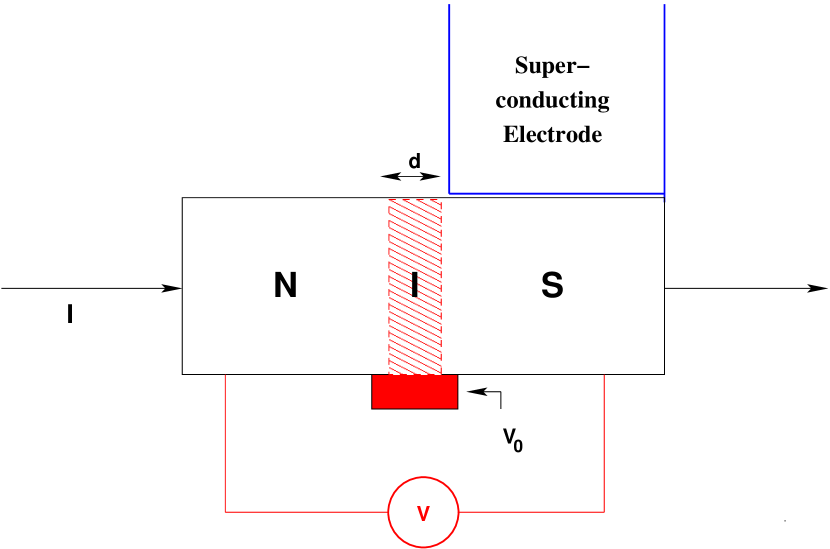
Let us consider a NIS junction in a graphene sheet occupying the plane with the normal region occupying for all as shown schematically in Fig. 1. The region I, modeled by a barrier potential , extends from to while the superconducting region occupies . Such a local barrier can be implemented by either using the electric field effect or local chemical doping geim1 ; nov2 . The region is to be kept close to an superconducting electrode so that superconductivity is induced in this region via proximity effect volkov1 ; beenakker1 . In the rest of this work, we shall assume that the barrier region has sharp edges on both sides. This condition requires that , where and are Fermi wave-vector and wavelength for graphene, and can be realistically created in experiments geim1 . The NIS junction can then be described by the Dirac-Bogoliubov-de Gennes (DBdG) equations beenakker1
| (3) | |||
| (4) |
Here, are the component wavefunctions for the electron and hole spinors, the index denote or for electron/holes near and points, takes values for , denote the Fermi energy which can be made non-zero either by doping or by applying a potential to the graphene sheet, and denote the two inequivalent sites in the hexagonal lattice of graphene, and the Hamiltonian is given by
| (5) |
In Eq. 5, denotes the Fermi velocity of the quasiparticles in graphene and takes values for . The pair-potential in Eq. 4 connects the electron and the hole spinors of opposite Dirac points. We have modeled the pair-potential as
| (6) |
where and are the amplitude and the phase of the induced superconducting order parameter respectively and denotes the Heaviside step function.
The potential gives the relative shift of Fermi energies in normal, insulating and superconducting regions of graphene and can be modeled as
| (7) |
The gate potential can be used to tune the Fermi surface mismatch between the normal and the superconducting regions. Notice that the mean-field conditions for superconductivity are satisfied as long as ; thus, in principle, for large one can have regimes where beenakker1 .
Eq. 4 can be solved in a straightforward manner to yield the wavefunction in the normal, insulating and the superconducting regions. In the normal region, for electron and holes traveling the direction with a transverse momentum and energy , the (unrenormalized) wavefunctions are given by
| (8) |
where the wave-vector for the electron (hole) wavefunctions are given by
| (9) |
and is the angle of incidence of the electron (hole).
In the barrier region, one can similarly obtain
| (10) |
for electron and holes moving along . Here the angle of incidence of the electron(hole) and the wavevector are given by is
| (11) |
Note that Eq. 10 ceases to be the solution of the Dirac equation (Eq. 4) when and . For these parameter values, Eq. 4 in the barrier region becomes which do not have purely oscillatory solutions. For the rest of this work, we shall restrict ourselves to the regime .
In the superconducting region, the BdG quasiparticles are mixtures of electron and holes. Consequently, the wavefunctions of the BdG quasiparticles moving along with transverse momenta and energy , for , has the form
| (12) |
where is the angle of incidence for the quasiparticles. Here the wavevector and the localization length can be expressed as a function of the energy and the transverse momenta as
| (13) |
where is given by
| (14) | |||||
Note that for , becomes imaginary and the quasiparticles can propagate in the bulk of the superconductor.
Next we note that for the Andreev process to take place, the angles , and must all be less than . This sets the limit of maximum angle of incidence . Using Eqns. 8 and 11, one finds that the critical angle of incidence is
| (15) |
Note that in the thin or zero barrier limits treated in Refs. bhattacharya1, and beenakker1, , for all parameter regimes.
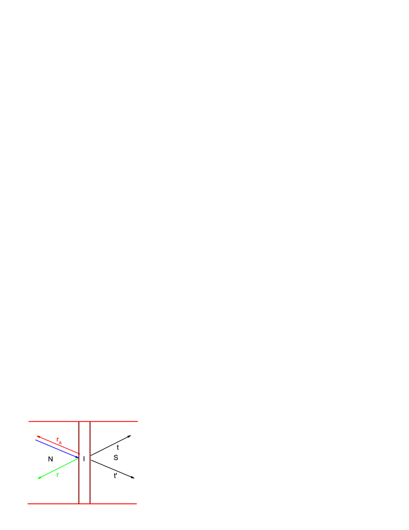
Let us now consider a electron-like quasiparticle incident on the barrier from the normal side with an energy and transverse momentum . The basic process of ordinary and Andreev reflection that can take place at the interface is schematically sketched in Fig. 2. As noted in Ref. beenakker1, , in contrast to conventional NIS junction, graphene junctions allow for both retro and specular Andreev reflections. The former dominates when so that (Eq. 8) while that latter prevails when with . Note that in Fig. 2, we have chosen to denote a retro Andreev reflection for illustration purposes. In practice, includes both retro and specular Andreev reflections. In what follows, we shall denote the total probability amplitude of Andreev reflection as which takes into account possibilities of both retro and specular Andreev reflections.
The wave functions in the normal, insulating and superconducting regions, taking into account both Andreev and normal reflection processes, can then be written as tinkham1
| (16) |
where and are the amplitudes of normal and Andreev reflections respectively, and are the amplitudes of electron-like and hole-like quasiparticles in the superconducting region and , , and are the amplitudes of electron and holes in the barrier. These wavefunctions must satisfy the appropriate boundary conditions:
| (17) |
Notice that these boundary conditions, in contrast their counterparts in standard NIS interfaces, do not impose any constraint on derivative of the wavefunctions at the boundary. These boundary conditions yield
| (18) |
Using the boundary conditions (Eq. 18), one can now solve for the coefficients , , and in Eq. 16. After some straightforward but cumbersome algebra, we find that
| (19) | |||||
| (20) | |||||
| (21) | |||||
| (22) | |||||
| (23) | |||||
| (24) |
where the parameters and can be expressed in terms of , , , , , and (Eqs. 8, 11, 12, and 14) as
| (25) | |||||
| (26) | |||||
| (27) |
The tunneling conductance of the NIS junction can now be expressed in terms of and by tinkham1
where is the ballistic conductance of metallic graphene, denotes the bias voltage, and denotes the number of available channels for a graphene sample of width . For , is a constant. Eq. LABEL:tc1 can be evaluated numerically to yield the tunneling conductance of the NIS junction for arbitrary parameter values. We note at the outset, that when . This occurs in two situations. First, when and so that vanishes. For this situation to arise, which means that has to be finite. Second, when and , so that the zero-bias conductance vanishes when the barrier potential matches the Fermi energy of the normal side comment1 .
We now make contact with the results of Ref. bhattacharya1, in the thin barrier limit. We note that since there are no condition on the derivatives of wavefunctions in graphene NIS junctions, the standard delta function potential approximation for thin barrier tinkham1 can not be taken the outset, but has to be taken at the end of the calculation. This limit is defined as and such that the dimensionless barrier strength
| (29) |
remains finite. In this limit, as can be seen from Eqs. 8, 11 and 12, and so that the expressions for , and (Eq. 27)
| (30) |
where the superscript ”” denotes thin barrier. Using the above-mentioned relations, we also obtain
| (31) |
Eqs. 30 and 31 are precisely the result obtained in Ref. bhattacharya1, for the tunneling conductance of a thin graphene NIS junction. The result obtained in Ref. beenakker1, can be now easily obtained from Eqs. 30 and 31 by substituting in these equations, as also noted in Ref. bhattacharya1, .
III Results
III.1 Qualitative Discussions
In this section, we shall analyze the formulae for tunneling conductance obtained in Sec. II. First we aim to obtain a qualitative understanding of the behavior of the tunneling conductance for finite barrier strength. To this end, we note from Eq. LABEL:tc1 that the maxima of the tunneling conductance must occur where is minimum. In fact, if for all transverse momenta, the tunneling conductance reaches its value . Therefore we shall first try to analyze the expression of (Eq. 19) for subgap voltages and when the Fermi surfaces of the normal and superconducting sides are aligned with each other (). In this case, we need . So for subgap tunneling conductance, we have . In this limit, (Eqs. 8 and 12), , and (Eq. 11). Using these, one can write
| (32) | |||||
| (33) |
Substituting Eq. 33 in the expression of , we find that the numerator of the reflection amplitude becomes (Eqs. 19 and 20)
| (34) | |||||
From the expression of (Eq. 34), we note the following features. First, for normal incidence () where , and hence (Eq. 19) vanishes. Thus the barrier is reflectionless for quasiparticles which incident normally on the barrier for arbitrary barrier thickness and strength of the applied voltage . This is a manifestation of Klein paradox for Dirac-Bogoliubov quasiparticles klein1 . However, this feature is not manifested in tunneling conductance ( Eq. LABEL:tc1) which receives contribution from all angles of incidence. Second, apart from the above-mentioned cases, never vanishes for all angles of incidence and arbitrary unless . Thus the subgap tunneling conductance is not expected to reach a maximum value of as long as the thin barrier limit is not satisfied. However, in practice, for barriers with , the difference between and turns out to be small for all ( for and ) so that the contribution to (Eq. 34) from the terms becomes negligible. Thus can become quite small for special values of for all so that the maximum value of tunneling conductance can reach close to . Third, for large , for which the contribution of terms becomes negligible, and hence becomes very small when the applied voltage matches the gap edge (Eq. 34). Thus the tunneling conductance curves approaches close to its maximum value and becomes independent of the gate voltage at the gap edge for , as is also seen for conventional NIS junctions tinkham1 . Fourth, in the thin barrier limit, ( and ), and , so that the contribution of the terms in Eq. 34 vanishes and one gets
| (36) | |||||
| (37) | |||||
As noted in Ref. bhattacharya1, , and hence (Eq. 31) vanishes at which yields the transmission resonance condition for NIS junctions in graphene. Fifth, as can seen from Eqs. 19 and 24, both and are periodic functions of and since both and depend on . Thus the oscillatory behavior of subgap tunneling conductance as a function of applied gate voltage or barrier thickness is a general feature of graphene NIS junctions with . However, unlike the thin barrier limit, for an arbitrary NIS junction, , and . Thus the period of oscillations of and will depend on and should deviate from their universal value in the thin barrier limits. Finally, we note from Eqs. 19, LABEL:tc1 and 36 that in the thin barrier limit (and therefore for large ), the amplitude of oscillations of the zero-bias conductance for a fixed , defined as , which depends on the difference of and becomes independent of or the applied gate voltage .
III.2 Numerical Results
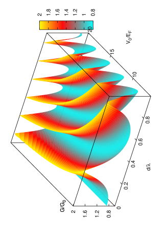
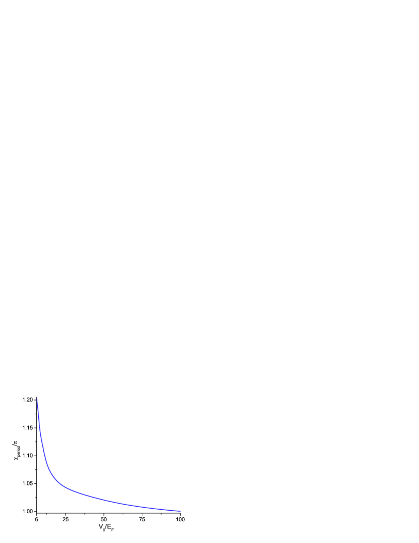
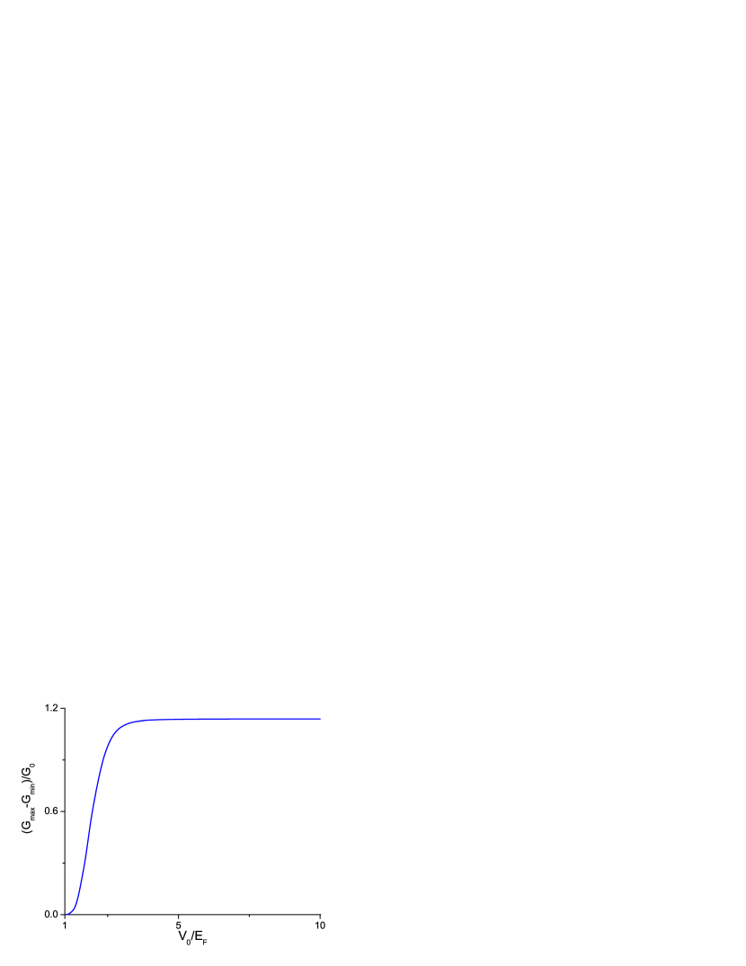
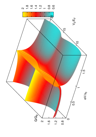
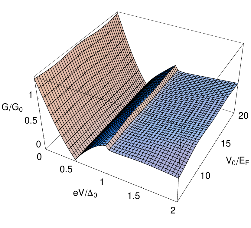
The above-mentioned discussion is corroborated by numerical evaluation of the tunneling conductance as shown in Figs. 3, 4, 5 and 6. From Fig. 3, which plots zero-bias tunneling conductance as a function of and , we find that is an oscillatory function of both and and reaches close to its maximum value of throughout the plotted range of and . Further, as seen from Fig. 4, the periodicity of these oscillations becomes a function of . To measure the periodicity of these oscillations, the tunneling conductance is plotted for a fixed as a function of . The periodicity of the conductance is noted down from these plots and is computed. Fig. 4 clearly shows that deviate significantly from their thin barrier value for low enough and diverges at comment2 . Fig. 5 shows the amplitude of oscillations of zero-bias conductance as a function of . We note that maximum of the zero-bias tunneling conductance reaches close to for . For , the amplitude becomes independent of the applied voltage as in the thin barrier limit, as shown in Fig. 5. For , , so that and hence the amplitude vanishes. Finally, in Fig. 6, we plot the tunneling conductance as a function of the applied bias-voltage and applied gate voltage for . We find that, as expected from Eq. 36, reaches close to at the gap edge for all . Also, as in the thin barrier limit, the oscillation amplitudes for the subgap tunneling conductance is maximum at zero-bias and shrinks to zero at the gap edge , where the tunneling conductance become independent of the gate voltage.
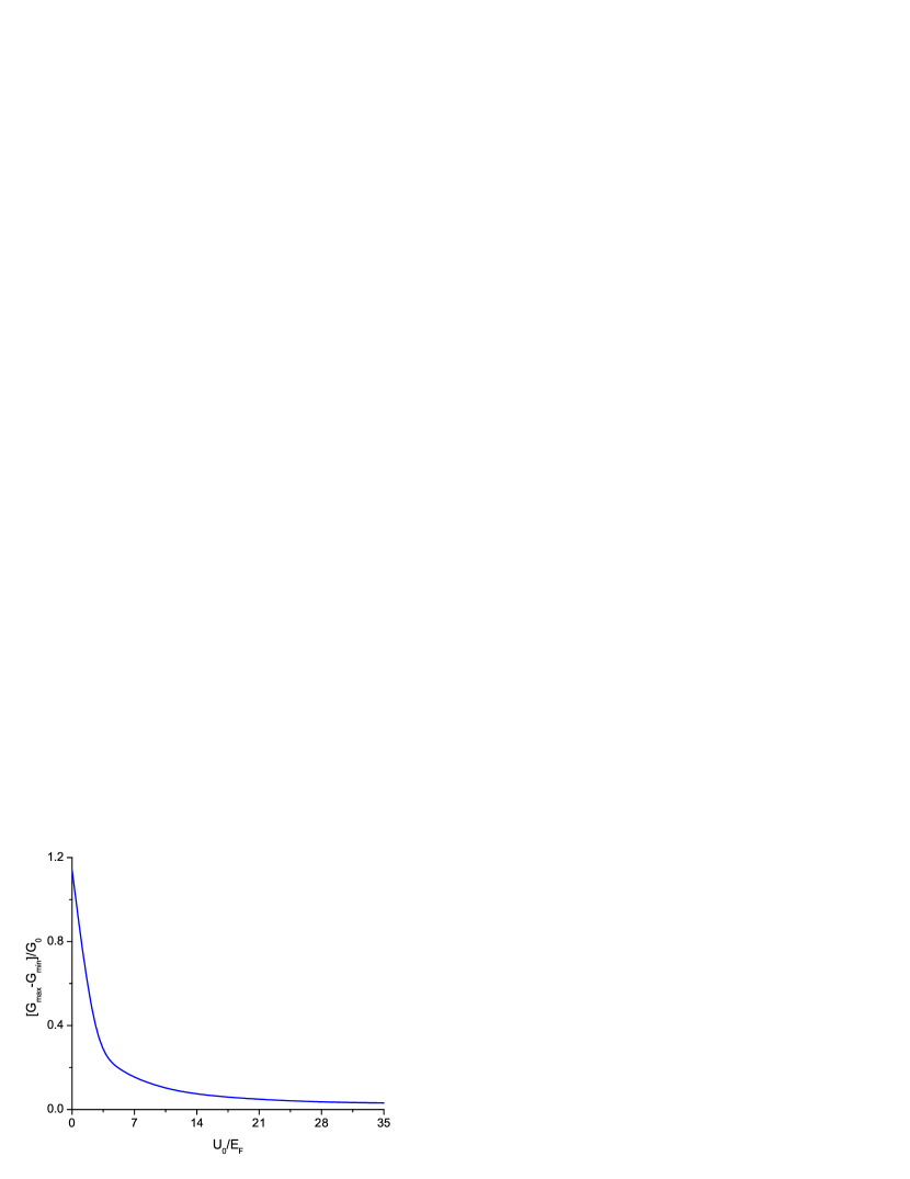
Next, we consider the case , so that . In this regime, there is a large mismatch of Fermi surfaces on the normal and superconducting sides. Such a mismatch is well-known to act as an effective barrier for NIS junctions. Consequently, additional barrier created by the gate voltage becomes irrelevant, and we expect the tunneling conductance to become independent of the applied gate voltage . Also note that at , (Eq. 15). Hence there is no Andreev reflection and consequently vanishes for all values of the applied gate voltage for this bias voltage. Our results in this limit, coincides with those of Ref. beenakker1, . Finally in Fig. 8, we show the dependence of amplitude of oscillation of zero-bias tunneling conductance on for the applied bias voltages and . As expected, the oscillation amplitude with decreases monotonically with increasing . We have verified that this feature is independent of the applied gate voltage as long as .
IV Experiments
Superconductivity has recently been experimentally realized in graphene delft1 . In our proposed experiment, one needs to realize an NIS junction in graphene. The local barrier can be fabricated using methods of Ref. nov2, . The easiest experimentally achievable regime corresponds to with aligned Fermi surfaces for the normal and superconducting regions. We suggest measurement of tunneling conductance curves at zero-bias () in this regime. Our prediction is that the zero-bias conductance will show an oscillatory behavior with the bias voltage. In graphene, typical Fermi energy can be meV and the Fermi-wavelength is nm geim1 ; nov2 ; delft1 . Effective barrier strengths of meV geim1 and barrier widths of nm therefore specifies the range of experimentally feasible junctions geim1 ; nov2 . Consequently for experimental junctions, the ratio can be arbitrarily large within these parameter ranges by fixing and lowering . Experimentally, one can set meV so that the conditions is easily satisfied for realistic meV and meV. This sets the approximate range for the experiments. Note that since the period (amplitude) of oscillations increases (decreases) as , it is preferable to have sufficiently large values of for experimental detection of these oscillations.
To check the oscillatory behavior of the zero-bias tunneling conductance, it would be necessary to change in small steps . For barriers of a fixed width, for example with values of , it will be enough to change in steps of approximately meV, which should be experimentally feasible.
We note that for the above-mentioned range of , the experimental junctions shall not always be in the thin barrier limit. For example, as is clear from Fig. 4, the periodicity of oscillations of the zero-bias tunneling conductance of such junctions shall be a function of and shall differ from . This justifies our theoretical study of NIS junctions in graphene which are away from the thin barrier limit.
Apart from the above-mentioned experiments, it should also be possible to measure the tunneling conductance as a function of the applied bias voltage for different applied gate voltages . Such measurements can be directly compared with Fig. 5. Finally, it might be also possible to create a relative bias between the Fermi surfaces in the normal and superconducting side and compare the dependence of oscillation amplitudes of zero-bias tunneling conductance on with the theoretical result shown in Fig. 7.
In conclusion, we have presented a theory of tunneling conductance of graphene NIS junctions with barriers of thickness and arbitrary gate voltages applied across the barrier region. We have demonstrated that the oscillatory behavior of the tunneling conductance, previously derived in Ref. bhattacharya1, for junctions with thin barriers, persists for all such junctions. However, the periodicity and amplitude of these oscillations deviate from their universal values in the thin barrier limit and become functions of the applied barrier voltage . We have also shown that our work, which extends the earlier results of Ref. bhattacharya1, , correctly reproduce the earlier results for tunneling conductance obtained for thin bhattacharya1 and zero beenakker1 barriers as limiting cases. We have discussed experimental relevance of our results.
KS and SB thank Graduate Associateship Program at Saha Institute which made this work possible. SB thanks T. Senthil and V.B. Shenoy for stimulating discussions.
References
- (1) K.S. Novoselov et.al. Science 306, 666 (2004).
- (2) P.R. Wallace, Phys. Rev. 71, 622 (1947).
- (3) For a review, see T. Ando, J. Phys. Soc. Jpn. 74 777 (2005).
- (4) V.P. Gusynin and S.G. Sharapov, Phys. Rev. Lett. 95, 146801 (2005); N. M. R. Peres et. al., Phys. Rev. B 73, 125411 (2006).
- (5) K.S. Novoselov et.al. Nature 438, 197 (2005); Y. Zhang et.al. Nature 438, 201 (2005); K.S. Novoselov et.al. Nature Phys. 2, 177 (2006)
- (6) M.I. Katsnelson et.al. Nature Phys. 2, 620 (2006).
- (7) O. Klein, Z. Phys. 53, 157 (1929).
- (8) C.W.J. Beenakker, Phys. Rev. Lett. 97, 067007 (2006).
- (9) A.F. Volkov et.al., Physica C 242, 261 (1995).
- (10) M. Titov and C.W.J Beenakker, Phys. Rev. B 74, 041401(R) (2006).
- (11) B. Uchoa and A. Castro-Neto, Phys. Rev. Lett. 98, 146801 (2007).
- (12) A.F. Andreev Sov. Phys. JETP 19, 1228 (1964).
- (13) G.E. Blonder, M. Tinkham, and T. M. Klapwijk, Phys. Rev. B 25, 4515 (1982).
- (14) S. Bhattacharjee and K. Sengupta, Phys. Rev. Lett. 97, 217001 (2006).
- (15) Since our solution for the wavefunction at the barrier region breaks down at , it is necessary to carefully analyze the limit for arriving at this conclusion.
- (16) Note that at , leading to . Thus the divergence of periodicity do not constitute a physical singularity.
- (17) H. Heersche et al., Nature 446, 56 (2007).