Transport measurements across a tunable potential barrier in graphene
Abstract
The peculiar nature of electron scattering in graphene is among many exciting theoretical predictions for the physical properties of this material. To investigate electron scattering properties in a graphene plane, we have created a gate-tunable potential barrier within a single-layer graphene sheet. We report measurements of electrical transport across this structure as the tunable barrier potential is swept through a range of heights. When the barrier is sufficiently strong to form a bipolar junctions (npn or pnp) within the graphene sheet, the resistance across the barrier sharply increases. We compare these results to predictions for both diffusive and ballistic transport, as the barrier rises on a length scale comparable to the mean free path. Finally, we show how a magnetic field modifies transport across the barrier.
The recent discovery by Novoselov et al. Novoselov et al. (2004) of a new two-dimensional carbon material – graphene – has triggered an intense research effort Zhang et al. (2005); Berger et al. (2004); Geim and Novoselov (2007). Carriers in graphene have two unusual characteristics: they exist on two equivalent but separate sublattices, and they have a nearly linear dispersion relation. Together these ingredients should give rise to remarkable transport properties including an unusual suppression of backscattering Ando et al. (1998). Unlike in conventional metals and semiconductors, electrons in graphene normally incident on a potential barrier should be perfectly transmitted, by analogy to the Klein paradox of relativistic quantum mechanics Katsnelson et al. (2006); Pereira et al. (2006); Cheianov and Fal’ko (2006). Backscattering would require either breaking of the “pseudospin” symmetry between electrons living on the two atomic sublattices of the graphene sheet Cheianov and Fal’ko (2006) or a momentum transfer of order the Fermi wavevector , which can only be produced by a sharp, atomic-scale step in the potential. In addition to the obvious relevance to future graphene-based electronics, understanding transport across potential barriers in graphene is essential for explaining transport in graphene close to zero average density, where local potential fluctuations produce puddles of n- and p-type carriers Yacoby2007 . We report an experiment in which a tunable potential barrier has been fabricated in graphene, and we present measurements of the resistance across the barrier as a function of the barrier height and the bulk carrier density.
To create a tunable potential barrier in graphene, we implemented a design with two electrostatic gates, a global back gate and a local top gate (Fig. 1a.) A voltage applied to the back gate tunes the carrier density in the bulk of the graphene sheet, whereas a voltage applied to the top gate tunes the density only in the narrow strip below the gate. These gates define two areas in the graphene sheet whose densities – underneath the top gate – and – everywhere else – can be controlled independently (Fig. 1b.) The graphene was deposited by successive mechanical exfoliation of natural graphite crystals using an adhesive tape (Nitto Denko Corp.) Novoselov et al. (2004).
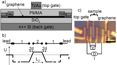
After exfoliation, thin graphite flakes were transferred onto a chip with 280 nm thermal oxide on top of an n++ Si substrate, used as the back gate. A single-layer graphene sheet was identified using an optical microscope, and 30 nm thick Ti/Au leads were evaporated onto the sheet using standard e-beam lithography. To form the dielectric layer for the top gate, a thin layer of PMMA (molecular mass 950K, 2% in anisole) was then spun onto the Si chip at 4000 rpm for 35 s and baked at for 2 minutes. On one section of the graphene sheet, the PMMA was cross-linked by exposure to 30 keV electrons at a dose of Zailer et al. (1996). The unexposed PMMA was removed by soaking the chip for 10 minutes in acetone. Finally, a 50 nm thick, 300 nm wide Ti/Au strip was deposited on top of the cross-linked PMMA using standard e-beam lithography to form the top gate (Fig. 1c.) Raman spectroscopy of the sheet indicates that it is in fact composed of a single layer Ferrari et al. (2006); Graf et al. (2007); EPAPS .
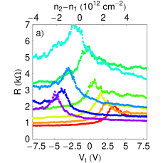
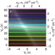
We performed conventional four-terminal current-biased lockin measurements (100 nA at 12.5 Hz) of the resistance of a PMMA-covered by section of a graphene flake, in which a potential barrier can be induced by the top gate (Fig. 1c). All the measurements were performed in liquid Helium at 4 K. In Fig. 2b, this resistance is plotted as a function of both the back gate voltage and the top gate voltage 111The leakage currents of back and top gates are linear in voltage over the full range studied, with leakage resistances and . Two clear white lines appear, indicating local maxima in the resistance in the different regions of the graphene sheet. In the bulk of the sheet (region 1), the average carrier density is given by , where the back gate capacitance per area is inferred from Hall measurements of other graphene flakes on the same oxide layer. The horizontal white line marks the neutrality point () in this region, allowing us to estimate . In region 2, the average density is modulated not only by the back gate, but also by the top gate, with capacitive coupling . The voltage is not necessarily zero, since the chemical doping in regions 1 and 2 can differ, and this difference can vary widely from sample to sample. The diagonal white line marks the neutrality point underneath the top gate (). The slope of this line provides the relative coupling of the graphene sheet to the two gates: , so . Using the PMMA thickness of 40 nm as measured by AFM, this value leads to a dielectric constant (close to the accepted room temperature value for non-cross-linked PMMA). The crossing point of these white lines yields EPAPS .
Transport fluctuations seen in Fig. 2 are a reproducible function of gate voltages and magnetic field (universal conductance fluctuations Rycerz et al. (2006)) with amplitude 222This value is measured by sweeping magnetic field at 17 values of the density between and .. The magnetoresistance is almost perfectly symmetric in magnetic field, as expected EPAPS . We extract the phase coherence length and the inter-valley scattering length from the weak localization peak. indicates that the sample is lying flat on the substrate EPAPS ; McCann et al. (2006); Morozov et al. (2006).
Fig. 2a shows selected cuts through Fig. 2b: device resistance across the potential barrier as a function of the top gate voltage , for several values of the bulk density . Each curve has a maximum close to , arising from the enhanced resistivity of the graphene in region 2. However, each curve is noticeably asymmetric with respect to this maximum: the resistance depends on whether or not the carriers in region 2 (electrons or holes) are the same type as those in region 1. Specifically, for given absolute values of the densities and , the resistance is always higher if the carrier types in the two regions are opposite () than if the carriers are the same throughout. In order to highlight the effects of pn junctions between regions 1 and 2, we extract for each value of the part of the resistance which depends on the sign of the carriers in region 2: , and (Fig. 3) 333The voltage at which the density is zero is determined using the above equation EPAPS .. The resistance of the device away from the junctions (region 1 and possibly the interior of region 2) does not depend on the sign of and hence is entirely contained in , which we do not examine further.
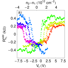
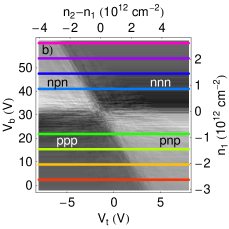
The presence of pn junctions between regions 1 and 2 is associated with a substantial increase of the overall resistance (white areas compared to black areas of Fig. 3b). We label each section of Fig. 3b with the carrier types in region 1 and 2, “p” for holes and “n” for electrons, to emphasize that enhanced resistance is associated with an npn or pnp junction. The junction-sensitive resistance curves are almost symmetric upon simultaneous sign change of both densities and : left-right reflection and color swap in Fig. 3a, or 180 degree rotation about the center in Fig. 3b. Deviations from this symmetry are presumably associated with uncontrolled spatial fluctuations in the density. Strikingly, a sharp step appears in the resistance as the boundary between nnn and npn or pnp configurations is crossed. We can explore the underlying physics of such a resistance increase in two opposite regimes: strongly diffusive or ballistic. Which applies to experiments depends on whether the elastic mean free path is greater than or less than the length over which the potential barrier rises.
In a simple model, the electrostatic potential induced by the set of two gates in the graphene sheet changes linearly between regions 1 and 2 over a width (Fig. 1b). Assuming perfect screening in the graphene sheet (a good approximation for our relevant density range), we estimate independent of carrier density, by solving the Laplace potential in the region between the top gate and the graphene. If the elastic mean free path is much shorter than , the total resistance can be estimated by integrating the local resistivity across the device. The conductivity at any position depends only on the density of charge carriers and can be inferred from resistance measurements where the density is uniform EPAPS . It can be approximated by an interpolation between low and high density behavior Geim and Novoselov (2007) where the mobility is and . Using and a width , we plot the predicted odd part of with respect to the voltage for each value of on Fig. 4a.

At high enough density, where the conductivity of graphene is proportional to the density of charges, one can define a mean free path in an isotropic diffusive model by , where is the effective Fermi wavevector defined relative to the K-point of the Brillouin zone 444Notice that the prefactor 2, which is related to the inverse of the dimension of the diffusive material in this model, might be a slight underestimate because of the angle-dependent scattering in graphene.. For , one can see in Fig. 2a that 555The conductivity can be estimated for as where is the resistance.. Therefore, for . The mean free path is then already of the order of for a few volts applied to the back gate. Hence, the diffusive model is a poor approximation and is unable to reproduce the data shown in Fig. 3.
The opposite regime of ballistic transport has been considered in the limits of sharp and smooth potential steps. We use here the results of Cheianov et al. Cheianov and Fal’ko (2006), which are valid in the limit . Note that the results for a sharp barrier Katsnelson et al. (2006) lead to the same qualitative results for but are more than 10 times smaller than what follows. The transmission probability for electrons impinging from region 1 on the interface between regions 1 and 2 depends strongly on the angle of incidence with respect to normal incidence, and is given by
| (1) |
We incorporate both interfaces of the potential barrier into the resistance calculation in the following way. In the fully ballistic regime (, where is the distance between the two interfaces), all possible reflections at the interfaces, and their interferences, must be taken into account. However, in the regime of this experiment, where , the two interfaces can be considered as independent resistors in series. Using a Landauer picture, the (antisymmetric) conductance through the full barrier is then
| (2) |
where we sum the transmission coefficients of incident modes having all possible values of the quantized wavevector component perpendicular to the interface , with integer and . Each such mode carries a conductance , where the degeneracy factor 4 is characteristic for graphene. The presence of two interfaces in series gives an overall prefactor of .
Using and , we plot the calculated odd part of the resistance in our ballistic model as a function of in Fig. 4b for the same densities as in the strongly diffusive case, assuming that the resistance in the case where the sign of is uniform is much smaller than . Although the results of the ballistic model are of the same order of magnitude as the measured values of the odd part of the resistance, the model is unable to reproduce some aspects of the experimental data. In particular, the model does not explain why does not only jump but continues to increase as passes beyond zero density. This behavior is particularly surprising as, for fixed , decreases with increasing . Furthermore, by construction, the model does not apply close to zero density or .
A complementary test of the unusual transmission through a potential barrier in graphene as a function of the angle of incidence was proposed by Cheianov et al. Cheianov and Fal’ko (2006). In the fully ballistic regime, the resistance across the barrier is predicted to increase as soon as a magnetic field applied perpendicular to the graphene sheet gets higher than a typical value , where is the barrier length ( via SEM). Using the values , , and , one gets .
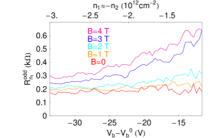
Fig. 5 shows measurements of the antisymmetrized resistance across the device for several values of a magnetic field applied perpendicular to the graphene sheet, with the top gate voltage adjusted to maintain . This odd part of the resistance shows an enhancement as the magnetic field increases above , an order of magnitude higher than the predicted transition field . The fully ballistic model is therefore unable to explain the results of our measurements in magnetic field. In fact, the diffusive model also predicts an increase of as increases, due to magnetoresistance of the strip near zero density between p and n regions. If the entire graphene sheet is set to zero density, its resistance increases with magnetic field similarly to at (Fig. 5). This qualitative agreement indicates that while ballistic physics plays a role in transport across the individual pn junctions, transport through the full npn barrier is far from ballistic.
In conclusion, we have fabricated a gate-tunable barrier device from a single-layer graphene sheet, and have hence created bipolar junctions within graphene. We study transport across the potential barrier as a function of Fermi level and barrier height, as well as in the presence of an external magnetic field, and demonstrate that a sharp increase in the resistance occurs as the potential crosses the Fermi level. This increase is better described by a ballistic than a diffusive model, but the dependence of the additional resistance as a function of the barrier height is not yet understood. A clear explanation of this behavior is essential for realizing many exciting proposed graphene electronics applications, such as electron focusing Cheianov et al. (2007).
We thank V.I. Fal’ko, E.A. Kim, D.P. Arovas and A. Yacoby for enlightening discussions, A. Geim for supplying the natural graphite and M. Brongersma, A. Guichard and E. Barnard for the Raman spectrometry. This work was supported by MARCO/FENA program and the Office of Naval Research. K.T. was supported by a Hertz Foundation graduate fellowship, N.S was supported by a William R. and Sara Hart Kimball Stanford Graduate Fellowship, J.A.S. by a National Science Foundation graduate fellowship. B.H. was supported in part by the Lavoisier fellowship. Work was performed in part at the Stanford Nanofabrication Facility of NNIN supported by the National Science Foundation under Grant ECS-9731293.
References
- Novoselov et al. (2004) K. S. Novoselov et al., Science 306, 666 (2004).
- Zhang et al. (2005) Y. Zhang, J. P. Small, M. E. S. Amori, and P. Kim, Phys. Rev. Lett. 94, 176803 (pages 4) (2005).
- Berger et al. (2004) C. Berger et al., J. Phys. Chem. B 108, 19912 (2004).
- Geim and Novoselov (2007) A. Geim and K. Novoselov, Nat. Mat. 6, 183 (2007).
- Ando et al. (1998) T. Ando, T. Nakanishi, and R. Saito, J. Phys. Soc. Jpn. 67, 2857 (1998).
- Katsnelson et al. (2006) M. I. Katsnelson, K. S. Novoselov, and A. K. Geim, Nat. Phys. 2, 620 (2006).
- Pereira et al. (2006) J. M. Pereira, V. Mlinar, F. M. Peeters, and P. Vasilopoulos, Phys. Rev. B 74, 045424 (2006).
- Cheianov and Fal’ko (2006) V. V. Cheianov and V. I. Fal’ko, Phys. Rev. B 74, 041403(R) (2006).
- (9) E. H. Hwang, S. Adam, and S. Das Sarma, Phys. Rev. Lett. 98, 186806 (2007) .A. Yacoby et al. (to be published)
- Zailer et al. (1996) I. Zailer et al., Semicond. Sci. Technol. 11, 1235 (1996).
- Ferrari et al. (2006) A. C. Ferrari et al., Phys. Rev. Lett. 97, 187401 (pages 4) (2006).
- Graf et al. (2007) D. Graf et al., Nano Lett. 7, 238 (2007).
- (13) See EPAPS Document No. E-PRLTAO-98-018724 for experimental details. For more information on EPAPS, see http://www.aip.org/pubservs/epaps.html.
- Rycerz et al. (2006) A. Rycerz, J. Tworzydlo, and C. Beenakker, arXiv:cond-mat/0612446v2 (2006).
- McCann et al. (2006) E. McCann et al., Phys. Rev. Lett. 97, 146805 (2006).
- Morozov et al. (2006) S.V. Morozov et al., Phys. Rev. Lett. 97, 016801 (2006).
- Cheianov et al. (2007) V. V. Cheianov, V. Fal’ko, and B. L. Altshuler, Science 315, 1252 (2007).