Energetics of positron states trapped at vacancies in solids
Abstract
We report a computational first-principles study of positron trapping at vacancy defects in metals and semiconductors. The main emphasis is on the energetics of the trapping process including the interplay between the positron state and the defect’s ionic structure and on the ensuing annihilation characteristics of the trapped state. For vacancies in covalent semiconductors the ion relaxation is a crucial part of the positron trapping process enabling the localization of the positron state. However, positron trapping does not strongly affect the characteristic features of the electronic structure, e.g., the ionization levels change only moderately. Also in the case of metal vacancies the positron-induced ion relaxation has a noticeable effect on the calculated positron lifetime and momentum distribution of annihilating electron-positron pairs.
pacs:
71.60.+z, 78.70.BjI Introduction
Positron annihilation spectroscopy Krause-Rehberg and Leipner (1999) is widely used in studying vacancy-type defects in metals and semiconductors. This is based on the fact that vacancies, in neutral or negative charge states, act as efficient positron traps due to the reduced repulsion of positive ions. Also the electron density is reduced at vacancies and by measuring the ensuing lifetime increase with respect to the delocalized positron bulk state one can estimate the extent of the open volume in defects. The momentum distribution of annihilating electron-positron pairs measured by Doppler broadening spectroscopy is at high momenta specific for the annihilating core electrons and thereby it enables the chemical identification of atoms surrounding vacancies.
For a given sample, the identification of the most abundant open-volume defect type, such as vacancy and vacancy agglomerates or vacancy-impurity complex, is based on the knowledge of the general behavior of positron annihilation results, i.e., on the information how the measured annihilation characteristics depend on the open volume or the chemical environment of defects. This knowledge has been acquired by measuring well-characterized reference samples including well-annealed (perfect bulk) materials as well as defected materials such as those containing monovacancies due to electron irradiation. Moreover, theoretical predictions of positron annihilation characteristics significantly support the defect identification. Puska and Nieminen (1994)
In order to interpret experimental results it is also important to understand the positron trapping process in detail. The trapping coefficient is an important quantity in determining defect concentrations. Its values have been estimated also theoretically for model systems by assuming that the positron gives in the trapping process its binding energy to excited electron-hole pairs or to phonons. Hodges (1970); Nieminen and Laakkonen (1979); Puska et al. (1990) In the present computational work our main theme is the effect of the positron on the ion lattice during the trapping process. Because the ion vibration frequency, which is of the order of the Debye phonon frequency, is much larger than the positron annihilation rate the ions around the defect have time prior to positron annihilation to relax to minimize the total energy of the defect-positron system. The ion relaxation affects the localization of the positron state and the annihilation characteristics. Below we argue using first-principles total-energy calculations that the positron-induced lattice relaxation is indispensable for the existence of localized positron states at vacancies in covalent semiconductors and thereby it completely determines the ensuing annihilation characteristics. In these systems, the strong influence of the positron is possible because the energy landscape as a function of the ion positions around the vacancy is very flat. Actually, the effect of the trapped positron is found so strong that it practically cancels the possible symmetry-lowering Jahn-Teller distortion of the vacancy. For vacancies in metals the influence of the trapped positron on the ion positions and especially on the energetics of the trapping process is smaller. However, the trapped positron causes a small increase in the open vacancy volume and thereby noticeable chances in the positron lifetime and in the momentum distribution of the annihilating pairs. It is important to note this from the modeling point of view.
In the case of semiconductors, positron annihilation has been used also to extract detailed information about the electronic structures of the defects, i.e., to determine the ionization levels of vacancy-type defects Corbel et al. (1988); Saarinen et al. (1991, 1993); LeBerre et al. (1995); Kuisma et al. (1997); Kauppinen et al. (1998); Arpiainen et al. (2002); Tuomisto et al. (2005) or just to probe the changes in their charge states. Mäkinen et al. (1992) In these experiments the charge state of the defect changes due to the thermal ionization or by illumination with light. The charge state change is then seen as a change in the positron lifetime reflecting electronic-structure-induced changes in the ion positions or as a dramatic change in the positron trapping rate when positive defects do not trap positrons. The question rising immediately in the first case is how much the positron-induced ionic relaxation affects the positions of the ionization levels by modifying or eventually breaking bonds between ions next to the vacancy. Our prediction is that although the changes in the ionic structure are rather large their effect on the ionization levels is minor.
Finally, we would like to point out that the comparison of calculated positron annihilation characteristics with the measured ones constitutes the fundamental test for theories describing electronic properties of materials and the positron-electron interactions as well as for many computational approximations. For delocalized positron states in perfect bulk solids there exist several systematic comparisons Puska and Nieminen (1983); Puska et al. (1989); Barbiellini et al. (1996); Makkonen et al. (2006) but for positron states trapped at vacancy defects comparisons treating several materials and systems on the same footing are scarce. The reason may be in difficulties arising in the theoretical description, e.g. in the density-functional theory Hohenberg and Kohn (1964); Kohn and Sham (1965) (DFT) the local-density approximation (LDA) for the electron exchange and correlation underestimates the energy band gap in semiconductors which may have severe consequences on the localized electron states and the ionic structure at defects. Moreover, the electron-positron correlation effects are known worse for localized positron states than for delocalized ones. Lastly, the broken translational symmetry leads to computational approximations such as the supercell method which requires large computer resources in order to show convergence of the results with respect to the supercell size. The aim of the present study is to remedy the situation by providing results for a representative set of materials. We consider metals with different lattice structures (close-packed Al, Cu, Mg, and body-centered-cubic Fe) and elemental (Si, Ge) and compound semiconductors (GaAs, GaN) with different degrees of bond ionicity. The structure of the present paper is as follows. In Sec. II we review shortly the theory and computational methods used. The results are given and described in Sec. III and they are discussed along comparisons with experimental results in Sec. IV. Section V presents our conclusions.
II Theory and computational details
II.1 Theoretical models
We perform first-principles electronic-structure calculations based on DFT for various vacancy defects in metals and in semiconductors. These calculations give the ionic positions by requiring that the total energy is minimized. This is equivalent to vanishing of the Hellman-Feynman forces on ions, calculated from the ground-state electron density. The trapped positron state at a defect can be included by generalizing to the two-component density-functional theory Boroński and Nieminen (1986) (2CDFT). For defects in semiconductors calculations optimizing the electronic and ionic structures as well as the positron density within the 2CDFT have appeared. Gilgien et al. (1994); Puska et al. (1995); Saito and Oshiyama (1996); Tang et al. (1997); Makhov and Lewis (2005)
In the present work we apply the so-called conventional scheme in which the localized positron density does not directly affect the average DFT electron density (the positron and its screening electron cloud form a neutral quasiparticle entering the system) and the positron state and annihilation characteristics are calculated in the LDA and at the zero-positron-density limit of the electron-positron correlation functionals. For example, this means that the potential entering the single-particle equation for the positron state reads as
| (1) |
where is the Coulomb potential due to electrons and nuclei, the electron density and is the electron-positron correlation energy Boroński and Nieminen (1986) for a positron in a homogeneous electron gas with density . It has been shown that the effects of the above two approximations largely cancel each other’s effects so that the conventional scheme and 2CDFT results for positron annihilation characteristics, for the total energy of the defect-positron system and for the positron trapping energy are very similar. Boroński and Nieminen (1986); Puska et al. (1995) Besides due to the conceptual simplification, we prefer the conventional scheme also because the 2CDFT functionals for finite positron densities are not accurately known.
When we relax the ions surrounding a defect with a trapped positron we minimize the total energy which in the conventional scheme is the sum of the DFT total energy for the electron-ion system and the positron energy eigenvalue. Thus, although our calculation is not a self-consistent 2CDFT calculation the positron state and the electron density are coupled via the ionic structure. In practice, we calculate the positron-induced Hellman-Feynman forces on ions using the so-called atomic superposition method (for details, see Ref. Makkonen et al., 2006).
The total annihilation rate which is the inverse of the positron lifetime is obtained from the overlap integral of the electron density and positron density
| (2) |
Above, is the enhancement factor for a positron a homogeneous electron gas Boroński and Nieminen (1986) with density , and and are the classical electron radius and the speed of light, respectively. We calculate the momentum distribution of the annihilating electron-positron pairs using the state-dependent enhancement scheme. Alatalo et al. (1996); Barbiellini et al. (1997) I.e.,
| (3) |
where and are the wave function and the state-dependent enhancement factor (in the LDA) for the electron state .
Besides the agreement with the 2CDFT the results obtained with the conventional scheme compare reasonably well also with experiment. Puska et al. (1995); Makkonen et al. (2006) First and foremost, the measured changes in the positron lifetime and in the relative changes in the core annihilation rate between the vacancy and bulk states are reproduced.
The most important aspect of the present work is the energetics of the defect-positron system. We define the positron trapping energy at a vacancy defect (the energy released in the trapping process) as the total energy difference between the systems of a defect and a delocalized positron and the same defect trapping a positron. Within the conventional scheme we obtain
| (4) | |||||
where is the total energy of the electron-ion system of the defect supercell without the localized positron, that with the localized positron. and are the energy eigenvalues of the positron in the delocalized bulk state and in the localized state at the vacancy, respectively. The last form in Eq. (4) shows that the trapping energy consists of the decrease of the positron energy eigenvalue and the increase in the (strain) energy stored in the ion lattice. In general, the Kohn-Sham eigenvalues in the 2CDFT have no physical meaning but as we have only one positron in the lattice and we use the conventional scheme the electron-positron interactions affect only the positron energy eigenvalue and the above analysis is justified.
The ionization level between the charge states and of a defect is defined as the position of the chemical potential relative to the top of the valence band so that the total energies of these two charge states are equal. I.e., we solve for in
| (5) |
where is the total energy of the supercell with the defect in the charge state and the term arises because electrons are added to () or taken from () the electron reservoir at the chemical potential level .
II.2 Calculation methods
In the supercell approach we use one has to take care of well-known artifacts. First, the energy eigenvalue of the delocalized positron in Eq. (4) and the valence band maximum in Eq. (5) are taken from the calculation for the perfect periodic bulk material. Because the energy zeroes differ between different supercells we align the effective potentials for the defect and bulk supercells far from the defect both in the case of electrons and the positron. Second, in order to avoid long-range Coulomb interactions between charged supercells in the superlattice we use a neutralizing uniform background charge. The unphysical energy terms due to the monopole-monopole interactions between the periodic images of the defects are corrected by the method by Makov and Payne. Makov and Payne (1995) However, in the case of defects in GaN we do not apply these corrections because they lead to an overcorrection. Since we are primarily interested not in the absolute values of the ionization levels but in their changes due to the localization of the positron the energy corrections are actually not of utmost importance.
Our computational methods are described in more detail in Ref. Makkonen et al., 2006 and here we will give only the main features. We perform electronic structure calculations within the LDA (Ref. Perdew and Zunger, 1981). The description of the electron-ion interaction is based on the projector augmented-wave (PAW) method Blöchl (1994) implemented in the plane-wave code vasp (Refs. Kresse and Furthmüller, 1996a, b; Kresse and Joubert, 1999). Using the PAW total charge density including the free atom core electrons the positron potential is constructed according to Eq. (1) and the lowest-energy positron state is calculated on a three-dimensional real-space point grid.
The lattice constants of the perfect bulk lattices are optimized and used in the defect calculations to define the supercell volume. For Si, Ge, and GaAs we use cubic 216-atom supercells. The Brillouin zone is sampled in the case of Si and GaAs using a Monkhorst-Pack (MP) point meshes Monkhorst and Pack (1976) whereas for Ge we use the -point sampling in order to avoid the artificial hybridization of the deep level and band states in the LDA (see Ref. Coutinho et al., 2006). Cutoff energies for Si, Ge, and GaAs are 246 eV, 270 eV, and 209 eV, respectively. We model wurtzite GaN using an orthorhombic 96-atom supercell, a MP -mesh and a cutoff energy of 400 eV. The hexagonal close-packed (hcp) Mg is modeled using an orthorhombic 48-atom supercell, a -mesh and the cutoff of 263 eV. For the body-centered cubic (bcc) Fe we calculate the magnetic ground states using a cubic 54-atom supercell, a MP -mesh and a cutoff energy of 268 eV. For defects in the face-centered cubic (fcc) metals Cu and Al we use cubic 108-atom supercells, a and MP -meshes and the cutoff energies of 342 eV and 301 eV, respectively.
III Results
III.1 Ion relaxation in positron trapping at vacancies
We study first the energetics of the trapping process, i.e., the interplay between the lowering of the positron energy eigenvalue and the energy stored in the strained lattice around the vacancy. Vacancies in Al and in Si represent two very different types of behaviors. In order to facilitate the scanning of the energy landscape when the ions relax due to the positron-induced forces we consider only the breathing-type ion relaxation. Thus, the point symmetries of the Al and Si vacancies are constrained to be and , respectively. The reaction coordinate is the relaxation of the nearest-neighbor ions of the vacancy from their ideal lattice positions. The positions of the other ions in the supercell are optimized.
The results for the Al vacancy are shown in Fig. 1(a). The energy of the electron-ion system (the uppermost curve) and the positron energy eigenvalue (the lowest curve) as well as their sum, the total energy of the system (the curve in the middle), are shown as a function of the relaxation of the nearest-neighbor ions. The energy zero is chosen to be the total energy of the vacancy and the trapped positron with ions relaxed without positron-induced forces. Then the uppermost curve corresponds also to the total energy of the vacancy and a delocalized positron. The smallest relaxation shown corresponds to the equilibrium ion positions of the Al vacancy without the trapped positron. The picture of the positron trapping process is clear. First, a fast (fast compared to the time scale of ionic movement) vertical Franck-Condon shift of the positron from the delocalized bulk state to the localized ground state at the vacancy takes place via electron-hole excitation [AB in Fig. 1(a)]. Then, the ions move slightly outward to minimize the total energy of the vacancy-positron system (BC). The escape of the positron from the trapped state via thermal processes, the so-called detrapping process, is very unlike due to large separation of two uppermost total energy curves.

The energetics for the neutral Si vacancy trapping a positron is depicted in Fig. 1(b). Actually, in this case we cannot find a bound positron state for the strongest inward relaxations and therefore the curves join at the leftmost point corresponding to the symmetric equilibrium relaxation without the trapped positron. At smaller inward relaxations a bound state exists and the positron energy eigenvalue decreases. Surprisingly, the energy stored in the electron-ion system and the lowering of the positron energy eigenvalue cancel each other rather accurately and the sum curve is very flat over a large range of ionic relaxation. The total energy shows a maximum and at small outward relaxations a minimum which gives a trapping energy [Eq. (4)] of 0.05 eV. In the trapping process a thermalized positron would “clear” a larger empty volume and a slightly deeper potential well for itself. In this way the trapping process is analogous to the self-trapping of electrons or holes in small polaron states in ionic crystals (see for example Ref. Mott and Stoneham, 1977). The flat total energy surface means that at finite temperatures the ions can be quite far from their absolute minimum energy configuration. However, the entropy contribution to the free energy would favor a larger open volume; The situation that all the four nearest-neighbor atoms are very close each other (strong inward relaxation) is very unlikely due to the small corresponding phase-space volume. As a consequence (assuming that positron detrapping is a vertical Franck-Condon process) there would also be a finite effective detrapping energy related to the distance between the two uppermost total energy curves in Fig. 1(b). The detrapping energy would be of the order of tenths of an eV.
In conclusion, the main characteristic differences between positron trapping at Al and Si vacancies are the much larger change in the positron energy eigenvalue for the Al vacancy and the much larger ion relaxation at the Si vacancy. The repulsive effect of the localized positron is stronger than one might expect on the basis of its small charge. The zero-point motion of the positron increases the force on the neighboring ions because the positron density penetrates closer to their nuclei. For example, we estimate that in the case of the Si vacancy the force due to a classical positive unit point charge at the center of the vacancy is only % of the force due to the localized positron. For the Al vacancy the symmetry persists also without constraints but for the neutral Si vacancy a symmetry lowering Jahn-Teller distortion is expected. In fact, when the defect is relaxed without a localized positron we find a Jahn-Teller distortion with the symmetry that lowers our calculated trapping energy slightly so that it even becomes negative. When the positron is trapped at the vacancy its repulsion practically restores the symmetry of the vacancy. Within the numerical accuracy we can consider the trapping energy to be practically zero. The flatness of the energy landscape will be a general characteristic feature of the Si vacancy trapping a positron.
III.2 Trapped positron states and annihilation at vacancies
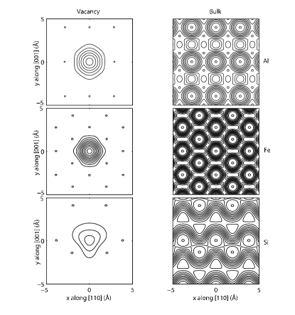
Next we present our first-principles results for various semiconductors and metals. Figure 2 shows the calculated positron densities at Al, Fe, and Si vacancies and in corresponding defect-free lattices. Thus, examples of fcc and bcc metals and tetrahedrally-bonded semiconductors are considered. The vacancies in metals localize the positron state effectively whereas in Si the positron density tends to leak along the open interstitial channels, which is reflected also in the smaller maximum value of the positron density. Because of the higher coordination number the Coulomb repulsion due to the nuclei is larger in the interstitial regions in the fcc and bcc lattices than in the open interstitial channels in the diamond structure of Si. Therefore the positron energy eigenvalue will decrease in the trapping process more in the fcc and bcc metals than in semiconductors
More quantitatively, we calculate positron trapping energies at vacancies and analyze how localized positrons affect the volumes and symmetries of the defects. Moreover, for vacancies in semiconductors we determine thermodynamical ionization levels in the energy band gap with and without a trapped positron. Our main results are presented in Table 1 and they are discussed in the following subsections.
III.2.1 Trapping energies
The positron trapping energies with components giving the lowering of the positron energy eigenvalue and the energy stored in the ion lattice are shown on the leftmost data columns in Table 1 [see the last form in Eq. (4)]. Several trends can be seen. First of all, the positron trapping energy at vacancies () in metals is typically clearly larger than that in semiconductors, i.e., the values for , , and are of the order of 2 eV whereas the values for and in GaAs are at most a few tenths of an eV. As can be seen in Table 1 this difference originates mainly from the fact that the lowering of the positron energy eigenvalue is larger in metals than in semiconductors. This in turn reflects the reduction of the positron-nucleus Coulomb repulsion which is larger when a vacancy is created in metal lattices with a larger atomic density and higher coordination number than in tetrahedrally coordinated semiconductor lattices with large open interstitial channels. However, there are exceptions from this general trend. Among the vacancies in metals, has a very low positron trapping energy which reflects the relatively low atom and electron densities. in GaN has a positron trapping energy similar to metals. This is no wonder because due to the size difference between the Ga and N atoms the Ga atom density in GaN is more than 60% of that in the Ga metal. The high atom density increases the positron-nucleus repulsion in the perfect GaN lattice and the lowering of the energy eigenvalue in trapping.
| Defect | (–1) | Symmetry | |||||||
|---|---|---|---|---|---|---|---|---|---|
| (eV) | (eV) | (eV) | (eV) | (%) | (ps) | ||||
| in Si | 0 | –0.17 | 0.69 | 0.86 | 0.47 (0.47) | +20.5 (–43.1) | () | 260 | 0.55 |
| –1 | –0.17 | 0.80 | 0.97 | +13.3 (–54.8)111Split vacancy. | ()11footnotemark: 1 | 255 | 0.57 | ||
| in Ge | 0 | (no minimum with bound e+) | (0.05) | (–42.5) | () | ||||
| –1 | (no minimum with bound e+) | (–45.3) | () | ||||||
| in GaAs | –2 | 0.39 | 0.75 | 0.36 | 0.74 (0.81) | –13.0 (–37.3) | () | 237 | 0.68 |
| –3 | 0.46 | 0.84 | 0.38 | –16.2 (–37.5) | () | 234 | 0.69 | ||
| in GaAs | 0 | (no minimum with bound e+) | (0.21) | (–41.1) | () | ||||
| –1 | (no minimum with bound e+) | (–51.1) | () | ||||||
| in GaN | –2 | 1.82 | 2.05 | 0.23 | 1.22 (1.43) | +59.0 (+29.7) | () | 216 | 0.57 |
| –3 | 2.04 | 2.28 | 0.24 | +60.7 (+29.4) | () | 216 | 0.55 | ||
| in GaN | 0 | (no bound e+ state) | (2.62) | (–7.7) | () | ||||
| –1 | (no bound e+ state) | (–19.5) | () | ||||||
| in bcc Fe | 1.67 | 2.34 | 0.67 | +8.4 (–6.2) | () | 159 | 0.75 | ||
| in hcp Mg | 0.34 | 0.49 | 0.15 | +6.3 (–2.9) | () | 289 | 0.56 | ||
| in fcc Cu | 2.20 | 2.58 | 0.38 | +7.4 (–3.8) | () | 163 | 0.74 | ||
| in fcc Al | 1.89 | 2.35 | 0.46 | +8.8 (–5.1) | () | 242 | 0.78 | ||
According to Table 1 the energy stored in to the lattice relaxation during the positron trapping process is of the same order of magnitude, eV. However, the crucial difference between typical metals and semiconductors is that for metals this energy is only a fraction of the energy which the positron gains in the lowering of the energy eigenvalue while for semiconductors it is of the same order of magnitude. Indeed, in the case of , and in GaAs the two components of the trapping energy nearly cancel each other.
Our calculations predict that the trapped positron state and the accompanying ionic relaxation at is only a metastable configuration and that the global energy minimum corresponds to an unperturbed vacancy and a delocalized positron. The energy barrier between these two minima is only some tenths of meV larger than the absolute value of the predicted negative trapping energy. The actual situation differs from that depicted in Fig. 1(b) because allowing the symmetry-breaking the Jahn-Teller effect lowers the energy of the vacancy relaxed without the trapped positron.
In the case of and in GaAs we find a bound positron state when the ions are frozen at ideal lattice positions or the nearest neighbor ions are relaxed outwards. But when we start optimizing the ion positions the vacancy relaxes strongly inward destroying the bound state. can be contrasted with ; The increase in the lattice constant from Si to Ge does not compensate the increase in the ion size and not even a metastable configuration with a bound positron state is found. For in GaN we did not found a bound positron state even when the ions neighboring the vacancy were frozen at positions corresponding to reasonable outward relaxations. In the latter case this can be explained by the small size of the N ion.
III.2.2 Defect geometries
The relative changes in the vacancy open volume are also given in Table 1. Here and refer to the volumes of the ideal (atoms at the ideal lattice sites) and relaxed vacancies, respectively. and are calculated as the volumes of polyhedra restricted by the nearest-neighbor atoms of the vacancy. The numbers in the parenthesis show that without trapped positrons vacancies in metals and in typical semiconductors have a tendency to shrink, i.e., the nearest neighbor atoms relax inward toward the center of the vacancy. The relaxation is large for semiconductors whereas in metals the ions remain close to their ideal lattice positions. In GaN the N atoms neighboring relax outward which reflects again the role of large Ga atoms in determining the lattice constant. The trapped positron increases the open volume. The effect is very dramatic in the case of semiconductors in which the volume increase of the vacancies is several tens of percents. For the neutral it is even of the order of 60%. The changes in the vacancy open volume are reflected in the positron lifetime and the momentum density of the annihilating electron-positron pairs (see Ref. Makkonen et al., 2006). The effect is strong also in the case of metals although the changes in the ionic relaxations are smaller.
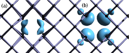
The strong effect of the trapped positron is seen also in the results for the vacancy point symmetry in semiconductors. Fig. 3(a) illustrates the case of the neutral . Without the trapped positron the Jahn-Teller effect lowers the point symmetry to and we see that the dangling bonds pointing toward the center of the vacancy hybridize to two pairs of bonds between the nearest-neighbor atoms. In Table 1 the symmetry of the plain singly negative is corresponding to the split-vacancy configuration where one of the atoms neighboring the vacancy relaxes so that a divacancy with an atom in the center results. These results for the Si vacancy are in good agreement with previous LDA results. Puska et al. (1998); Wright (2006) With a positron localized at the ideal lattice point symmetry is practically restored. As seen in Fig. 3(b) for the neutral the strong positron repulsion increases the distances and weakens the bonds between the nearest-neighbor atoms of the vacancy and the atoms end up at the ideal-lattice point-symmetry positions within the numerical accuracy. However, the deep localized electron state is not destroyed. This is the case also for the negative and there will be ionization levels in the band gap also when the vacancy traps a positron.
III.2.3 Ionization levels
The positions of the thermodynamic ionization levels for vacancies in semiconductors are also given in Table 1. Figure 4 shows as an example the determination of the level (–2/–3) for in GaAs without and with a trapped positron. The position of the ionization level is given by the point where the total energies cross. We see that the introduction of the positron lowers the thermodynamical ionization level. According to Table 1 the lowering of the ionization level due to positron trapping is a general trend which reflects the lowering of the positron energy eigenvalue at the vacancy due to the excess negative charge. Slightly surprisingly, the magnitude of the lowering is only of the order of 0.1 eV in spite of the rather large ion relaxations due to the trapped positron. The small change is due to the fact that the magnitudes of the ion relaxation in the adjacent charge states before or after the positron trapping are rather similar and because the excess electron density is rather delocalized and does not strongly lower the positron energy eigenvalue.

The behavior of the thermodynamic ionization levels in relation to the positron trapping is an important result justifying positron experiments devoted for determining ionization levels. Namely, we could think that the neutral and negatively charged states could become thermodynamically unstable with respect to loosing a bound electron when a positron is trapped. However, the lowering of the ionization levels indicates that this does not occur. Actually, within our model the trapped positron can then affect (lower) the measured ionization levels only in the case of the level and maybe also in the case of the level (–/–2). Namely, we expect that only the neutral or the singly negative charge state (not counting the charge of the localized positron) can trap an electron due to the positron-induced changes within the positron lifetime. The more negative charge states effectively repel free electrons hindering their trapping. The situation is similar to the positron trapping at positively charged vacancies. Puska et al. (1990) On the other hand, the ionization level between the positive and the neutral charge state is determined in the positron experiments by the fact that a positive defect does not trap a positron, and therefore the possible change of the vacancy charge state from the neutral to the negative one does not affect the determination of this level.
III.2.4 Positron annihilation characteristics
Positron lifetimes calculated for the different defects are also given in Table 1. The LDA for the electron-positron enhancement effects calculated with the Boroński-Nieminen interpolation form underestimates the positron lifetimes in comparison with experiment. The underestimation is especially strong for materials containing electrons such as transition metals and the III–V compound semiconductors such as GaN. Also the lattice constants calculated within the LDA for the electron exchange and correlation effects are too small compared with the measured ones decreasing the positron lifetimes. Therefore rather than the absolute lifetime values the differences or the ratios between the positron defect and bulk lifetimes are the most important figures. The ratios between the defect and bulk lifetimes are according to Table 1 about 1.1–1.25 and 1.5–1.8 for typical semiconductors and metals, respectively. For in GaN and for the ratios are 1.65 and 1.32, respectively. The ratios reflect the degree of the localization of the positron at the vacancies and, in general, their trends are similar to the trends in the positron trapping energies. It is interesting to note that the change of the charge state to a more negative one slightly decreases the positron lifetime in typical semiconductors whereas the lifetime in in GaN is insensitive to the charge state. The deep-level electron wave functions in in GaN are rather delocalized and adding more electrons on the deep levels does not appreciably change the total electron density and correspondingly the ionic relaxations.
Figure 5 shows ratio curves between the coincidence Doppler broadening momentum distributions of annihilating electron-positron pairs for vacancies and for the corresponding bulk lattices. The measured and calculated curves for triply-negative Ga vacancies in GaN and in GaAs are shown. The data correspond to the [0001] and [001] directions. The calculated distributions are convoluted with Gaussian functions with the full width at the half maximum of 5.3 and 5.5 for GaN and GaAs, respectively, corresponding to the experimental resolutions. The calculated curves quantitatively reproduce the experimental trends. At low momenta the ratio for GaN is higher than that for GaAs reflecting the larger reduction of the electron density at the vacancy in GaN. At high momenta the GaAs curve is above the GaN curve due the contribution of As 3d electrons in GaAs. The agreement at high momenta shows that our scheme is able to predict the overlap of the positron and core electron densities or at least the relative change in the positron-core electron overlap between the localized and delocalized positron states.

To enable further studies of trends between different materials Table 1 shows the relative parameters of vacancies, , that is an experimental parameter reflecting the decrease in core annihilation compared to the delocalized bulk state. Here is the parameter (integral over high-momentum part of the Doppler spectrum) corresponding to the localized defect state and that of the delocalized bulk state. The momentum window used is in all cases . The parameter reflects the positron localization and the extent of the high-momentum core electrons inside the vacancy. For example, it is interesting to note that the parameter is clearly smaller for Mg than for Al.
IV Discussion and comparison with experiment
Our model gives for vacancies in typical metals and for cation vacancies in compound semiconductors positron binding energies which are large enough that positron detrapping at elevated temperatures even near the melting point is unlikely. The predicted increases in the positron lifetimes in trapping are in agreement with experimental values. For example, for Al the calculated increase is 83 ps in agreement with the experimental one of 85 ps (Ref. Schaefer et al., 1986) and for for in GaN the calculated and measured increases are 85 and 75 ps (Ref. Hautakangas et al., 2006), respectively. The calculated and measured electron-positron momentum distributions at high momenta also show a good correspondence (Fig. 5 gives an example) meaning that our model is able to reproduce the positron overlap with ion cores in a reasonable manner.
The agreement between theory and experiment becomes less clear when the predicted positron trapping energy decreases. In the case of positron trapping at vacancies in Mg the calculated positron lifetime increase is from 219 ps to 289 ps whereas the much smaller increase from 225 ps to 255 ps has been measured between well a annealed sample and a sample with thermally generated vacancies. Hautojärvi et al. (1982) The calculated large lifetime increase is also reflected in a rather small parameter of 0.56 for . However, the calculated positron trapping energy of 0.34 eV is in agreement with the estimate of eV by Hautojärvi et al. Hautojärvi et al. (1982) One possible source of the theory-experiment disagreement could be difficulties in extracting bulk and vacancy lifetimes for Mg in measurements.
Our calculations predict a vanishingly small positron trapping energy at vacancies in Si, of the order of thermal energy at room temperature. The trapped positron state does not exist when the vacancy is relaxed without the influence of the localized positron, which in principle prevents positron trapping at the vacancy at zero temperature. Our result is, however, even qualitatively wrong since the predicted trapping energy is negative. However, the behavior of during positron trapping is unique reflecting the very flat energy landscape the ions feel around the vacancy. The flatness is due to the different competing possibilities for bonding and rebonding in a covalent material. The flat energy landscape is also behind the scatter of the DFT results for the structure and energetics of the Si vacancy. Only recently, when calculations with very large supercells (up to 1000 Si atoms) have become possible the results show a satisfactory numerical convergence. Wright (2006) Figure 1(b) shows that the energy landscape of the Si vacancy with a trapped positron is even flatter than that of the plain vacancy. This means, as discussed above, that the entropy contribution should be taken into account when describing the trapped state at finite temperatures. However, one should bear in mind that the errors arising, e.g., from the LDA’s for the electron-positron correlation energy and for the electron-electron exchange and correlation may be of the order of tenths of an eV. For example, the scatter in the calculated formation energies for is of this order or even larger. Thus, our scheme may describe even qualitatively incorrectly the actual positron trapping process in borderline cases such as .
The flat energy landscape for would introduce strong temperature-dependence to positron trapping and detrapping processes. In our model [Fig. 1(b)] the positron trapping would, in principle, be possible at finite temperatures because part of the time the vacancy volume is so large that a bound positron state exists. This probability is, however, strongly temperature-dependent and in the experiments the trapping rate as a function of temperature is seen to be rather constant except for the case of negative defects for which the trapping rate decreases with increasing temperature. Puska et al. (1990)
The concept of positron binding energy seems to be a difficult one to define or at least it is difficult to get a quantitative agreement between experiment and theory even if the computational results were exact. First of all, one of the assumptions behind the relation between trapping and detrapping rates Manninen and Nieminen (1981) typically used in the interpretation of experimental data is that the excitations of the positron are decoupled from the excitations of the system. According to our calculation this clearly is not the case. Secondly, the positron detrapping energy (the threshold energy needed to detrap a localized positron) in the case of strongly depends on the detrapping mechanism (fast vertical transition vs slow transition due to phonons) and on the ionic structure of the defect at the instant of detrapping [see Fig. 1(b)]. In the case of this kind of an energy landscape it is difficult to draw conclusions about the actual positron trapping and detrapping processes. According to our calculations the strain energy stored in the relaxation of the vacancy is so large that all the released energy can be stored in it (analogously to the trapping of a small polaron). However, although the energy is conserved between the initial and final states the differing time scales in electronic (transition of the positron from delocalized to localized state) and ionic processes (relaxation of the vacancy during positron trapping) complicate the picture. Although our results may not in all cases be even qualitatively correct they clearly suggest that the models for positron trapping in semiconductors Puska et al. (1990) need refinement.
Recent measurements of heavily As-doped Si indicate that positron trapping energies at vacancy defects in highly As-doped Si may be low and thermal detrapping is possible. Kuitunen et al. (2007) Namely Kuitunen et al. found that positron detrapping happens from the Si vacancy decorated by three As atoms () at temperatures above 500 K. For vacancies decorated with one or two As atoms they did not notice positron detrapping. Using the relation between the detrapping and trapping rates derived by Manninen and Nieminen Manninen and Nieminen (1981) Kuitunen et al. determined for the trapping energy of 0.27 eV. Our scheme gives a clearly smaller positron trapping energy of 0.06–0.1 eV for . Similarly to the case of we do not find for and an energetically favored trapped positron state but just a metastable configuration in disagreement with the experimental trend. The trend in our trapping energies is exactly the opposite; the trapping energy increases with the increasing number of As atoms (). This is because the large As ions around the vacancy do not relax inwards as strongly as the neighboring Si ions so that the energy stored in the ionic lattice in the positron trapping process is smaller for the As decorated vacancy than for the clean vacancy. A well-known shallow positron trap in Si with open volume is the complex formed by a vacancy and an interstitial oxygen. For it, the reported positron binding energies are of the order of 40–50 meV (Refs. Polity et al., 1998; Kauppinen et al., 1998). The open volume of the complex is so small (see Ref. Pesola et al., 1999) that we do not expect it to trap positrons in our calculations.
The fact that a bound positron state can be found at or at in GaAs when freezing the ions at ideal positions means that the bound positron states are very close to appear, and an improvement in the theoretical description could lead to bound positron states also for optimized ion positions. In experimental works Polity and Rudolf (1999); Würschum et al. (1989); Moser et al. (1985) positron lifetime components between 279 and 292 ps are assigned to . The measured lifetimes can be contrasted to the measured bulk lifetime of 228 ps (Ref. Polity and Rudolf, 1999). These vacancy lifetimes are already quite close to the theoretical estimate of 316 ps for an ideal divacancy in Ge (the corresponding bulk lifetime is 229 ps). Puska et al. (1989) For an ideal neutral monovacancy we get the lifetime of 246 ps which is only 33 ps longer than our bulk lifetime. These comparisons suggest that the experimentally observed lifetime components are too long to be explained by annihilation at ideal monovacancy-size defects. Measurements Saarinen et al. (1991) for -type GaAs show the lifetimes of 257 ps and 295 ps (the experimental bulk lifetime is 231 ps). These were assigned to negative and neutral As vacancies possibly associated with impurity atoms on the basis of measured ionization levels and corresponding old computational results Puska (1989); Xu and Lindefelt (1990) which suggested that the levels of are near the conduction band. The measurements gave ionization levels of = – 0.140 eV and = – 0.030 eV, where is the conductance band minimum. Our first-principles results, which are in accordance with those in Ref. El-Mellouhi and Mousseau, 2005, indicate that these ionization levels of clean in GaAs are close to the top of the valence band. This supports also the conclusions that the defects observed in positron measurements are not clean vacancies.
Finally, our calculations for in GaN suggest that bound positron states at small anion vacancies in compound semiconductors are not possible. This should be contrasted with a positron annihilation study in which the detection of N vacancies is reported. Hautakangas et al. (2003) In the interpretation, however, the short lifetime component is associated with -impurity complexes and not with isolated .
V Conclusions
We have studied, using first-principles calculations, the role of lattice relaxations around vacancies in the positron trapping process in various metals and semiconductors. In metals the trapping energies are typically of the order of 1…2 eV. The lattice relaxes due to the trapped positron and the positron annihilation parameters change but especially the qualitative effects are small. The most important difference between typical metals and semiconductors is the magnitude of the strain energy stored in the lattice compared to the lowering of the positron energy eigenvalue. For semiconductors these two can be of the same order of magnitude because of the smaller reduction of nucleus repulsion in the trapping process. This leads to rather small values for the trapping energy.
In the case of covalently bonded elemental semiconductors such as Si and Ge the energy landscape of the positron-vacancy system is extremely flat which suggests that entropic considerations have to be taken into account when discussing the ionic structure of the vacancy with a localized positron at finite temperatures. For Si the calculations give, in disagreement with experiments, vanishingly small or rather sightly negative trapping energies suggesting that trapping of thermalized positrons would not even be energetically favorable.
Also the vacancy in Ge and anion vacancies in compound semiconductors are challenging tests for theoretical methods since in the calculations there is either no bound positron state at the vacancy or the trapping is energetically unfavorable and there is no local energy minimum configuration at which the positron is trapped at the vacancy. Furthermore, for the vacancy in Si the configuration with the trapped positron is just a metastable state while in the ground state the positron is in the delocalized bulk state. An interesting finding is that a localized positron cancels all the Jahn-Teller distortions we observed when having no positron at the vacancy.
In general, the higher the predicted positron trapping energy is the better is the agreement between our results and experiments. However, also in the case of defects in Si we get a surprisingly good agreement in calculated lifetimes and Doppler broadening spectra for the metastable state.
We have also studied the effect of the localized positron on the electronic structure of the vacancies in semiconductors by evaluating thermodynamical ionization levels of vacancies. The positron-induced changes are usually only of the order of 0.1 eV. In general, the levels move closer to the valence band maximum. A positron-induced change in the defect charge state in this model is likely only in the case of a neutral defect since positive ones do not trap positrons and negative ones electrons within the lifetime of the trapped positron.
Acknowledgements.
We are grateful for discussions with Academy Prof. R. M. Nieminen and Dr. F. Tuomisto. We also acknowledge the generous computer resources from the Center of Scientific Computing, Espoo, Finland. I.M. acknowledges the financial support by the Finnish Academy of Science and Letters, Vilho, Yrjö, and Kalle Väisälä Foundation.References
- Krause-Rehberg and Leipner (1999) R. Krause-Rehberg and H. Leipner, Positron Annihilation in Semiconductors (Springer-Verlag, Berlin, 1999).
- Puska and Nieminen (1994) M. J. Puska and R. M. Nieminen, Rev. Mod. Phys. 66, 841 (1994).
- Hodges (1970) C. H. Hodges, Phys. Rev. Lett. 25, 284 (1970).
- Nieminen and Laakkonen (1979) R. M. Nieminen and J. Laakkonen, Appl. Phys 20, 181 (1979).
- Puska et al. (1990) M. J. Puska, C. Corbel, and R. M. Nieminen, Phys. Rev. B 41, 9980 (1990).
- Corbel et al. (1988) C. Corbel, M. Stucky, P. Hautojärvi, K. Saarinen, and P. Moser, Phys. Rev. B 38, 8192 (1988).
- Saarinen et al. (1991) K. Saarinen, P. Hautojärvi, P. Lanki, and C. Corbel, Phys. Rev. B 44, 10585 (1991).
- Saarinen et al. (1993) K. Saarinen, S. Kuisma, P. Hautojärvi, C. Corbel, and C. LeBerre, Phys. Rev. Lett. 70, 2794 (1993).
- LeBerre et al. (1995) C. LeBerre, C. Corbel, R. Mih, M. R. Brosel, S. Tüzemen, S. Kuisma, K. Saarinen, P. Hautojärvi, and R. Fornari, Appl. Phys. Lett. 66, 2534 (1995).
- Kuisma et al. (1997) S. Kuisma, K. Saarinen, P. Hautojärvi, and C. Corbel, Phys. Rev. B 55, 9609 (1997).
- Kauppinen et al. (1998) H. Kauppinen, C. Corbel, J. Nissilä, K. Saarinen, and P. Hautojärvi, Phys. Rev. B 57, 12911 (1998).
- Arpiainen et al. (2002) S. Arpiainen, K. Saarinen, P. Hautojärvi, L. Henry, M.-F. Barthe, and C. Corbel, Phys. Rev. B 66, 075206 (2002).
- Tuomisto et al. (2005) F. Tuomisto, K. Saarinen, D. C. Look, and G. C. Farlow, Phys. Rev. B 72, 085206 (2005).
- Mäkinen et al. (1992) J. Mäkinen, P. Hautojärvi, and C. Corbel, J. Phys.: Condens. Matter 4, 5137 (1992).
- Puska and Nieminen (1983) M. J. Puska and R. M. Nieminen, J. Phys. F 13, 333 (1983).
- Puska et al. (1989) M. J. Puska, S. Mäkinen, M. Manninen, and R. M. Nieminen, Phys. Rev. B 39, 7666 (1989).
- Barbiellini et al. (1996) B. Barbiellini, M. J. Puska, T. Korhonen, A. Harju, T. Torsti, and R. M. Nieminen, Phys Rev. B 53, 16201 (1996).
- Makkonen et al. (2006) I. Makkonen, M. Hakala, and M. J. Puska, Phys. Rev. B 73, 035103 (2006).
- Hohenberg and Kohn (1964) P. Hohenberg and W. Kohn, Phys. Rev. 136, B864 (1964).
- Kohn and Sham (1965) W. Kohn and J. Sham, Phys. Rev. 140, A1133 (1965).
- Boroński and Nieminen (1986) E. Boroński and R. M. Nieminen, Phys. Rev. B 34, 3820 (1986).
- Gilgien et al. (1994) L. Gilgien, G. Galli, F. Gygi, and R. Car, Phys. Rev. Lett. 72, 3214 (1994).
- Puska et al. (1995) M. J. Puska, A. P. Seitsonen, and R. M. Nieminen, Phys. Rev. B 52, 10947 (1995).
- Saito and Oshiyama (1996) M. Saito and A. Oshiyama, Phys. Rev. B 53, 7810 (1996).
- Tang et al. (1997) Z. Tang, M. Hasegawa, T. Chiba, M. Saito, A. Kawasuso, Z. Q. Li, R. T. Fu, T. Akahane, Y. Kawazoe, and S. Yamaguchi, Phys. Rev. Lett. 78, 2236 (1997).
- Makhov and Lewis (2005) D. V. Makhov and L. J. Lewis, Phys. Rev. B 71, 205215 (2005).
- Alatalo et al. (1996) M. Alatalo, B. Barbiellini, M. Hakala, H. Kauppinen, T. Korhonen, M. J. Puska, K. Saarinen, P. Hautojärvi, and R. M. Nieminen, Phys. Rev. B 54, 2397 (1996).
- Barbiellini et al. (1997) B. Barbiellini, M. Hakala, M. J. Puska, R. M. Nieminen, and A. A. Manuel, Phys. Rev. B 56, 7136 (1997).
- Makov and Payne (1995) G. Makov and M. C. Payne, Phys. Rev. B 51, 4014 (1995).
- Perdew and Zunger (1981) J. P. Perdew and A. Zunger, Phys. Rev. B 23, 5048 (1981).
- Blöchl (1994) P. E. Blöchl, Phys. Rev. B 50, 17953 (1994).
- Kresse and Furthmüller (1996a) G. Kresse and J. Furthmüller, Comput. Mat. Sci. 6, 15 (1996a).
- Kresse and Furthmüller (1996b) G. Kresse and J. Furthmüller, Phys. Rev. B 54, 11169 (1996b).
- Kresse and Joubert (1999) G. Kresse and D. Joubert, Phys. Rev. B 59, 1758 (1999).
- Monkhorst and Pack (1976) H. J. Monkhorst and J. D. Pack, Phys. Rev. B 13, 5188 (1976).
- Coutinho et al. (2006) J. Coutinho, S. Öberg, V. J. B. Torres, M. Barroso, R. Jones, and P. R. Briddon, Phys. Rev. B 73, 235213 (2006).
- Mott and Stoneham (1977) N. F. Mott and A. M. Stoneham, J. Phys. C 10, 3391 (1977).
- Puska et al. (1998) M. J. Puska, S. Pöykkö, M. Pesola, and R. M. Nieminen, Phys. Rev. B 58, 1318 (1998).
- Wright (2006) A. F. Wright, Phys. Rev. B 74, 165116 (2006).
- Hautakangas et al. (2006) S. Hautakangas, I. Makkonen, V. Ranki, M. J. Puska, K. Saarinen, X. Xu, and D. C. Look, Phys. Rev. B 73, 193301 (2006).
- Laine et al. (1996) T. Laine, K. Saarinen, J. Mäkinen, P. Hautojärvi, C. Corbel, L. N. Pfeiffer, and P. H. Citrin, Phys. Rev. B 54, R11050 (1996).
- Schaefer et al. (1986) H. E. Schaefer, W. Stuck, F. Banhart, and W. Bauer, in Proceedings of the 8th International Conference on Vacancies and Interstitials in Metals and Alloys, edited by C. Ambromeit and H. Wollenberger (Trans Tech, Aedermannsdorf, 1986).
- Hautojärvi et al. (1982) P. Hautojärvi, J. Johansson, A. Vehanen, J. Yli-Kauppila, J. Hillairet, and P. Tzanétakis, Appl. Phys. A 27, 49 (1982).
- Manninen and Nieminen (1981) M. Manninen and R. M. Nieminen, Appl. Phys A 26, 93 (1981).
- Kuitunen et al. (2007) K. Kuitunen, K. Saarinen, and F. Tuomisto, Phys. Rev. B 75, 045210 (2007).
- Polity et al. (1998) A. Polity, F. Börner, S. Huth, S. Eichler, and R. Krause-Rehberg, Phys. Rev. B 58, 10363 (1998).
- Pesola et al. (1999) M. Pesola, J. von Boehm, T. Mattila, and R. M. Nieminen, Phys. Rev. B 60, 11449 (1999).
- Polity and Rudolf (1999) A. Polity and F. Rudolf, Phys. Rev. B 59, 10025 (1999).
- Würschum et al. (1989) R. Würschum, W. Bauer, K. Maier, A. Seeger, and H.-E. Schaefer, J. Phys.: Condens. Matter 1, 33 (1989).
- Moser et al. (1985) P. Moser, J. L. Pautrat, C. Corbel, and P. Hautojärvi, in Positron annihilation, edited by P. C. Jain, R. M. Singru, and P. Gopinathan (World Scientific, Singapore, 1985).
- Puska (1989) M. J. Puska, J. Phys.: Condens. Matter 1, 7347 (1989).
- Xu and Lindefelt (1990) H. Xu and U. Lindefelt, Phys. Rev. B 41, 5979 (1990).
- El-Mellouhi and Mousseau (2005) F. El-Mellouhi and N. Mousseau, Phys. Rev. B 71, 125207 (2005).
- Hautakangas et al. (2003) S. Hautakangas, J. Oila, M. Alatalo, K. Saarinen, L. Liszkay, D. Seghier, and H. P. Gislason, Phys. Rev. Lett. 90, 137402 (2003).