Substrate-induced bandgap in graphene on hexagonal boron nitride
Abstract
We determine the electronic structure of a graphene sheet on top of a lattice-matched hexagonal boron nitride (h-BN) substrate using ab initio density functional calculations. The most stable configuration has one carbon atom on top of a boron atom, the other centered above a BN ring. The resulting inequivalence of the two carbon sites leads to the opening of a gap of 53 meV at the Dirac points of graphene and to finite masses for the Dirac fermions. Alternative orientations of the graphene sheet on the BN substrate generate similar band gaps and masses. The band gap induced by the BN surface can greatly improve room temperature pinch-off characteristics of graphene-based field effect transistors.
pacs:
71.20.-b, 73.22.-f, 73.20.-rIntroduction Less than 3 years ago it was discovered that graphene – a one-atom-thick carbon sheet – can be deposited on a silicon-oxide surface by micromechnical cleavage of high quality graphite Novoselov et al. (2004). The graphene flakes are micrometers in size, sufficiently large to have contacts attached so as to construct field effect transistors (FETs). Electrical transport measurements made clear that at room temperature graphene has an electron mobility of at least 10 000 , a value ten times higher than the mobility of silicon wafers used in microprocessors Novoselov et al. (2004, 2005); Zhang et al. (2005). The high mobility is not much affected by a field-induced excess of electrons or holes.
A graphene sheet has a honeycomb structure with two crystallographically equivalent atoms in its primitive unit cell. Two bands with character belonging to different irreducible representations cross precisely at the Fermi energy at the and points in momentum space. As a result undoped graphene is a zero-gap semiconductor. The linear dispersion of the bands results in quasiparticles with zero mass, so-called Dirac fermions. At energies close to the degeneracy point the electronic states form perfect Dirac cones. The absence of a gap, preventing the Dirac fermions from attaining a finite mass and complicating the use of graphene in electronic devices Geim and Novoselov (2007), is related to the equivalence of the two carbon sublattices of graphene.
The relativistic nature of the Dirac fermions gives rise to counterintuitive phenomena. One, known as the Klein paradox, is that relativistic electrons exhibit perfect transmission through arbitrarily high and wide potential barriers. This effect is related to an unwanted characteristic of graphene FETs, namely that pinch-off is far from complete Katsnelson et al. (2006). If one applies a gate voltage so that either holes or electrons are injected into the graphene sheet, the FET is open and its conductivity high. One can then try to block the current by tuning the gate voltage to move the graphene layer towards the charge neutrality point where the Fermi energy coincides with the Dirac points; at this energy the density of states vanishes and nominally there are no carriers present. However, it turns out that in spite of the lack of electronic states the conductivity does not vanish in this case. Rather, it assumes the minimal value , where is Planck’s constant and the unit of charge. Thus even when pinched-off to its maximum the FET still supports an appreciable electrical current, which is intrinsic to graphene and related to the fact that the Dirac fermions are massless Novoselov et al. (2005); Zhang et al. (2005); Katsnelson et al. (2006); Geim and Novoselov (2007); Heersche et al. (2007); van den Brink (2007).
Inducing a gap The poor pinch-off can only be remedied by generating a mass for the Dirac fermions. A number of possibilities exist to do so. One is to use bi-layer graphene which will have a gap if the top and bottom layers are made inequivalent, for instance by applying a bias potential Katsnelson et al. (2006). Another is the use of graphene nanoribbons, where gaps arise from the lateral constriction of the electrons in the ribbon. The size of the gap then depends on the detailed structure of the ribbon edges Son et al. (2006); Han et al. (2007); Z. Chen et al. (2007). We investigate an alternative possibility and consider graphene on a substrate that makes the two carbon sublattices inequivalent. This breaks the sublattice symmetry directly, generating an intrinsic and robust mass for the Dirac fermions.
As a substrate, hexagonal boron nitride (h-BN) is a suitable choice Suenaga et al. (1997). This wide gap insulator has a layered structure very similar to that of graphene but the two atoms in the unit cell are chemically inequivalent. Placed on top of h-BN the two carbon sublattices of graphene become inequivalent as a result of the interaction with the substrate. Our band structure calculations in the local-density approximation show that a gap of at least 53 meV – an energy roughly twice as large as at room temperature – is induced. This can be compared to graphene on a copper metallic surface where the gap is found to be much smaller and can even vanish, depending on the orientation of the graphene sheet.

Stable structure The lattice mismatch of graphene with hexagonal boron nitride is less than 2%. Just as in graphite, the interaction between adjacent BN layers is weak. The h-BN layers have an stacking: the boron atoms in layer are directly above the nitrogen atoms in layer . Within the local density approximation (LDA) the minimum energy separation of adjacent layers is found to be 3.24 Å, which is reasonably close to the experimental value of 3.33 Å. Because generalized gradient approximation (GGA) calculations give essentially no bonding between BN planes and lead to excessively large values of Kern et al. (1999), we opt for electronic structure calculations within the LDA. Electronically, h-BN is a wide gap insulator, with experimentally a gap of 5.97 eV Watanabe et al. (2004). This gap is underestimated by about in LDA. A quasi-particle correction on top of the LDA brings it into very close agreement with experiment Blase et al. (1995); Arnaud et al. (2006) and reinterprets experiment in terms of an indirect gap. For the composite graphene layer on top of h-BN system, we use the LDA lattice parameter for graphene, Å.

On the basis of this structural information we construct a unit cell
with 4 layers of h-BN and a graphene top layer. We represent the vacuum
above graphene with an empty space of 12 to 15 Å. The results to be
presented below converge quickly as a function of the number of h-BN
layers and the width of the vacuum space, consistent with weak interlayer
interactions. No significant difference in the final results were found
when 6 layers of h-BN were used. The in-plane periodicity is that of a
single graphene sheet with a hexagonal unit cell containing two carbon
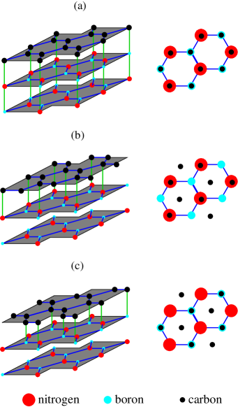
atoms. We consider three inequivalent orientations of the graphene sheet
with respect to the h-BN, see Fig. 1:
- the configuration with one carbon over B, the other carbon over N.
- the configuration with one carbon over N, the other carbon
centered above a h-BN hexagon.
- the configuration with one carbon over B, the other carbon centered
above a h-BN hexagon.
The self-consistent calculations were performed with the Vienna Ab-initio Simulation Package (VASP) Kresse and Furthmuller (1996a, b) using a plane wave basis and a kinetic energy cutoff of 600 eV. The Brillouin Zone (BZ) summations were carried out with the tetrahedron method and a grid which included the , and points. A dipole correction avoids interactions between periodic images of the slab along the -direction Neugebauer and Scheffler (1992).
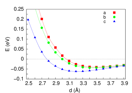
The total energies of the three configurations are shown as a function of the distance between the h-BN surface and the graphene sheet in Fig. 2. For all distances, the lowest-energy configuration is with one carbon on top of a boron atom and the other above a h-BN ring. The equilibrium separation of 3.22 Å for configuration is smaller than 3.50 Å for configuration and 3.40 Å for configuration . For all three configurations the energy landscape is seen to be very flat around the energy minimum. Though symmetry does not require inequivalent carbon atoms to be equidistant from the BN layer, in practice the stiffness of the graphene sheet prevents any significant buckling.

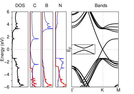
Band structure With the stable structures in hand, we compute the corresponding electronic band structures and projected densities of states which are shown in Fig. 3 for configuration . For the h-BN derived bands a gap of 4.7 eV at the -point is found, which is nearly identical to the LDA gap value at this particular point in the Brillouin zone found for bulk h-BN Arnaud et al. (2006). Within this boron nitride gap, the bands have entirely carbon character as expected on the basis of the weak interlayer interactions in both bulk h-BN and graphite. On the electron-volt scale of Fig. 3 the Dirac cone around the -point appears to be preserved. However, zooming in on that point in the BZ (see inset) reveals that a gap of 53 meV is opened and the dispersion around the Dirac points is quadratic.
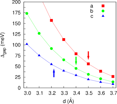
The band gaps for the three different configurations are shown in Fig. 4 as a function of the distance between the graphene sheet and the h-BN surface. Decreasing this distance increases the gap, as expected for a physical picture based upon a symmetry-breaking substrate potential. The band gaps that are opened at the equilibrium geometries of the and configurations are 56 meV and 46 meV, respectively, which are comparable to the band gap obtained for configuration . The largest gap is found for the configuration with one carbon atom above a boron atom and the other above a nitrogen atom. Again, this is expected for gap opening induced by breaking the symmetry of the two carbon atoms. Since LDA generally underestimates the gap, the values that we obtain put a lower bound on the induced band gaps, which we thus find to be significantly larger than at room temperature.

Although the lattice mismatch between graphene and h-BN constants is less than 2% and can be neglected in a first approximation, in a real system incommensurability will occur and we expect the strong in-plane bonding of both graphene and h-BN to prevail over the weak inter-plane bonding. For graphene on Ir(111) where the lattice mismatch is , Moiré patterns have been observed in STM images N’Diaye et al. (2006). There, first-principles calculations showed that regions could be identified where the graphene was in registry with the underlying substrate in high symmetry configurations analogous to the , and configurations discussed above, and transition regions with little or no symmetry N’Diaye et al. (2006). The graphene separation from the substrate varied across the surface leading to bending of the graphene sheet. If we could take the lattice mismatch into account in a large supercell in a similar fashion, some areas of graphene would be forced into the higher energy and configurations with larger separations to the BN substrate. However, the corresponding band gaps are all of the order of the 50 meV we find for the lowest energy configuration, or higher. It seems reasonable to conclude that the broadening resulting from lattice mismatch will not reduce the gap substantially.
Cu(111) substrate The situation changes markedly for graphene on a Cu(111) surface. The copper surface layer forms a triangular lattice, matching that of graphene to better than 4%. We consider two configurations of graphene on Cu(111). Either the center of each carbon hexagon is on top of a Cu atom, which we call the symmetric configuration in the following, or every second carbon atom is on top of a Cu atom, which we call the asymmetric configuration. For the asymmetric and symmetric configurations, LDA calculations yield equilibrium separations of Å and Å which are comparable to those of graphene on h-BN (Fig. 2). The total energy difference between the two configurations is only about meV. In the asymmetric configuration a small gap of meV is opened in the graphene band structure, whereas in the symmetric configuration the gap remains very close to zero. In both cases we find very little mixing between copper and carbon states. The difference between the gaps can be explained by the fact that the symmetric configuration preserves the graphene symmetry in the top Cu surface layer, whereas the symmetry is broken in the asymmetric configuration. The effect of this symmetry breaking is small, however, and the resulting band gap is much smaller than that induced by h-BN and comparable to the typical thermal broadening reported in experiments Novoselov et al. (2005); Geim and Novoselov (2007). Taking into account the graphene-Cu lattice mismatch in for instance a super cell calculation N’Diaye et al. (2006) will not to change this conclusion.
For both configurations of graphene on Cu, a charge rearrangement at the interface is found which moves the Fermi level away from the induced gap Giovannetti et Al (2007) by much more than the magnitude of the gap itself. This is in contrast to a h-BN substrate, where the Fermi level remains in the induced gap. Around the Fermi level of graphene on Cu the band dispersion is still linear. Consequently, the properties characteristic of graphene which result from the linear dispersion should be preserved. In for instance tunneling experiments that require adsorption of graphene on a metallic (Cu) substrate Oshima and Nagashima (1997) one should still be able to observe the intrinsic linear electronic structure of graphene near the Fermi energy, but no longer at the Dirac points.
Conclusions Our density functional calculations show that the carbon atoms of a graphene sheet preferentially orient themselves directly above the boron atoms of a h-BN substrate, with one carbon sublattice above the boron sublattice and the other carbon centered above a h-BN ring. Although graphene interacts only weakly with the h-BN substrate, even when a few angstroms away the presence of h-BN induces a band gap of 53 meV, generating an effective mass for the Dirac fermions of , where is the electron mass. The gap that opens at the Dirac points is considerably larger than the one for graphene on Cu(111). Additional quasi-particle interactions, for instance taken into account within a scheme, will increase the value of the gap. The opening of a band gap in graphene on h-BN offers the potential to improve the characteristics of graphene-based FETs, decreasing the minimum conductance by orders of magnitude. Other interesting features such as the valley degree of freedom, which is related to the degeneracy of the and points in the Brillouin zone, remain intact and can still be used to control an electronic device Rycerz et al. (2007). Also the half-integer quantum Hall effect – a peculiar characteristic of graphene – remains unchanged Novoselov et al. (2005); Peres06 ; Gusynin and Sharapov (2005).
Acknowledgements.
This work was financially supported by “NanoNed”, a nanotechnology programme of the Dutch Ministry of Economic Affairs and by the “Nederlandse Organisatie voor Wetenschappelijk Onderzoek (NWO)” via the research programs of “Chemische Wetenschappen (CW)” and the “Stichting voor Fundamenteel Onderzoek der Materie (FOM)”. Part of the calculations were performed with a grant of computer time from the “Stichting Nationale Computerfaciliteiten (NCF)”.References
- Novoselov et al. (2004) K. S. Novoselov, A. K. Geim, S. V. Morozov, D. Jiang, Y. Zhang, S. V. Dubonos, I. V. Grigorieva, and A. A. Firsov, Science 306, 666 (2004).
- Novoselov et al. (2005) K. S. Novoselov, A. K. Geim, S. V. Morozov, D. Jiang, M. I. Katsnelson, I. V. Grigorieva, S. V. Dubonos, and A. A. Firsov, Nature 438, 197 (2005).
- Zhang et al. (2005) Y. B. Zhang, Y. W. Tan, H. L. Stormer, and P. Kim, Nature 438, 201 (2005).
- Geim and Novoselov (2007) A. K. Geim and K. S. Novoselov, Nature Materials 6, 183 (2007).
- Katsnelson et al. (2006) M. I. Katsnelson, K. S. Novoselov, and A. K. Geim, Nature Physics 2, 620 (2006).
- Heersche et al. (2007) H. B. Heersche, P. Jarillo-Herrero, J. B. Oostinga, L. M. K. Vandersypen, and A. F. Morpurgo, Nature 446, 56 (2007).
- van den Brink (2007) J. van den Brink, Nature Nanotechnology, 2, 199 (2007).
- Son et al. (2006) Y. W. Son, M. L. Cohen, and S. G. Louie, Phys. Rev. Lett. 97, 216803 (2006).
- Han et al. (2007) M. Y. Han, B. Ozyilmaz, Y. Zhang, and P. Kim, cond-mat/0702511.
- Z. Chen et al. (2007) Y. M. L. Z. Chen, R. J. Rooks, and P. Avouris, cond-mat/0701599.
- Suenaga et al. (1997) K. Suenaga, C. Colliex, N. Demoncy, A. Loiseau, H. Pascard, and F. Willaime, Science 278, 653 (1997).
- Kern et al. (1999) G. Kern, G. Kresse, and J. Hafner, Phys. Rev. B 59, 8551 (1999).
- Watanabe et al. (2004) K. Watanabe, T. Taniguchi, and H. Kanda, Nature Materials 3, 404 (2004).
- Blase et al. (1995) X. Blase, A. Rubio, S. G. Louie, and M. L. Cohen, Phys. Rev. B 51, 6868 (1995).
- Arnaud et al. (2006) B. Arnaud, S. Lebegue, P. Rabiller, and M. Alouani, Phys. Rev. Lett. 96, 026402 (2006).
- Kresse and Furthmuller (1996a) G. Kresse and J. Furthmuller, Phys. Rev. B 54, 11169 (1996a).
- Kresse and Furthmuller (1996b) G. Kresse and J. Furthmuller, Comp. Mat. Sci. 6, 15 (1996b).
- Neugebauer and Scheffler (1992) J. Neugebauer and M. Scheffler, Phys. Rev. B 46, 16067 (1992).
- N’Diaye et al. (2006) A. T. N’Diaye, S. Bleikamp, P. J. Feibelman, and T. Michely, Phys. Rev. Lett. 97, 215501 (2006).
- Giovannetti et Al (2007) G. Giovannetti, P. A. Khomyakov, G. Brocks, J. van den Brink, P. J. Kelly, to be published.
- Oshima and Nagashima (1997) C. Oshima and A. Nagashima, J. Phys.: Condens. Matter. 9, 1 (1997).
- Rycerz et al. (2007) A. Rycerz, J. Tworzydlo, and C. W. J. Beenakker, Nature Physics 3, 172 (2007).
- (23) N.M.R. Peres, F. Guinea and A. H. Castro Neto, Phys. Rev. B 73, 125411 (2006).
- Gusynin and Sharapov (2005) V. P. Gusynin and S. G. Sharapov, Phys. Rev. Lett. 95, 146801 (2005).