Modeling the Field Emission Current Fluctuation in Carbon Nanotube Thin Films
keywords:
carbon nanotube, field emission, electrodynamics, current density.ABSTRACT
Owing to their distinct properties, carbon nanotubes (CNTs) have emerged as promising candidate for field emission devices. It has been found experimentally that the results related to the field emission performance show variability. The design of an efficient field emitting device requires the analysis of the variabilities with a systematic and multiphysics based modeling approach. In this paper, we develop a model of randomly oriented CNTs in a thin film by coupling the field emission phenomena, the electron-phonon transport and the mechanics of single isolated CNT. A computational scheme is developed by which the states of CNTs are updated in time incremental manner. The device current is calculated by using Fowler-Nordheim equation for field emission to study the performance at the device scale.
1 INTRODUCTION
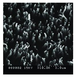
Field emission from carbon nanotubes (CNTs) was first reported in 1995 [1],[2]. With advancement in synthesis techniques, application of CNTs in field emission devices, such as field emission displays, gas discharge tubes and X-ray tube sources has been successfully demonstrated [3], [4]. Field emission performance of a single isolated CNT is found to be remarkable due to its structural integrity, geometry, chemical stability and high thermal conductivity. One can use a single CNT to produce an electron beam in a single electron beam device. However, in many applications (such as X-ray imaging systems), a continuous or patterned film is required to produce several independent electron beams. However, the situation in these cases becomes complex due to coupling among (i) the ballistic electron- phonon transport at moderate to high temperature range, (ii) field emission from each of the CNT tip and (iii) electrodynamic forces causing mechanical srain and deforming CNTs (and thus changing the electron density and dynamic conductivity). In such cases, the individual CNTs are not always inclined normal to the substrate surface (as shown in Fig. 1, where CNT tips are oriented in a random manner). This is the most common situation, which can evolve from an initially ordered state of uniformly distributed and vertically oriented CNTs. Such evolution process must be analyzed accurately from the view point of long-term performance of the device. The interest of the authors’ towards such an analysis and design studies stem from the problem of precision biomedical X-ray generation.
In this paper, we focus on a diode configuration, where the cathode contains a CNT thin film grown on a metallic substrate and the anode is a copper plate acting as emission current collector. Here, the most important requirement is to have a stable field emission current without compromising the lifetime of the device. As the CNTs in the film deplete with time, which is due to burning and fragmentation that result in a decreasing number of emitting sites, one observes fluctuation in the output current. Small spikes in the current have also been observed experimentally [5], which can generally be attributed to the change in the gap between the elongated CNT tip and the anode, and also possibly a dynamic contact of pulled up tip with the anode under high voltage. As evident from the reported studies [5], it is important to include various coupled phenomena in a numerical model, which can then be employed to understand the effects of various material parameters and also geometric parameters (e.g. CNT geometry as well as thin film patterns) on the collective field emission performance of the thin film device. Another aspect of interest in this paper is the effect of the angle of orientation of the CNT tips on the collective performance. A physics based modeling approach has been developed here to analyze the device-level performance of a CNT thin film.
2 MODEL FORMULATION
The physics of field emission from metallic surfaces is fairly well understood. The current density () due to field emission from a metallic surface is usually obtained by using the Fowler-Nordheim (FN) equation [6]
| (1) |
where E is the electric field, is the work function of the cathode material, and B and C are constants. However, in the case of a CNT thin film acting as cathode, the surface of the cathode is not smooth (like the metal emitters) and consists of hollow tubes in curved shapes and with certain spacings. An added complexity is the realignment of individual CNTs due to electrodynamic interaction between the neighbouring CNTs during field emission. Analysis of these processes requires the determination of the current density by considering the individual geometry of the CNTs, their dynamic orientations and the variation in the electric field during electronic transport.
Based on our previously developed model [7], which describes the degradation of CNTs and the CNT geometry and orientation, the rate of degradation of CNTs is defined as
| (2) |
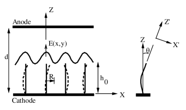
where is the representative volume element, is the concentration of carbon atoms in the cluster form in the cell, , , are lattice constants, and are integers . The pair defines the chirality of the CNT. Therefore, at a given time, the length of a CNT can be expressed as , where is the initial average height of the CNTs and is the distance between the cathode substrate and the anode (see Fig. 2).
The effective electric field component for field emission calculation in Eq. (1) is expressed as
| (3) |
where is the positive electronic charge and is the electrostatic potential energy. The total electrostatic potential energy can be expressed as
| (4) |
where is the constant source potential (on the substrate side), is the drain potential (on the anode side), is the Green’s function [8] with being the ring position, denotes the electron density at node position on the ring, and () denotes the chirality parameter of the CNT. The field emission current () from the anode surface associated with the elemental volume of the film is obtained as
| (5) |
where is the anode surface area and is the number of CNTs in the volume element. The toal current is obtained by summing the cell-wise current (). This formulation takes into account the effect of CNT tip orientations, and one can perform statistical analysis of the device current for randomly distributed and randomly oriented CNTs. However, due to the deformation of the CNTs due to electrodynamic forces, the evolution process requires a much more detailed treatment from the mechanics point of view.
Based on the studies reported in published literature, it is reasonable to expect that a major contribution is by the Lorentz force due to the flow of electron gas along the CNT and the ponderomotive force due to electrons in the oscillatory electric field . The oscillatory electric field could be due to hopping of the electrons along the CNT surfaces and the changing relative distances between two CNT surfaces. In addition, the electrostatic force and the van der Waals force are also important. The net force components acting on the CNTs parallel to the and the directions are calculated as [9]
| (6) |
| (7) |
where , , and are Lorentz, van der Waals, coulomb and ponderomotive forces, respectively and is the length of a small segment of CNTs. Next, we employ these force components in the expression of work done on the ensemble of CNTs and formulate an energy conservation law. Due to their large aspect ratio, the CNTs have been idealized as one-dimensional elastic members (as in Euler-Bernoulli beam). By introducing the strain energy density, the kinetic energy density and the work density, and applying the Hamilton principle, we obtain the governing equations in (, ) for each CNT, which can be expressed as
| (8) |
| (9) |
where and are lateral and longitudinal dispacements of the oriented CNTs, is the effective modulus of elasticity of CNTs, is the effective cross-sectional area, is the second moment of cross-sectional area about -axis, is the difference between the absolute temperature () during field emission and a reference temperature (), is the effective coefficient of thermal expansion (longitudinal), is the van der Waals coefficient, superscript indicates the th wall of the MWNT with as its radius, is the lateral displacement due to pressure and is the mass per unit length of CNT. We assume fixed boundary conditions () at the substrate-CNT interface () and forced boundary conditions at the CNT tip ().
The governing equation in temperature is obtained by the thermodynamics of electron-phonon interaction. By considering the Fourier heat conduction and thermal radiation from the surface of CNT, the energy rate balance equation in can be expressed as
| (10) |
where is the heat flux due to Joule heating over a segment of a CNT, is the Fourier heat conduction, is the diameter of the CNT and is the Stefan-Boltzmann constant. Here, we assume the emissivity to be unity. At the substrate-CNT interface (), the boundary condition is applied and at the tip we assign a reported estimate of the power dissipated by phonons exiting the CNT tip [10] to the conductive flux. We first compute the electric field at the nodes and then solve all the governing equations simultaneously at each time step and the curved shape of each of the CNTs is updated. The angle of orientation between the nodes and at the two ends of segment is expressed as
| (11) |
| (12) |
where is the usual coordinate transformation matrix which maps the displacements defined in the local coordinate system into the displacements defined in the cell coordinate system . For this transformation, we employ the angle obtained at the previous time step and for each node .
3 RESULTS AND DISCUSSIONS
The CNT film considered in this study consists of randomly oriented multiwalled CNTs. The film was grown on a stainless steel substrate. The film surface area (projected on anode) is 49.93 and the average thickness of the film (based on randomly distributed CNTs) is 10-14 . In the simulation and analysis, the constants B and C in Eq. (1) were taken as and , respectively [11]. It has been reported in the literature (e.g., [11]) that the work function for CNTs is smaller than the work functions for metal, silicon, and graphite. However, there are significant variations in the experimental values of depending on the types of CNTs (i.e., SWNT/MWNT), geometric parameters. The type of substrate materials have also significant influence on the electronic band-edge potential. The results reported in this paper are based on computation with .
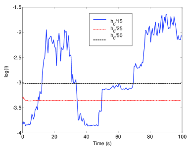
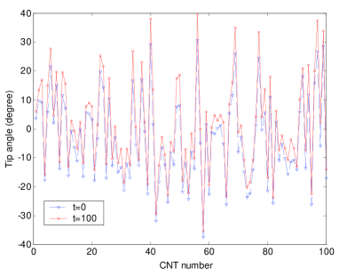
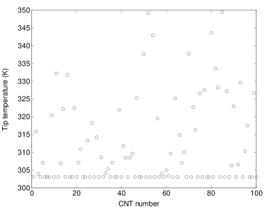
Following sample configuration has been used in this study: average height of CNTs , uniform diameter and uniform spacing between neighboring CNTs at the substrate contact region in the film . The initial height distribution and the orientation angle are randomly distributed. The electrode gap () is maintained at . The orientation of CNTs is parametrized in terms of the upper bound of the CNT tip deflection (denoted by , ). Several computational runs are performed and the output data are averaged out at each sampling time step. For a constant bias voltage ( in this case), as the initial state of deflection of the CNTs increases (from to ), the average current reduces until the initial state of deflection becomes large enough that the electrodynamic interaction among CNTs produces sudden pull in the deflected tips towards the anode resulting in current spikes (see Fig. 3). As mentioned earlier, spikes in the current have also been observed experimentally. Fig. 4 reveals that after experiencing the electrodynamic pull and Coulombic repulsion, some CNTs reorient themselves. In Fig. 5, maximum tip temperature distribution over an array of 100 CNTs during field emission over 100 s duration is plotted. The maximum temperature rises up to approximately 350 K.
4 CONCLUSION
In this paper, a model has been developed from the device design point of view, which sheds light on the coupling issues related to the mechanics, the thermodynamics, and the process of collective field emission from CNTs in a thin film, rather than a single isolated CNT. The proposed modeling approach handles several complexities at the device scale. While the previous works by the authors mainly dealt with decay, kinematics and dynamics of CNTs during field emission, this work includes some more aspects that were assumed constant earlier. These include: (i) non-local nature of the electric field, (ii) non-linear relationship between the electronic transport and the electric field, and (iii) non-linear relationship between the electronic transport and the heat conduction. The trend in the simulated results matches qualitatively well with the results of published experimental studies.
References
- [1] A.G. Rinzler, J.H. Hafner, P. Nikolaev, L. Lou, S.G. Kim, D. Tomanek, D. Colbert and R.E. Smalley, Science 269, 1550, 1995.
- [2] W.A. de Heer, A. Chatelain, and D. Ugrate, Science 270, 1179, 1995.
- [3] J.M. Bonard, J.P. Salvetat, T. Stockli, L. Forro and A. Chatelain, Appl. Phys. A 69, 245, 1999.
- [4] Y. Saito and S. Uemura, Carbon 38, 169, 2000.
- [5] J.M. Bonard, J.P. Salvetat, T. Stockli, L. Forro and A. Chatelain, Phys. Rev. B 67, 115406, 2003.
- [6] R.H. Fowler and L. Nordheim, Proc. Royal Soc. London A 119, 173, 1928.
- [7] N. Sinha, D. Roy Mahapatra, J.T.W. Yeow, R. Melnik and D. A. Jaffray, Proc. IEEE Nano 2006.
- [8] A. Svizhenko, M.P. Anantram and T.R. Govindan, IEEE Trans. Nanotech. 4, 557, 2005.
- [9] N. Sinha, D. Roy Mahapatra, J.T.W. Yeow, R. Melnik and D. A. Jaffray, J. comp. Theor. Nanosci. (Accepted).
- [10] H.-Y. Chiu, V.V. Deshpande, H.W.Ch. Postma, C.N. Lau, C. Mikó, L. Forró and M. Bockrath, Phys. Rev. Lett. 95, 226101, 2005.
- [11] Z.P. Huang, Y. Tu, D.L. Carnahan and Z.F. Ren, “Field emission of carbon nanotubes,” Encyclopedia of Nanoscience and Nanotechnology (Ed. H.S. Nalwa) 3, 401-416, 2004.