Carbon Nanotube Thin Film Field Emitting Diode:
Understanding the System Response Based on Multiphysics Modeling
N. Sinhaa, D. Roy Mahapatrab,
J.T.W. Yeowa111Corresponding author:
JTWY e-mail: jyeow@engmail.uwaterloo.ca;
Tel: 1 (519) 8884567 x 2152;
Fax: 1 (519) 7464791, R.V.N. Melnikb and
D.A. Jaffrayc
aDepartment of Systems Design Engineering,
University of Waterloo, ON, N2L3G1, Canada
bMathematical Modeling and Computational Sciences,
Wilfrid Laurier University, Waterloo,
ON, N2L3C5, Canada
cDepartment of Radiation Physics, Princess Margaret Hospital,
Toronto, ON, M5G2M9, Canada
Abstract
In this paper, we model the evolution and self-assembly of randomly oriented carbon nanotubes (CNTs), grown on a metallic substrate in the form of a thin film for field emission under diode configuration. Despite high output, the current in such a thin film device often decays drastically. The present paper is focused on understanding this problem. A systematic, multiphysics based modelling approach is proposed. First, a nucleation coupled model for degradation of the CNT thin film is derived, where the CNTs are assumed to decay by fragmentation and formation of clusters. The random orientation of the CNTs and the electromechanical interaction are then modeled to explain the self-assembly. The degraded state of the CNTs and the electromechanical force are employed to update the orientation of the CNTs. Field emission current at the device scale is finally obtained by using the Fowler-Nordheim equation and integration over the computational cell surfaces on the anode side. The simulated results are in close agreement with the experimental results. Based on the developed model, numerical simulations aimed at understanding the effects of various geometric parameters and their statistical features on the device current history are reported.
Keywords: Field emission, carbon nanotube, degradation, electrodynamics, self-assembly.
1 Introduction
The conventional mechanism used for electron emission is thermionic in nature where electrons are emitted from hot cathodes (usually heated filaments). The advantage of these hot cathodes is that they work even in environments that contain a large number of gaseous molecules. However, thermionic cathodes in general have slow response time and they consume high power. These cathodes have limited lifetime due to mechanical wear. In addition, the thermionic electrons have random spatial distribution. As a result, fine focusing of electron beam is very difficult. This adversely affects the performance of the devices such as X-ray tubes. An alternative mechanism to extract electrons is field emission, in which electrons near the Fermi level tunnel through the energy barrier and escape to the vacuum under the influence of a sufficiently high external electric field. The field emission cathodes have faster response time, consume less power and have longer life compared to thermionic cathodes. However, field emission cathodes require ultra-high vacuum as they are highly reactive to gaseous molecules during the field emission.
The key to the high performance of a field emission device is the behavior of its cathode. In the past, the performance of cathode materials such as spindt-type emitters and nanostructured diamonds for field emission was studied by Spindt et al.1 , Gotoh et al.2 , and Zhu3 . However, the spindt type emitters suffer from high manufacturing cost and limited lifetime. Their failure is often caused by ion bombardment from the residual gas species that blunt the emitter cones2 . On the other hand, nanostructured diamonds are unstable at high current densities3 . Carbon nanotube (CNT), which is an allotrope of carbon, has potential to be used as cathode material in field emission devices. Since their discovery by Iijima in 19914 , extensive research on CNTs has been conducted. Field emission from CNTs was first reported in 1995 by Rinzler et al.5 , de Heer et al.6 , and Chernozatonskii et al.7 . Field emission from CNTs has been studied extensively since then. Currently, with significant improvement in processing technique, CNTs are among the best field emitters. Their applications in field emission devices, such as field emission displays, gas discharge tubes, nanolithography systems, electron microscopes, lamps, and X-ray tube sources have been successfully demonstrated8-9 . The need for highly controlled application of CNTs in X-ray devices is one of the main reasons for the present study. The remarkable field emission properties of CNTs are attributed to their geometry, high thermal conductivity, and chemical stability. Studies have reported that CNT sources have a high reduced brightness and their energy spread values are comparable to conventional field emitters and thermionic emitters10 .
The physics of field emission from metallic surfaces is well understood. The current density () due to field emission from a metallic surface is usually obtained by using the Fowler-Nordheim (FN) equation11
| (1) |
where E is the electric field, is the work function of the cathode material, and B and C are constants. The device under consideration in this paper is a X-ray source where a thin film of CNTs acts as the electron emitting surface (cathode). Under the influence of sufficiently high voltage at ultra high vacuum, the electrons are extracted from the CNTs and hit the heavy metal target (anode) to produce X-rays. However, in the case of a CNT thin film acting as cathode, the surface of the cathode is not smooth (like the metal emitters). In this case, the cathode consists of hollow tubes grown on a substrate. Also, some amount of carbon clusters may be present within the CNT-based film. An added complexity is that there is realignment of individual CNTs due to electrodynamic interaction between the neighbouring CNTs during field emission. At present, there is no adequate mathematical models to address these issues. Therefore, the development of an appropriate mathematical modeling approach is necessary to understand the behavior of CNT thin film field emitters.
1.1 Role of various physical processes in the degradation of CNT field emitter
Several studies have reported experimental observations in favour of considerable degradation and failure of CNT cathodes. These studies can be divided into two categories: (i) studies related to degradation of single nanotube emitters12-17 and (ii) studies related to degradation of CNT thin films18-23 . Dean et al.13 found gradual decrease of field emission of single walled carbon nanotubes (SWNTs) due to “evaporation” when large field emitted current ( to ) was extracted. It was observed by Lim et al.23 that CNTs are susceptible to damage by exposure to gases such as oxygen and nitrogen during field emission. Wei et al.14 observed that after field emission over minutes at field emission current between and , the length of CNTs reduced by . Wang et al.15 observed two types of structural damage as the voltage was increased: a piece-by-piece and segment-by-segment splitting of the nanotubes, and a layer-by-layer stripping process. Occasional spikes in the current-voltage curves were observed by Chung et al.16 when the voltage was increased. Avouris et al.17 found that the CNTs break down when subjected to high bias over a long period of time. Usually, the breakdown process involves stepwise increases in the resistance. In the experiments performed by the present authors, peeling of the film from the substrate was observed at high bias. Some of the physics pertinent to these effects is known but the overall phenomenon governing such a complex system is difficult to explain and quantify and it requires further investigation.
There are several causes of CNT failures:
-
(i)
In case of multi-walled carbon nanotubes (MWNTs), the CNTs undergo layer-by-layer stripping during field emission15 . The complete removal of the shells are most likely the reason for the variation in the current voltage curves16 ;
-
(ii)
At high emitted currents, CNTs are resistively heated. Thermal effect can sublime a CNT causing cathode-initiated vacuum breakdown24 . Also, in case of thin films grown using chemical vapor deposition (CVD), fewer catalytic metals such as nickel, cobalt, and iron are observed as impurities in CNT thin films. These metal particles melt and evaporate by high emission currents, and abruptly surge the emission current. This results in vacuum breakdown followed by the failure of the CNT film23 ;
-
(iii)
Gas exposure induces chemisorption and physisorption of gas molecules on the surface of CNTs. In the low-voltage regime, the gas adsorbates remain on the surface of the emitters. On the other hand, in the high-voltage regime, large emission currents resistively anneal the tips, and the strong electric field on the locally heated tips promotes the desorption of gas adsorbates from the tip surface. Adsorption of materials with high electronegativity hinders the electron emission by intensifying the local potential barriers. Surface morphology can be changed by an erosion of the cap of the CNT as the gases desorb reactively from the surface of the CNTs25 ;
-
(iv)
CVD-grown CNTs tend to show more defects in the wall as their radius increases. Possibly, there are rearrangements of atomic structures (for example, vacancy migration) resulting in the reduction of length of CNTs14 . In addition, the presence of defects may act as a centre for nucleation for voltage-induced oxidation, resulting in electrical breakdown16 ;
-
(v)
As the CNTs grow perpendicular to the substrate, the contact area of CNTs with the substrate is very small. This is a weak point in CNT films grown on planar substrates, and CNTs may fail due to tension under the applied fields20 . Small nanotube diameters and lengths are an advantage from the stability point of view.
Although the degradation and failure of single nanotube emitters can be either abrupt or gradual, the degradation and failure of a thin film emitter with CNT cluster is mostly gradual. The gradual degradation occurs either during initial current-voltage measurement21 (at a fast time scale) or during measurements at constant applied voltage over a long period of time22 (at a slow time scale). Nevertheless, it can be concluded that the gradual degradation of thin films occurs due to the failure of individual emitters.
Till date, several studies have reported experimental observations on CNT thin films26 . However, from mathematical, computational and design view points, the models and characterization methods are available only for vertically aligned CNTs grown on the patterned surface27-28 . In a CNT film, the array of CNTs may ideally be aligned vertically. However, in this case it is desired that the individual CNTs be evenly separated in such a way that their spacing is greater than their height to minimize the screening effect29 . If the screening effect is minimized following the above argument, then the emission properties as well as the lifetime of the cathodes are adversely affected due to the significant reduction in density of CNTs. For the cathodes with randomly oriented CNTs, the field emission current is produced by two types of sources: (i) small fraction of CNTs that point toward the anode and (ii) oriented and curved CNTs subjected to electromechanical forces causing reorientation. As often inferred (see e.g., ref.29 ), the advantage of the cathodes with randomly oriented CNTs is that always a large number of CNTs take part in the field emission, which is unlikely in the case of cathodes with uniformly aligned CNTs. Such a thin film of randomly oriented CNTs will be considered in the present study. From the modeling point of view, its analysis becomes much more challenging. Although some preliminary works have been reported (see e.g., refs.30-31 ), neither a detailed model nor a subsequent characterization method are available that would allow to describe the array of CNTs that may undergo complex dynamics during the process of charge transport. In the detailed model, the effects of degradation and fragmentation of CNTs during field emission need to be considered. However, in the majority of analytical and design studies, the usual practice is to employ the classical Fowler-Nordheim equation11 to determine the field emission from the metallic surface, with correction factors to deal with the CNT tip geometry. Ideally, one has to tune such an empirical approach to specific materials and methods used (e.g. CNT geometry, method of preparation, CNT density, diode configuration, range of applied voltage, etc.). Also, in order to account for the oriented CNTs and interaction between themselves, it is necessary to consider the space charge and the electromechanical forces. By taking into account the evolution of the CNTs, a modeling approach is developed in this paper. In order to determine phenomenologically the concentration of carbon clusters due to degradation of CNTs, we introduce a homogeneous nucleation rate. This rate is coupled to a moment model for the evolution. The moment model is incorporated in a spatially discrete sense, that is by introducing volume elements or cells to physically represent the CNT thin film. Electromechanical forces acting on the CNTs are estimated in time-incremental manner. The oriented state of CNTs are updated using a mechanics based model. Finally, the current density is calculated by using the details regarding the CNT orientation angle and the effective electric field in the Fowler-Nordheim equation.
The remainder of this paper is organized as follows: in Sec. 2, a model is proposed, which combines the nucleation coupled model for CNT degradation with the electromechanical forcing model. Section 3 illustrates the computational scheme. Numerical simulations and the comparison of the simulated current-voltage characteristics with experimental results are presented in Sec. 4.
2 Model formulation
The CNT thin film is idealized in our mathematical model by using the following simplifications.
-
(i)
CNTs are grown on a substrate to form a thin film. They are treated as aggregate while deriving the nucleation coupled model for degradation phenomenologically;
-
(ii)
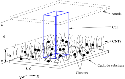
The film is discretized into a number of representative volume element (cell), in which a number of CNTs can be in oriented forms along with an estimated amount of carbon clusters. This is schematically shown in Fig. 1. The carbon clusters are assumed to be in the form of carbon chains and networks (monomers and polymers);
-
(iii)
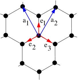
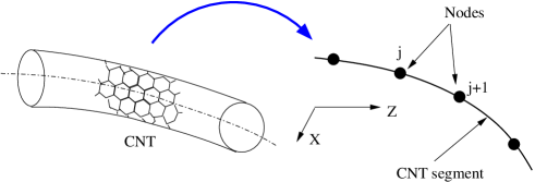
Each of the CNTs with hexagonal arrangement of carbon atoms (shown in Fig. 2(a)) are treated as effectively one-dimensional (1D) elastic members and discretized by nodes and segments along its axis as shown in Fig. 2(b). Deformation of this 1D representation in the slow time scale defines the orientations of the segments within the cell. A deformation in the fast time scale (due to electron flow) defines the fluctuation of the sheet of carbon atoms in the CNTs and hence the resulting state of atomic arrangements. The latter aspect is excluded from the present modeling and numerical simulations, however they will be discussed within a quantum-hydrodynamic framework in a forthcoming article.
2.1 Nucleation coupled model for degradation of CNTs
Let be the total number of carbon atoms (in CNTs and in cluster form) in a cell (see Fig. 1). The volume of a cell is given by , where is the cell surface interfacing the anode and is distance between the inner surfaces of cathode substrate and the anode. Let be the number of CNTs in the cell, and be the total number of carbon atoms present in the CNTs. We assume that during field emission some CNTs are decomposed and form clusters. Such degradation and fragmentation of CNTs can be treated as the reverse process of CVD or a similar growth process used for producing the CNTs on a substrate. Hence,
| (2) |
where is the total number of carbon atoms in the clusters in a cell at time and is given by
| (3) |
where is the concentration of carbon cluster in the cell. By combining Eqs. (2) and (3), one has
| (4) |
The number of carbon atom in a CNT is proportional to its length. Let the length of a CNT be a function of time, denoted as . Therefore, one can write
| (5) |
where is the number of carbon atoms per unit length of a CNT and can be determined from the geometry of the hexagonal arrangement of carbon atoms in the CNT. By combining Eqs. (4) and (5), one can write
| (6) |
In order to determine phenomenologically, we need to know the nature of evolution of the aggregate in the cell. From the physical point of view, one may expect the rate of formation of the carbon clusters from CNTs to be a function of thermodynamic quantities, such as temperature (), the relative distances () between the carbon atoms in the CNTs, the relative distances between the clusters and a set of parameters () describing the critical cluster geometry. The relative distance between carbon atoms in CNTs is a function of the electromechanical forces. Modeling of this effect is discussed in Sec. 2.2. On the other hand, the relative distances between the clusters influence in homogenizing the thermodynamic energy, that is, the decreasing distances between the clusters (hence increasing densities of clusters) slow down the rate of degradation and fragmentation of CNTs and lead to a saturation in the concentration of clusters in a cell. Thus, one can write
| (7) |
To proceed further, we introduce a nucleation coupled model32-33 , which was originally proposed to simulate aerosol formation. Here we modify this model according to the present problem which is opposite to the process of growth of CNTs from the gaseous phase. With this model the relative distance function is replaced by a collision frequency function () describing the frequency of collision between the -mers and -mers, with
| (8) |
and the set of parameters describing the critical cluster geometry by
| (9) |
where is the -mer volume, is the surface area of -mer, is the normalized critical cluster size, is the critical cluster diameter, is the Boltzmann constant, is the temperature and is the particle mass density. The detailed form of Eq. (7) is given by four nonlinear ordinary differential equations:
| (10) |
| (11) |
| (12) |
| (13) |
where is the kinetic normalization constant, is the kinetic nucleation rate, is the saturation ratio, is the total surface area of the carbon cluster and is the moment of cluster size distribution. The quantities involved are expressed as
| (14) |
| (15) |
| (16) |
where is the equilibrium saturation concentration of carbon cluster, is the maximum diameter of the clusters, is the cluster size distribution function, is the cluster diameter, is the mass of -mer, is the dimensionless surface tension given by
| (17) |
is the surface tension. In this paper, we have considered and for numerical simulations, that is, only monomer type clusters are considered. In Eqs. (10)-(13), the variables are , , and , and all other quantities are assumed constant over time. In the expression for moment in Eq. (14), the cluster size distribution in the cell is assumed to be Gaussian, however, random distribution can be incorporated. We solve Eqs. (10)-(13) using a finite difference scheme as discussed in Sec. 3. Finally, the number of CNTs in the cell at a given time is obtained with the help of Eq. (6), where the reduced length is determined using geometric properties of the individual CNTs as formulated next.
2.2 Effect of CNT geometry and orientation
It has been discussed in Sec. 1.1 that the geometry and orientation of the tip of the CNTs are important factors in the overall field emission performance of the film and must be considered in the model.
As an initial condition, let at , and let be the average height of the CNT region as shown in Fig. 1. This average height is approximately equal to the height of the CNTs that are aligned vertically. If is the decrease in the length of a CNT (aligned vertically or oriented as a segment) over a time interval due to degradation and fragmentation, and if is the diameter of the CNT, then the surface area of the CNT decreased is . By using the geometry of the CNT, the decreased surface area can be expressed as
| (18) |
where is the volume of the cell as introduced in Sec. 2.1, , , are the lattice constants, and (see Fig. 2(a)). The chiral vector for the CNT is expressed as
| (19) |
where and are integers and the pair defines the chirality of the CNT. The following properties hold: , , and . With the help of these properties the circumference and the diameter of the CNT can be expressed as, respectively34 ,
| (20) |
Let us now introduce the rate of degradation of the CNT or simply the burning rate as . By dividing both side of Eq. (18) by and by applying limit, one has
| (21) |
By combining Eqs. (20) and (21), the burning rate is finally obtained as
| (22) |
In Fig. 3 we show a schematic drawing of the CNTs almost vertically aligned, that is along the direction of the electric field . This electric field is assumed to be due to the applied bias voltage. However, there will be an additional but small amount of electric field due to several localized phenomena (e.g., electron flow in curved CNTs, field emission from the CNT tip etc.). Effectively, we assume that the distribution of the field parallel to -axis is of periodic nature (as shown in Fig. 3) when the CNT tips are vertically oriented. Only a cross-sectional view in the plane is shown in Fig. 3 because only an array of CNTs across -direction will be considered in the model for simplicity. Thus, in this paper, we shall restrict our attention to a two-dimensional problem, and out-of-plane motion of the CNTs will not be incorporated in the model.
To determine the effective electric field at the tip of a CNT oriented at an angle as shown in Fig. 3, we need to know the tip coordinate with respect to the cell coordinate system. If it is assumed that a CNT tip was almost vertically aligned at (as it is the desired configuration for the ideal field emission cathode), then its present height is and the present distance between the tip and the anode is . We assume that the tip electric field has a -dependence of the form , where and is the applied bias voltage. Also, let () be the deflection of the tip with respect to its original location and the spacing between the two neighboring CNTs at the cathode substrate is . Then the electric field at the deflected tip can be approximated as
| (23) |
where is a critical angle to be set during numerical calculations along with the condition: when . This is consistent with the fact that those CNTs which are low lying on the substrate do not contribute to the field emission. The electric field at the individual CNT tip derived here is defined in the local coordinate system () as shown in Fig. 3. The components of the electric field in the cell coordinate system () is given by the following transformation:
| (24) |
where , , are the direction cosines. According to the cell coordinate system in Figs. 1 and 3, , , and . Therefore, Eq. (24) can be rewritten as
| (25) |
By simplifying Eq. (25), we get
| (26) |
Note that the identical steps of this transformation also apply to a generally oriented () segment of CNT as idealized in Fig. 2(b). The electric field components and are later used for calculation of the electromechanical force acting on the CNTs. Since in this study we aim at estimating the current density at the anode due to the field emission from the CNT tips, we also use from Eq. (26) to compute the output current based on the Fowler-Nordheim equation (1).
2.3 Electromechanical forces
For each CNT, the angle of orientation is dependent on the electromechanical forces. Such dependence is geometrically nonlinear and it is not practical to solve the problem exactly, especially in the present situation where a large number of CNTs are to be dealt with. However, it is possible to solve the problem in time-dependent manner with an incremental update scheme. In this section we derive the components of the electromechanical forces acting on a generally oriented CNT segment. The numerical solution scheme based on an incremental update scheme will be discussed in Sec. 3.
From the studies reported in published literature and based on the discussions made in Sec. 1.1, it is reasonable to expect that the major contribution is due to (i) the Lorentz force under electron gas flow in CNTs (a hydrodynamic formalism), (ii) the electrostatic force (background charge in the cell), (iii) the van der Waals force against bending and shearing of MWNT and (iv) the ponderomotive force acting on the CNTs.
2.3.1 Lorentz force
It is known that the electrical conduction and related properties of CNTs depend on the mechanical deformation and the geometry of the CNT. In this paper we model the field emission behaviour of the CNT thin film by considering the time-dependent electromechanical effects, whereas the electronic properties and related effects are incorporated through the Fowler-Nordheim equation empirically. Electronic band-structure calculations are computationally prohibitive at this stage and at the same spatio-temporal scales considered for this study. However, a quantum-hydrodynamic formalism seems practical and such details will be dealt in a forthcoming article. Within the quantum-hydrodynamic formalism, one generally assumes the flow of electron gas along the cylindrical sheet of CNTs. The associated electron density distribution is related to the energy states along the length of the CNTs including the tip region. What is important for the present modeling is that the CNTs experience Lorentz force under the influence of the bias electric field as the electrons flow from the cathode substrate to the tip of a CNT. The Lorentz force is expressed as
| (27) |
where is the electronic charge, is the surface electron density corresponding to the Fermi level energy, is the electron density due to the deformation in the slow time scale, and phonon and electromagnetic wave coupling at the fast time scale, and is the electric field. The surface electron density corresponding to the Fermi level energy is expressed as35
| (28) |
where is the interatomic distance and is the overlap integral ( for carbon). The quantity can be related to the mechanical deformation of the 1D segments (See Fig. 2) and formulations reported by Xiao et al.36 can be employed. For simplicity, the electron density fluctuation is neglected in this paper. Now, with the electric field components derived in Eq. 26, the components of the Lorentz force acting along and directions can now be written as, respectively,
| (29) |
2.3.2 Electrostatic force
In order to calculate the electrostatic force, the interaction among two neighboring CNTs is considered. For such calculation, let us consider a segment on a CNT (denoted 1) and another segment on its neighboring CNT (denoted 2). These are parts of the representative 1D member idealized as shown in Fig. 2(b). The charges associated with these two segments can be expressed as
| (30) |
where and are diameters of two neighbouring CNTs (1) and (2). The electrostatic force on the segment by the segment is
where is the effective permittivity of the aggregate of CNTs and carbon clusters, is the permittivity of free space, and is the effective distance between the centroids of and . The electrostatic force on the segment due to charge in the entire segment () of the neighboring CNT (see Fig. 4) can be written as
The electrostatic force per unit length on due to is then
| (31) |
The differential of the force acts along the line joining the centroids of the segments and as shown in Fig. 4. Therefore, the components of the total electrostatic force per unit length of CNT (1) in and directions can be written as, respectively,
| (32) |
| (33) |
where is the angle the force vector makes with the -axis. For numerical computation of the above integrals, we compute the angle and at each of the centroids of the segments between the nodes and , where the length of the segments are assumed to be uniform and denoted as for CNT (1) and for CNT (2). As shown in Fig. 4, the distance between the centroids of the segments and is obtained as
| (34) |
where is the spacing between the CNTs at the cathode substrate, and are the deflections along -axis, and and are the deflections along -axis. The angle of projection is expressed as
| (35) |
The deflections , , , and are defined as, respectively,
| (36) |
| (37) |
| (38) |
| (39) |
Note that the total electrostatic force on a particular CNT is to be obtained by summing up all the binary contributions within the cell, that is by summing up Eqs. (32) and (33) over the upper integer number of the quantity , where is the number of CNTs in the cell as discussed in Sec. 2.1.
2.3.3 The van der Waals force
Next, we consider the van der Waals effect. The van der Waals force plays important role not only in the interaction of the CNTs with the substrate, but also in the interaction between the walls of MWNTs and CNT bundles. Due to the overall effect of forces and flexibility of the CNTs (here assumed to be elastic 1D members), the cylindrical symmetry of CNTs is destroyed, leading to their axial and radial deformations. The change in cylindrical symmetry may significantly affect the the properties of CNTs37-38 . Here we estimate the van der Waals forces due to the interaction between two concentric walls of the MWCNTs.
Let us assume that the lateral and the longitudinal displacements of a CNT be and , respectively. We use updated Lagrangian approach with local coordinate system for this description (similar to () system shown in Fig. 3), where the longitudinal axis coincides with and the lateral axis coincides with . Such a description is consistent with the incremental procedure to update the CNT orientations in the cells as adopted in the computational scheme. Also, due to the large length-to-diameter ratio (), let the kinematics of the CNTs, which are idealized in this work as 1D elastic members, be governed by that of an Euler-Bernoulli beam. Therefore, the kinematics can be written as
| (40) |
where the superscript indicates the th wall of the MWNT with as its radius and is the longitudinal displacement of the center of the cylindrical cross-section. Under tension, bending moment and lateral shear force, the elongation of one wall relative to its neighboring wall is
| (41) |
where we assume as the lateral displacement as some function of tensile force or compression buckling or pressure in the thin film device. The lateral shear stress () due to the van der Waals effect can now be written as
| (42) |
where is the van der Waals coefficient. Hence, the shear force per unit length can be obtained by integrating Eq. (42) over the individual wall circumferences and then by summing up for all the neighboring pair interactions, that is,
| (43) |
The components of van der Waals force in the cell coordinate system () is then obtained as
| (44) |
2.3.4 Ponderomotive force
Ponderomotive force, which acts on free charges on the surface of CNTs, tends to straighten the bent CNTs under the influence of electric field in the -direction. Furthermore, the ponderomotive forces induced by the applied electric field stretch every CNT39 . We add this effect by assuming that the free charge at the tip region is subjected to Ponderomotive force, which is computed as40
| (45) |
where is the surface area of the cell on the anode side, is the component of the Ponderomotive force and the component is assumed to be negligible.
2.4 Modelling the reorientation of CNTs
The net force components acting on the CNTs along and directions can be expressed as, respectively,
| (46) |
| (47) |
For numerical computation, at each time step the force components obtained using Eqs. (46) and (47) are employed to update the curved shape , where the displacements are approximated using simple beam mechanics solution:
| (48) |
| (49) |
where is the effective cross-sectional area, is the area moment, is the modulus of elasticity for the CNT under consideration. The angle of orientation, , of the corresponding segment of the CNT, that is between the node and node , is given by
| (50) |
| (51) |
where is the usual coordinate transformation matrix which maps the displacements () defined in the local () coordinate system into the displacements () defined in the cell coordinate system (). For this transformation, we employ the angle obtained in the previous time step and for each node .
3 Computational scheme
As already highlighted in the previous section, we model the CNTs as generally oriented 1D elastic members. These 1D members are represented by nodes and segments. With given initial distribution of the CNTs in the cell, we discretize the time into uniform steps . The computational scheme involves three parts: (i) discretization of the nucleation coupled model for degradation of CNTs derived in Sec. 2.1, (ii) incremental update of the CNT geometry using the estimated electromechanical force and (iii) computation of the field emission current in the device.
3.1 Discretization of the nucleation coupled model for degradation
With the help of Eqs. (14)-(16) and by eliminating the kinetic nucleation rate , we first rewrite the simplified form of Eqs. (10)-(13), which are given by, respectively,
| (52) |
| (53) |
| (54) |
| (55) |
By eliminating from Eq. (52) with the help of Eq. (53) and by applying a finite difference formula in time, we get
| (56) |
Similarly, Eqs. (53)-(55) are discretized as, respectively,
| (57) |
| (58) |
| (59) |
By simplifying Eq. (56) with the help of Eqs. (57)-(59), we get a quadratic polynomial of the form
| (60) |
where
| (61) |
| (62) |
| (63) |
Solution of Eq. (60) yields two roots (denoted by superscripts ):
| (64) |
For the first time step, the values of , and are obtained by applying the initial conditions: , , and . Since the must be real and finite, the following two conditions are imposed: and . Also, it has been assumed that the degradation of CNTs is an irreversible process, that is, the reformation of CNTs from the carbon cluster does not take place. Therefore, an additional condition of positivity, that is, is introduced while performing the time stepping. Along with the above constraints, the history in a cell is calculated as follows:
-
•
If and , then ;
-
•
Else if , then ;
-
•
Otherwise the value of remains the same as in the previous time step, that is, .
Simplification of Eq. (57) results in the following equation:
| (65) |
where
| (66) |
| (67) |
Solution of Eq. (65) yields the following two roots:
| (68) |
For the first time step, and are calculated with the following conditions: from the above calculation, , and . Realistically, the saturation ratio cannot be negative or equal to one. Therefore, yields .
While solving for , the Eq. (59) is solved with the values of and from the above calculations and the initial conditions , . The value of was calculated by assuming as a standard normal distribution function.
3.2 Incremental update of the CNT geometry
At each time time step , once the is solved, we are in a position to compute the net electromechanical force (see Sec. 2.3) as
| (69) |
Subsequently, the orientation angle for each segment of each CNT is then obtained as (see Sec. 2.4)
| (70) |
and it is stored for future calculations. A critical angle, (), is generally employed with to for the present numerical simulations. For , the meaning of is the “longitudinal force” and the meaning of is the “lateral force” in the context of Eqs. (48) and (49). When , the meanings of and are interchanged.
3.3 Computation of field emission current
Once the updated tip angles and the electric field at the tip are obtained at a particular time step, we employ Eq. (1) to compute the current density contribution from each CNT tip, which can be rewritten as
| (71) |
with and taken from ref.41 . The device current () from each computational cell with surface area at the anode at the present time step is obtained by summing up the current density over the number of CNTs in the cell, that is,
| (72) |
Fig. 5 shows the flow chart of the computational scheme discussed above.
At , in our model, the CNTs can be randomly oriented. This random distribution is parameterized in terms of the upper bound of the CNT tip deflection, which is given by , where is the CNT length and is a real number. In the numerical simulations which will be discussed next, the initial tip deflections can vary widely. The following values of the upper bound of the tip deflection have been considered: , . The tip deflection is randomized between zero and these upper bounds. Simulation for each initial input with a randomized distribution of tip deflections was run for a number of times and the maximum, minimum, and average values of the output current were obtained. In the first set, the simulations were run for a uniform height, radius and spacing of CNTs in the film. Subsequently, the height, the radius and the spacing were varied randomly within certain bounds, and their effects on the output current were analyzed.
4 Results and discussions
The CNT film under study in this work consists of randomly oriented multi-walled nanotubes (MWNTs). The film samples were grown on a stainless steel substrate. The film has a surface area of and thickness of . The anode consists of a thick copper plate with an area of . The current-voltage history is measured over a range of DC bias voltages for a controlled gap between the cathode and the anode. In the experimental set-up, the device is placed within a vacuum chamber of a multi-stage pump. The gap () between the cathode substrate and the anode is controlled from outside by a micrometer.
4.1 Degradation of the CNT thin films
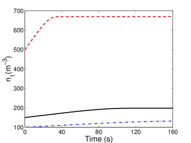
We assume that at , the film contains negligible amount of carbon cluster. To understand the phenomena of degradation and fragmentation of the CNTs, following three sets of input are considered: . The other initial conditions are set as , , , and . Fig. 6 shows the three histories over a small time duration () for the three cases of , respectively. For and , the time histories indicate that the rate of decay is very slow, which in turn implies longer lifetime of the device. For , the time history indicates that the CNTs decay comparatively faster, but still insignificant for the first , and then the cluster concentration becomes constant. It can be concluded from the above three cases that the rate of decay of CNTs is generally slow under operating conditions, which implies stable performance and longer lifetime of the device if this aspect is considered alone.
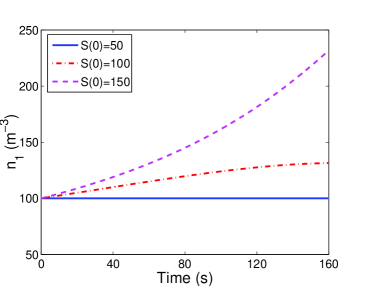
Next, the effect of variation in the initial saturation ratio on history is studied. The value of is set as , while other parameters are assumed to have identical value as considered previously. The following three initial conditions in are considered: . Fig. 7 shows the histories. It can be seen in this figure that for (moderate value), the carbon cluster concentration first increases and then tends to a steady state. This was also observed in Fig. (6). For higher values of , increases exponentially over time. For , a smaller value, the decay is not observed at all. This implies that a small value of is favorable for longer lifetime of the cathode. However, a more detailed investigation on the physical mechanism of cluster formation and CNT fragmentation may be necessary, which is an open area of research.
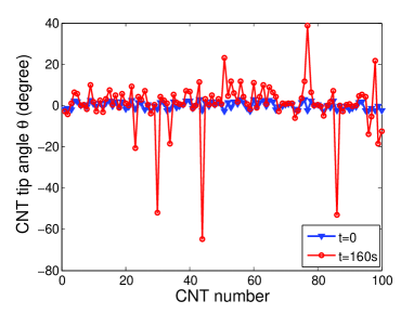
At , we assign random orientation angles () to the CNT segments. For a cell containing 100 CNTs, Fig. 8 shows the terminal distribution of the CNT tip angles (at corresponding to the case discussed previously) compared to the initial distribution (at ). The large fluctuations in the tip angles for many of the CNTs can be attributed to the significant electromechanical interactions.
4.2 Current-voltage characteristics
In the present study, the quantum-mechanical treatment has not been explicitly carried out, and instead, the Fowler-Nordheim equation has been used to calculate the current density. In such a semi-empirical calculation, the work function 42 for the CNTs must be known accurately under a range of conditions for which the device-level simulations are being carried out. For CNTs, the field emission electrons originate from several excited energy states (non metallic electronic states)43-44 . Therefore, the the work function for CNTs is usually not well identified and is more complicated to compute than for metals. Several methodologies for calculating the work function for CNTs have been proposed in literature. On the experimental side, Ultraviolet Photoelectron Spectroscopy (UPS) was used by Suzuki et al.45 to calculate the work function for SWNTs. They reported a work function value of 4.8 eV for SWNTs. By using UPS, Ago et al.46 measured the work function for MWNTs as 4.3 eV. Fransen et al.47 used the field emission electronic energy distribution (FEED) to investigate the work function for an individual MWNT that was mounted on a tungsten tip. Form their experiments, the work function was found to be eV. Photoelectron emission (PEE) was used by Shiraishi et al.48 to measure the work function for SWNTs and MWNTs. They measured the work function for SWNTs to be 5.05 eV and for MWNTs to be 4.95 eV. Experimental estimates of work function for CNTs were carried out also by Sinitsyn et al.49 . Two types were investigated by them: (i) 0.8-1.1 nm diameter SWNTs twisted into ropes of 10 nm diameter, and (ii) 10 nm diameter MWNTs twisted into 30-100 nm diameter ropes. The work functions for SWNTs and MWNTs were estimated to be 1.1 eV and 1.4 eV, respectively. Obraztsov et al.50 reported the work function for MWNTs grown by CVD to be in the range 0.2-1.0 eV. These work function values are much smaller than the work function values of metals (), silicon(), and graphite(). The calculated values of work function of CNTs by different techniques is summarized in Table 1. The wide range of work functions in different studies indicates that there are possibly other important effects (such as electromechanical interactions and strain) which also depend on the method of sample preparation and different experimental techniques used in those studies. In the present study, we have chosen .
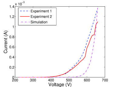
The simulated current-voltage (I-V) characteristics of a film sample for a gap is compared with the experimental measurement in Fig. 9. The average height, the average radius and the average spacing between neighboring CNTs in the film sample are taken as , , and . The simulated I-V curve in Fig. 9 corresponds to the average of the computed current for the ten runs. This is the first and preliminary simulation of its kind based on a multiphysics based modeling approach and the present model predicts the I-V characteristics which is in close agreement with the experimental measurement. However, the above comparison indicates that there are some deviations near the threshold voltage of , which needs to be looked at by improving the model as well as experimental materials and method.
4.3 Field emission current history
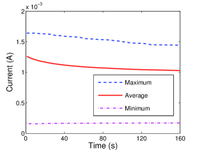
Next, we simulate the field emission current histories for the similar sample configuration as used previously, but for three different parametric variations: height, radius, and spacing. Current histories are shown for constant bias voltages of , and .
4.3.1 Effects of uniform height, uniform radius and uniform spacing
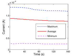
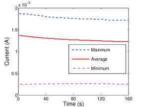
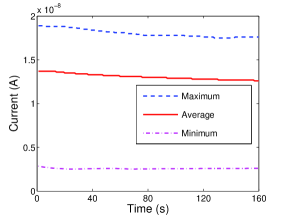
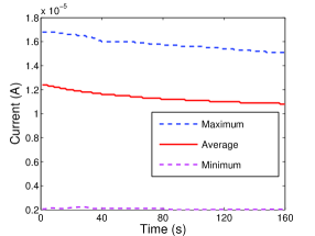
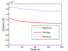
In this case, the values of height, radius, and the spacing between the neighboring CNTs are kept identical to the previous current-voltage calculation in Sec. 4.2. Fig. 10(a), (b) and (c) show the current histories for three different bias voltages of , and . In the subfigures, we plot the minimum, the maximum and the average currents over time as post-processed from a number of runs with randomized input distributions. At a bias voltage of , the average current decreases from to in steps. The maximum current varies between to , whereas the minimum current varies between to . Comparisons among the scales in the sub-figures indicate that there is an increase in the order of magnitude of current when the bias voltage is increased. The average current decreases from to in steps when the bias voltage is increased from to . At the bias voltage of , the average value of the current decreases from to . The increase in the order of magnitude in the current at higher bias voltage is due to the fact that the electrons are extracted with a larger force. However, at a higher bias voltage, the current is found to decay faster (see Fig. 10(c)).
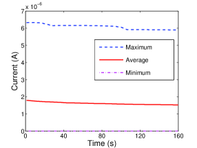
4.3.2 Effects of non-uniform radius
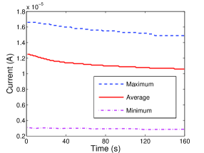
In this case, the uniform height and the uniform spacing between the neighboring CNTs are taken as and , respectively. Random distribution of radius is given with bounds . The simulated results are shown in Fig. 11. At the bias voltage of , the average current decreases from at to at in steps and then the current stabilizes. The maximum current varies between to , whereas the minimum current varies between to . The average current decreases from to in steps when the bias voltage is increased from to . At a bias voltage of , the average current decreases from to . As expected, a more fluctuation between the maximum and the minimum current have been observed here when compared to the case of uniform radius.
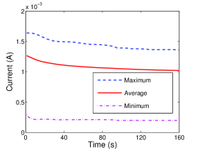
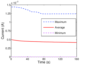
4.3.3 Effects of non-uniform height
In this case, the uniform radius and the uniform spacing between neighboring CNTs are taken as and , respectively. Random initial distribution of the height is given with bounds . The simulated results are shown in Fig. 12. At the bias voltage of , the average current decreases from to . The maximum current varies between to , whereas the minimum current varies between to . The average current decreases from to in steps when the bias voltage is increased from to . At the bias voltage of , the average current decreases from to . The device response is found to be highly sensitive to the height distribution.
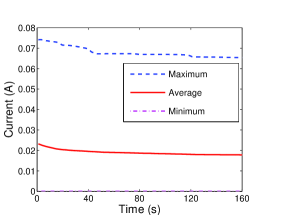
4.3.4 Effects of non-uniform spacing between neighboring CNTs
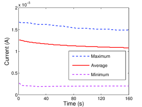
In this case, the uniform height and the uniform radius of the CNTs are taken as and , respectively. Random distribution of spacing between the neighboring CNTs is given with bounds . The simulated results are shown in Fig. 13. At the bias voltage of , the average current decreases from to . The maximum current varies between to , whereas the minimum current varies between to . The average current decreases from to in steps when the bias voltage is increased from to . At the bias voltage of , the average current decreases from to . There is a slight increase in the order of magnitude of current for non-uniform spacing. It can attributed to the reduction in screening effect at some emitting sites in the film where the spacing is large.
5 Conclusions
In this paper, we have developed a multiphysics based modelling approach to analyze the evolution of the CNT thin film. The developed approach has been applied to the simulation of the current-voltage characteristics at the device scale. First, a phenomenological model of degradation and fragmentation of the CNTs has been derived. From this model we obtain degraded state of CNTs in the film. This information, along with electromechanical force, is then employed to update the initially prescribed distribution of CNT geometries in a time incremental manner. Finally, the device current is computed at each time step by using the semi-empirical Fowler-Nordheim equation and integration over the computational cell surfaces on the anode side. The model thus handles several important effects at the device scale, such as fragmentation of the CNTs, formation of the carbon clusters, and self-assembly of the system of CNTs during field emission. The consequence of these effects on the I-V characteristics is found to be important as clearly seen from the simulated results which are in close agreement with experiments. Parametric studies reported in the concluding part of this paper indicate that the effects of the height of the CNTs and the spacing between the CNTs on the current history is significant at the fast time scale.
There are several other physical factors, such as the thermoelectric heating, interaction between the cathode substrate and the CNTs, time-dependent electronic properties of the CNTs and the clusters, ballistic transport etc., which may be important to consider while improving upon the model developed in the present paper. Effects of some of these factors have been discussed in the literature before in the context of isolated CNTs, but little is known at the system level. We note also that in the present model, the evolution mechanism is not fully coupled with the electromechanical forcing mechanism. The incorporation of the above factors and the full systematic coupling into the modelling framework developed here presents an appealing scope for future work.
Acknowledgment The authors would like to thank Natural Sciences and Engineering Research Council (NSERC), Canada, for financial support.
References
- [1] C. A. Spindt, I. Brodie, L. Humphrey and E. R. Westerberg, J. Appl. Phys. 47, 5248 (1976).
- [2] Y. Gotoh, M. Nagao, D. Nozaki, K. Utsumi, K. Inoue, T. Nakatani, T, Sakashita, K. Betsui, H. Tsuji and J. Ishikawa, J. Appl. Phys. 95, 1537 (2004).
- [3] W. Zhu (Ed.), Vacuum microelectronics, Wiley, NY (2001).
- [4] S. Iijima, Nature 354, 56 (1991).
- [5] A. G. Rinzler, J. H. Hafner, P. Nikolaev, L. Lou, S. G. Kim, D. Tomanek, D. Colbert and R. E. Smalley, Science 269, 1550 (1995).
- [6] W. A. de Heer, A. Chatelain and D. Ugrate, Science 270, 1179 (1995).
- [7] L. A. Chernozatonskii, Y. V. Gulyaev, Z. Y. Kosakovskaya, N. I. Sinitsyn, G. V. Torgashov, Y. F. Zakharchenko, E. A. Fedorov and V. P. Valchuk, Chem. Phys. Lett. 233, 63 (1995).
- [8] J. M. Bonard, J. P. Salvetat, T. Stockli, L. Forro and A. Chatelain, Appl. Phys. A 69, 245 (1999).
- [9] H. Sugie, M. Tanemure, V. Filip, K. Iwata, K. Takahashi and F. Okuyama, Appl. Phys. Lett. 78, 2578 (2001).
- [10] O. Groening, O. M. Kuettel, C. Emmenegger, P. Groening, and L. Schlapbach, J. Vac. Sci. Tech. B18, 665 (2000).
- [11] R. H. Fowler, and L. Nordheim, Proc. Royal Soc. London A 119, 173 (1928).
- [12] J. M. Bonard, F. Maier, T. Stockli, A. Chatelain, W. A. de Heer, J. P. Salvetat and L. Forro, Ultramicroscopy 73, 7 (1998).
- [13] K. A. Dean, T. P. Burgin and B. R. Chalamala, Appl. Phys. Lett. 79, 1873 (2001).
- [14] Y. Wei, C. Xie, K. A. Dean and B. F. Coll, Appl. Phys. Lett. 79, 4527 (2001).
- [15] Z. L. Wang, R. P. Gao, W. A. de Heer and P. Poncharal, Appl. Phys. Lett. 80, 856 (2002).
- [16] J. Chung, K. H. Lee, J. Lee, D. Troya, and G. C. Schatz, Nanotechnology 15, 1596 (2004).
- [17] P. Avouris, R. Martel, H. Ikeda, M. Hersam, H. R. Shea and A. Rochefort, in Fundamental Mater. Res. Series, M. F. Thorpe (Ed.), Kluwer Academic/Plenum Publishers (2000) pp.223-237.
- [18] L. Nilsson, O. Groening, P. Groening and L. Schlapbach, Appl. Phys. Lett. 79, 1036 (2001).
- [19] L. Nilsson, O. Groening, P. Groening and L. Schlapbach, J. Appl. Phys. 90, 768 (2001).
- [20] J. M. Bonard, C. Klinke, K. A. Dean and B. F. Coll, Phys. Rev. B 67, 115406 (2003).
- [21] J. M. Bonard, N. Weiss, H. Kind, T. Stockli, L. Forro, K. Kern and A. Chatelain, Adv. Matt. 13, 184 (2001).
- [22] J. M. Bonard, J. P. Salvetat, T. Stockli, W. A. de Heer, L. Forro and A. Chatelain, Appl. Phys. Lett. 73, 918 (1998).
- [23] S. C. Lim, H. J. Jeong, Y. S. Park, D. S. Bae, Y. C. Choi, Y. M. Shin, W. S. Kim, K. H. An and Y. H. Lee, J. Vac. Sci. Technol. A 19, 1786 (2001).
- [24] N. Y. Huang, J. C. She, J. Chen, S. Z. Deng, N. S. Xu, H. Bishop, S. E. Huq, L. Wang, D. Y. Zhong, E. G. Wang and D. M. Chen, Phys. Rev. Lett. 93, 075501 (2004).
- [25] X. Y. Zhu, S. M. Lee, Y. H. Lee and T. Frauenheim, Phys. Rev. Lett. 85, 2757 (2000).
- [26] P. G. Collins and A. Zettl, Appl. Phys. Lett. 69, 1969 (1996).
- [27] D. Nicolaescu, L. D. Filip, S. Kanemaru and J. Itoh, Jpn. J. Appl. Phys. 43, 485 (2004).
- [28] D. Nicolaescu, V. Filip, S. Kanemaru and J. Itoh, J. Vac. Sci. Technol. 21, 366 (2003).
- [29] Y. Cheng and O. Zhou, Electron field emission from carbon nanotubes, C. R. Physique 4, 1021 (2003).
- [30] N. Sinha, D. Roy Mahapatra, J. T. W. Yeow, R. V. N. Melnik and D. A. Jaffray, Proc. 6th IEEE Conf. Nanotech., Cincinnati, USA, July 16-20 (2006).
- [31] N. Sinha, D. Roy Mahapatra, J. T. W. Yeow, R. V. N. Melnik and D. A. Jaffray, Proc. 7th World Cong. Comp. Mech., Los Angeles, USA, July 16-22 (2006).
- [32] S. K. Friedlander, Ann. N.Y. Acad. Sci. 404, 354 (1983).
- [33] S. L. Grishick, C. P. Chiu and P. H. McMurry, Aerosol Sci. Technol. 13, 465 (1990).
- [34] H. Jiang, P. Zhang, B. Liu, Y. Huang, P. H. Geubelle, H. Gao and K. C. Hwang, Comp. Mat. Sci. 28, 429 (2003).
- [35] G. Y. Slepyan, S. A. Maksimenko, A. Lakhtakia, O. Yevtushenko and A. V. Gusakov, Phys. Rev. B 60, 17136 (1999).
- [36] J. R. Xiao B. A. Gama and J. W. Gillespie Jr., Int. J. Solids Struct. 42, 3075 (2005).
- [37] R. S. Ruoff, J. Tersoff, D. C. Lorents, S. Subramoney and B. Chan, Nature 364, 514 (1993).
- [38] T. Hertel, R. E. Walkup and P. Avouris, Phys. Rev. B 58, 13870 (1998).
- [39] O. E. Glukhova, A. I. Zhbanov, I. G. Torgashov, N. I. Sinistyn and G. V. Torgashov, Appl. Surf. Sci. 215, 149 (2003).
- [40] A. L. Musatov, N. A. Kiselev, D. N. Zakharov, E. F. Kukovitskii, A. I. Zhbanov, K. R. Izrael’yants and E. G. Chirkova, Appl. Surf. Sci. 183, 111 (2001).
- [41] Z. P. Huang, Y. Tu, D. L. Carnahan and Z. F. Ren, in Encycl. Nanosci. Nanotechnol. 3, Edited by H. S. Nalwa, American Scientific Publishers, Los Angeles (2004), pp.401-416.
- [42] J. W. Gadzuk and E. W. Plummer, Rev. Mod. Phys. 45, 487 (1973).
- [43] K. A. Dean, O. Groening, O. M. Kuttel and L. Schlapbach, Appl. Phys. Lett. 75, 2773 (1999).
- [44] A. Takakura, K. Hata, Y. Saito, K. Matsuda, T. Kona and C. Oshima, Ultramicroscopy 95, 139 (2003).
- [45] S. Suzuki, C. Bower, Y. Watanabe and O. Zhou, Appl. Phys. Lett. 76, 4007 (2000).
- [46] H. Ago, T. Kugler, F. Cacialli, W. R. Salaneck, M. S. P. Shaffer, A. H. Windle and R. H. Friend, J. Phys. Chem. B 103, 8116 (1999).
- [47] M. J. Fransen, T. L. van Rooy and P. Kruit, Appl. Surf. Sci. 146, 312 (1999).
- [48] M. Shiraishi and M. Ata, Carbon 39, 1913 (2001).
- [49] N. I. Sinitsyn, Y. V. Gulyaev, G. V. Torgashov, L. A. Chernozatonskii, Z. Y. Kosakovskaya, Y. F. Zakharchenko, N. A. Kiselev, A. L. Musatov, A. I. Zhbanov, S. T. Mevlyut and O. E. Glukhova, Appl. Surf. Sci. 111, 145 (1997).
- [50] A. N. Obraztsov, A. P. Volkov and I. Pavlovsky, Diam. Rel. Mater. 9, 1190 (2000).
| Type of CNT | () | Method |
|---|---|---|
| SWNT | 4.8 | Ultraviolet photoelectron spectroscopy45 |
| MWNT | 4.3 | Ultraviolet photoelectron spectroscopy46 |
| MWNT | 7.30.5 | Field emission electronic energy distribution47 |
| SWNT | 5.05 | Photoelectron emission48 |
| MWNT | 4.95 | Photoelectron emission48 |
| SWNT | 1.1 | Experiments49 |
| MWNT | 1.4 | Experiments49 |
| MWNT | 0.2-1.0 | Numerical approximation50 |
(a) (b)


(a) (b) (c)
(a) (b) (c)
(a) (b) (c)
(a) (b) (c)