Reversed flow at low frequencies in a microfabricated AC electrokinetic pump
Abstract
Microfluidic chips have been fabricated to study electrokinetic pumping generated by a low voltage AC signal applied to an asymmetric electrode array. A measurement procedure has been established and followed carefully resulting in a high degree of reproducibility of the measurements. Depending on the ionic concentration as well as the amplitude of the applied voltage, the observed direction of the DC flow component is either forward or reverse. The impedance spectrum has been thoroughly measured and analyzed in terms of an equivalent circuit diagram. Our observations agree qualitatively, but not quantitatively, with theoretical models published in the literature.
I Introduction
The recent interest in AC electrokinetic micropumps was initiated by experimental observations by Green, Gonzales et al. of fluid motion induced by AC electroosmosis over pairs of microelectrodes Green2000 ; Gonzales2000 ; Green2002 and by a theoretical prediction by Ajdari that the same mechanism would generate flow above an electrode array Ajdari2000 . Brown et al. Brown2000 demonstrated experimentally pumping of electrolyte with a low voltage, AC biased electrode array, and soon after the same effect was reported by a number of other groups observing flow velocities of the order of mm/s Studer2002 ; Mpholo2003 ; Lastochkin2004 ; Debesset2004 ; Studer2004 ; Cahill2004 ; Ramos2005 ; Garcia2006 . Several theoretical models have been proposed parallel to the experimental observations Ramos2003 ; Mortensen2005 ; LHO2006 . However, so far not all aspects of the flow-generating mechanisms have been explained.
Studer et al. Studer2004 made a thorough investigation of flow dependence on electrolyte concentration, driving voltage and frequency for a characteristic system. In this work a reversal of the pumping direction for frequencies above 10 kHz and rms voltages above 2 V was reported. For a travelling wave device Ramos et al. Ramos2005 observed reversal of the pumping direction at 1 kHz and voltages above 2 V. The reason for this reversal is not yet fully understood and the goal of this work is to contribute with further experimental observations of reversing flow for other parameters than those reported previously.
An integrated electrokinetic AC driven micropump has been fabricated and studied. The design follows Studer et al. Studer2004 , where an asymmetric array of electrodes covers the channel bottom in one section of a closed pumping loop. Pumping velocities are measured in another section of the channel without electrodes. In this way electrophoretic interaction between the beads used as flow markers and the electrodes is avoided. In contrast to the soft lithography utilized by Studer et al., we use more well-defined MEMS fabrication techniques in Pyrex glass. This results in a very robust system, which exhibits stable properties and remains functional over time periods extending up to a year. Furthermore, we have a larger electrode coverage of the total channel length allowing for the detection of smaller pumping velocities. Our improved design has led to the observation of a new phenomenon, namely the reversing of the flow at low voltages and low frequencies. The electrical properties of the fabricated microfluidic chip have been investigated to clarify whether these reflect the reversal of the flow direction. In accordance with the electrical measurements we propose and evaluate an equivalent circuit diagram. Supplementary details related to the present work can be found in Ref. MIGthesis .
II Experimental
II.1 System design
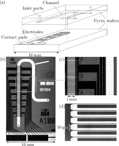
The microchip was fabricated for studies of the basic electrokinetic properties of the system. Hence, a simple microfluidic circuit was designed to eliminate potential side-effects due to complex device issues. The chip consists of two 500 m thick Pyrex glass wafers anodically bonded together. Metal electrodes are defined on the bottom wafer and channels are contained in the top wafer, as illustrated schematically in Fig. 1(a). This construction ensures an electrical insulated chip with fully transparent channels.
An electrode geometry akin to the one utilized by Brown et al. Brown2000 and Studer et al. Studer2004 was chosen. The translation period of the electrode array is 50 m with electrode widths of m and m, and corresponding electrode spacings of m and m, see Fig. 1(d). Further theoretical investigations have shown that this geometry results in a nearly optimal flow velocity LHO2006 . The total electrode array consists of eight sub-arrays each having their own connection to the shared contact pad, Fig. 1(b). This construction makes it possible to disconnect a malfunctioning sub-array. The entire electrode array has a width of 1.3 mm ensuring that the alignment of the electrodes and the 1.0 mm wide fluidic channels is not critical.
A narrow side channel, Fig. 1(b), allows beads to be introduced into the part of the channel without electrodes, where a number of ruler lines with a spacing of 200 m enable flow measurements by particle tracing, Fig. 1(c).
An outer circuit of valves and tubes is utilized to control and direct electrolytes and bead solutions through the channels. During flow-velocity measurements, the inlet to the narrow side channel is blocked and to eliminate hydrostatic pressure differences the two ends of the main channel are connected by an outer teflon tube with an inner diameter of 0.5 mm. The hydraulic resistance of this outer part of the pump loop is three orders of magnitude smaller than the on-chip channel resistance and is thus negligible.
The maximal velocity of the Poiseuille flow in the measurement channel section is denoted , and the average slip velocity generated above the electrodes by electroosmosis is denoted . To obtain a measurable at as low applied voltages as possible, the electrode coverage of the total channel length is made as large as possible. In our system the total channel length is and the section containing electrodes is , which ensures a high Poiseuille flow velocity, MIGthesis .
The microfluidic chip has a size of approximately and is shown in Fig. 1, and the device parameters are listed in Table 1.
| Channel height | ||
|---|---|---|
| Channel width | ||
| Channel length | ||
| Channel length with electrodes | ||
| Width of electrode array | ||
| Narrow electrode gap | ||
| Wide electrode gap | ||
| Narrow electrode width | ||
| Wide electrode width | ||
| Electrode thickness | ||
| Electrode surface area () | ||
| Electrode surface area () | ||
| Number of electrode pairs | ||
| Electrode resistivity (Pt) | ||
| Electrolyte conductivity (0.1 mM) | ||
| Electrolyte conductivity (1.0 mM) | ||
| Electrolyte permittivity | ||
| Pyrex permittivity |
II.2 Chip fabrication
The flow-generating electrodes of e-beam evaporated Ti(10 nm)/Pt(400 nm) were defined by lift-off in 1.5 m thick photoresist AZ 5214-E (Hoechst) using a negative process. The Ti layer ensures good adhesion to the Pyrex substrate. Platinum is electrochemically stable and has a low resistivity, which makes it suitable for the application. By choosing an electrode thickness of nm, the metallic resistance between the contact pads and the channel electrolyte is at least one order of magnitude smaller than the resistance of the bulk electrolyte covering the electrode array.
In the top Pyrex wafer the channel of width m and height m was etched into the surface using a solution of 40% hydrofluoric acid. A 100 nm thick amorphous silicon layer was sputtered onto the wafer surface and used as etch mask in combination with a 2.2 m thick photoresist layer. The channel pattern was defined by a photolithography process akin to the process used for electrode definition, and the wafer backside and edges were protected with a 70 m thick etch resistant PVC foil. The silicon layer was then etched away in the channel pattern using a mixture of nitric acid and buffered hydrofluoric acid, HNO3:BHF:H2O = 20:1:20. The wafer was subsequently baked at 120∘C to harden the photoresist prior to the HF etching of the channels. Since the glass etching is isotropic, the channel edges were left with a rounded shape. However, this has only a minor impact on the flow profile, given that the channel aspect ratio is . The finished wafer was first cleaned in acetone, which removes both the photoresist and the PVC foil, and then in a piranha solution.
After alignment of the channel and the electrode array, the two chip layers were anodically bonded together by heating the ensemble to 400∘C and applying a voltage difference of 700 V across the two wafers for 10 min. During this bonding process, the previously deposited amorphous Si layer served as diffusion barrier against the sodium ions in the Pyrex glass. Finally, immersing the chip in DI-water holes were drilled for the in- and outlet ports using a cylindrical diamond drill with a diameter of 0.8 mm.
II.3 Measurement setup and procedures
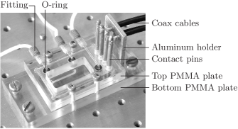
Liquid injection and electrical contact to the microchip was established through a specially constructed PMMA chip holder, shown in Fig. 2. Teflon tubing was fitted into the holder in which drilled channels provided a connection to the on-chip channel inlets. The interface from the chip holder to the chip inlets was sealed by O-rings. Electrical contact was obtained with spring loaded contact pins fastened in the chip holder and pressed against the electrode pads. The inner wires of thin coax cables were soldered onto the pins and likewise fastened to the holder.
The pumping was induced by electrolytic solutions of KCl in concentrations ranging from mM to 1.0 mM. The chip was prepared for an experiment by careful injection of this electrolyte into the channel and tubing system, after which the three valves to in- and outlets were closed. The electrical impedance spectrum of the microchip was measured before and after each series of flow measurements to verify that no electrode damaging had occurred during the experiments. If the impedance spectrum had changed, the chip and the series of performed measurements were discarded. Velocity measurements were only carried out when the tracer beads were completely at rest before biasing the chip, and it was always verified that the beads stopped moving immediately after switching off the bias. The steady flow was measured for 10 s to 30 s. After a series of measurements was completed, the system was flushed thoroughly with milli-Q water. When stored in milli-Q water between experiments the chips remained functional for at least one year.
II.4 AC biasing and impedance measurements
Using an impedance analyzer (HP 4194 A), electrical impedance spectra of the microfluidic chip were obtained by four-point measurements, where each contact pad was probed with two contact pins. Data was acquired from 100 Hz to 15 MHz. To avoid electrode damaging by application of a too high voltage at low frequencies, all impedance spectra were measured at mV.
The internal sinusoidal output signal of a lock-in amplifier (Stanford Research SR830DSP) was used for AC biasing of the electrode array during flow-velocity measurements. The applied rms voltages were in the range from 0.5 V to 2 V and the frequencies between 0.5 kHz and 100 kHz. A current amplification was necessary to maintain the correct potential difference across the electrode array, since the overall chip resistance could be small ( to 1 k) when frequencies in the given interval were applied. The current through the microfluidic chip was measured by feeding the output signal across a small series resistor back into the lock-in amplifier.
The lock-in amplifier was also used for measuring impedance spectra for frequencies below 100 Hz, which were beyond the span of the impedance analyzer.
II.5 Flow velocity measurements
After filling the channel with an electrolyte and actuating the electrodes, the flow measurements were performed by tracing beads suspended in the electrolyte.
Fluorescent beads (Molecular Probes, FluoSpheres F-8765) with a diameter of 1 m were introduced into the measurement section of the channel and used as flow markers for the velocity determination. A stereo microscope was focused at the beads, and with an attached camera pictures were acquired with time intervals of s to 1.00 s depending on the bead velocity. Subsequently, the velocity was determined by averaging over a distance of m, i.e., . Only the fastest beads were used for flow detection, since these are assumed to be located in the vertical center of the channel. It should be noted that the use of fluorescent particles prevented an introduction of significant illumination heating of the sample.
The limited number of acquired pictures led to an uncertainty of 5% in the determination of flow velocities, which corresponds to the movement of the tracer beads within to frame. Additionally, there is a statistical uncertainty on the vertical particle position in the channel, which is estimated to introduce up to 10% error on the determined bead velocity. It is then assumed that the fastest beads are positioned within of the maximum of the Poiseuille flow profile.
III Results
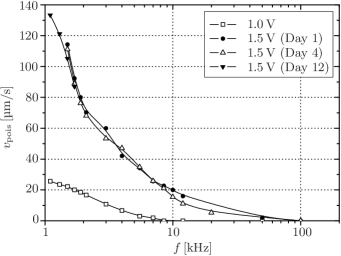
In the parameter ranges corresponding to those published in the literature, our flow velocity measurements are in agreement with previously reported results. Using a mM KCl solution and driving voltages of V to 1.5 V over a frequency range of kHz to 100 kHz, we observed among other measurement series the pumping velocities shown in Fig. 3. The general tendencies were an increase of velocity towards lower frequencies and higher voltages, and absence of flow above kHz. The measured velocities corresponded to slightly more than twice those measured by Studer et al. Studer2004 due to our larger electrode coverage of the total channel. We observed damaging of the electrodes if more than 1 V was applied to the chip at a driving frequency below 1 kHz, for which reason there are no measurements at these frequencies. It is, however, plausible that the flow velocity for our chip peaked just below kHz.
III.1 Reproducibility of measurements
Our measured flow velocities were very reproducible due to the employed MEMS chip fabrication techniques and the careful measurement procedures described in Sec. II. This is illustrated in Fig. 3, which shows three velocity series recorded several days apart. The measurements were performed on the same chip and for the same parameter values. Between each series of measurements, the chip was dismounted and other experiments performed. However, it should be noted that a very slow electrode degradation was observed when a dozen of measurement series were performed on the same chip over a couple of weeks.
III.2 Low frequency reversed flow
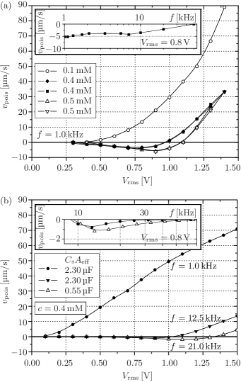
Devoting special attention to the low-frequency ( kHz), low-voltage regime ( V), not studied in detail previously, we observed an unanticipated flow reversal for certain parameter combinations. Fig. 4(a) shows flow velocities measured for a frequency of 1.0 kHz as a function of applied voltage for various electrolyte concentrations. It is clearly seen that the velocity series of mM exhibits the known exclusively forward and increasing pumping velocity as function of voltage, whereas for slightly increased electrolyte concentrations an unambiguous reversal of the flow direction is observed for rms voltages below approximately 1 V.
This reversed flow direction was observed for all frequencies in the investigated spectrum when the electrolyte concentration and the rms voltage were kept constant. This is shown in the inset of Fig. 4(a), where a velocity series was obtained over the frequency spectrum for an electrolyte concentration of 0.4 mM at a constant rms voltage of 0.8 V. It is noted that the velocity is nearly constant over the entire frequency range and tends to zero above kHz.
III.3 Electrical characterization
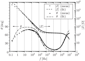
To investigate whether the flow reversal was connected to unusual properties of the electrical circuit, we carefully measured the impedance spectrum of the microfluidic system. Spectra were obtained for the chip containing KCl electrolytes with the different concentrations mM, 0.4 mM and 1.0 mM.
Fig. 5 shows the Bode plots of the impedance spectrum obtained for mM. For frequencies between Hz and Hz the curve shape of the impedance amplitude is linear with slope , after which a horizontal curve section follows, and finally the slope again becomes for frequencies above Hz. Correspondingly, the phase changes between and . From the decrease in phase towards low frequencies it is apparent that must have another horizontal curve section below Hz. When the curve is horizontal and the phase is the system behaves resistively, while it is capacitively dominated when the phase is and the curve has a slope of .
| Debye length | |
| Total electrode resistance | |
| Total bulk electrolyte resistance | |
| Total faradaic (charge transfer) resistance | |
| Internal resistance in lock-in amplifier | |
| Total measured resistance for | |
| Total electrode capacitance | |
| Total double layer capacitance | |
| Debye layer capacitance | |
| Surface capacitance | |
| Debye frequency | |
| Inverse ohmic relaxation time | |
| Inverse faradaic charge transfer time (primarily) | |
| Characteristic frequency of electrode circuit |
| [M rad s-1] | [k rad s-1] | ||||||||||||
|---|---|---|---|---|---|---|---|---|---|---|---|---|---|
III.4 Equivalent circuit
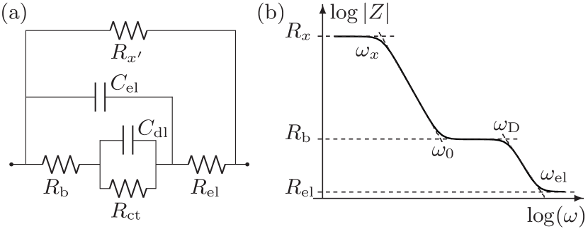
In electrochemistry the standard way of analyzing such impedance measurements is in terms of an equivalent circuit diagram BardFaulkner . The choice of diagram is not unambiguous Green2002 . We have chosen the diagram shown in Fig. 6(a) with the component labeling listed in Table 2.
Charge transport through the bulk electrolyte is represented by an ohmic resistance , accumulation of charge in the double layer at the electrodes by a capacitance , and faradaic current injection from electrochemical reactions at the electrodes by another resistance, the charge-transfer resistance BardFaulkner ; LHO2006 . Moreover, we include the ohmic resistance of the metal electrodes , the mutual capacitance between the narrow and wide electrodes , and a shunt resistance M to represent the internal resistance of the lock-in amplifier.
Finally, in electrochemical experiments at low frequency, the electrical current is often limited by diffusive transport of the reactants in the faradaic electrode reaction to and from the electrodes. This can be modeled by adding a frequency dependent Warburg impedance in series with the charge transfer resistance BardFaulkner . However, because the separation between the electrodes is so small and the charge transfer resistance is so large, we are unable to distinguish the Warburg impedance in the impedance measurements and leave it out of the equivalent diagram.
By fitting the circuit model to the impedance measurements we extract the component values listed in Table 3. On the chip labeled B we were unable to measure the charge transfer resistance due to a minor error on the chip introduced during the bonding process. Fig. 6(b) illustrates the relation between component values and the impedance amplitude curve through four characteristic angular frequencies . The inverse frequency primarily expresses the characteristic time for the faradaic charge transfer into the Debye layer. The characteristic time for charging the Debye layer through the electrolyte is given by . The Debye frequency is , and finally simply states the characteristic frequency for the on-chip electrode circuit in the absence of electrolyte. It is noted that the total DC-limit resistance corresponds to the parallel coupling between and .
IV Discussion
In the following we investigate to which extent the general theory of induced-charge (AC) electroosmosis can explain our observations and experimental data. We first use the equivalent circuit component values extracted from the impedance measurements to estimate some important electrokinetic parameters based on the Gouy–Chapman–Stern model BardFaulkner , namely, the Stern layer capacitance , the intrinsic zeta potential on the electrodes and the charge transfer resistance . Then we use this as input to the weakly nonlinear electro-hydrodynamic model presented in Ref. LHOthesis , which is an extension of the model in Ref. LHO2006 . We compare theoretical values with experimental observations, and discuss the experimentally observed trends of the flow velocities.
IV.1 Impedance analysis
The impedance measurements are performed at a low voltage of mV so it might be expected that Debye–Hückel linear theory applies ( mV). However, since we only measure the potential difference between the electrodes and we do not know the potential of the bulk electrolyte, we cannot say much about the exact potential drop across the double layer. Many electrode-electrolyte systems posses an intrinsic zeta potential at equilibrium of up to a few hundred mV. Indeed, the measured is roughly times larger than predicted by Debye–Hückel theory, which indicates that the intrinsic zeta potential is at least mV.
According to Gouy–Chapman–Stern theory the can be expressed as a series coupling of the compact Stern layer capacitance and the differential Debye-layer capacitance ,
| (1) |
where the two double-layer capacitances of an electrode pair are coupled in series through the electrolyte, and since the electrode pairs are coupled in parallel, the effective area of the total double layer is . and are the total surface areas exposed to the electrolyte of a narrow and wide electrode, respectively. For simplicity is often assumed constant and independent of potential and concentration, while is given by the Gouy–Chapman theory as
| (2) |
Unfortunately, it is not possible to estimate the exact values of both and from a measurement of , because a range of parameters lead to the same . We can, nevertheless, state lower limits as F/m2 and mV for mM or F/m2 and mV at mM.
For the model values in Table 3 we used Eq. (1) with F/m2 and mV, 160 mV and 140 mV at 0.1 mM, 0.4 mM and 1.0 mM KCl, respectively, in accordance with the trend often observed that decreases with increasing concentration, Kirby2004 . The bulk electrolyte resistance can be expressed as
| (3) |
where is the conductivity, is the width of the electrodes and is the number of electrode pairs, see Table 1, and is a numerical factor computed for our particular electrode layout using the finite-element based program Comsol Multiphysics. Similarly, the mutual capacitance between the electrodes can be calculated as
| (4) |
and the resistance of the electrodes leading from the contact pads to the array is simply estimated from the resistivity of platinum and the electrode geometry.
At frequencies above 100 kHz the impedance is dominated by , and , and the Bode plot closely resembles a circuit with ideal components, see Fig. 5. Around 1 kHz we observe some frequency dispersion which could be due to the change in electric field line pattern around the inverse RC-time LHOthesis . Finally, below 1 kHz where the impedance is dominated by , the phase never reaches indicating that the double layer capacitance does not behave as an ideal capacitor but more like a constant phase element (CPE). This behavior is well known experimentally, but not fully understood theoretically Kerner2000 .
IV.2 Flow
The forward flow velocities measured at mM as a function of frequency, Fig. 3, qualitatively exhibit the trends predicted by standard theory, namely, the pumping increases with voltage and falls off at high frequency Ajdari2000 ; Ramos2003 .
More specifically, the theory predicts that the pumping velocity should peak at a frequency around the inverse RC-time , corresponding to kHz, and decay as the inverse of the frequency for our applied driving voltages, see Fig. 11 in Ref. LHO2006 . Furthermore, the velocity is predicted to grow like the square of the driving voltage at low voltages, changing to at large voltages LHO2006 ; LHOthesis .
Experimentally, the velocity is indeed proportional to and the peak is not observed within the range 1.1 kHz to 100 kHz, but it is likely to be just below 1 kHz. However, the increase in velocity between 1.0 V and 1.5 V displayed in Fig. 3 is much faster than . That is also the result in Fig. 4(a) for mM where no flow is observed below V, while above that voltage the velocity increases rapidly. For mM and mM the velocity even becomes negative at voltages V. This cannot be explained by the standard theory and is also rather different from the reverse flow that has been observed by other groups at larger voltages V and at frequencies above the inverse RC-time Studer2004 ; Ramos2005 ; Garcia2006 .
The velocity shown in the inset of Fig. 4(a) is remarkable because it is almost constant between 1 kHz and 10 kHz. This is unlike the usual behavior for AC electroosmosis that always peaks around the inverse RC-time, because it depends on partial screening at the electrodes to simultaneously get charge and tangential field in the Debye layer. At lower frequency the screening is almost complete so there is no electric field in the electrolyte to drive the electroosmotic fluid motion, while at higher frequency the screening is negligible so there is no charge in the Debye layer and again no electroosmosis.
One possible explanation for the almost constant velocity as a function of frequency could be that the amount of charge in the Debye layer is controlled by a faradaic electrode reaction rather than by the ohmic current running through the bulk electrolyte. Our impedance measurement clearly shows that the electrode reaction is negligible at kHz and mV bias, but since the reaction rate grows exponentially with voltage in an Arrhenius type dependence, it may still play a role at V. However, previous theoretical investigations have shown that faradaic electrode reactions do not lead to reversal of the AC electroosmotic flow or pumping direction LHO2006 .
Due to the strong nonlinearity of the electrode reaction and the asymmetry of the electrode array, there may also be a DC faradaic current running although we drive the system with a harmonic AC voltage. In the presence of an intrinsic zeta potential on the electrodes and/or the glass substrate this would give rise to an ordinary DC electroosmotic flow. This process does not necessarily generate bubbles because the net reaction products from one electrode can diffuse rapidly across the narrow electrode gap to the opposite electrode and be consumed by the reverse reaction.
To investigate to which extent this proposition applies, we used the weakly nonlinear theoretical model presented in LHOthesis . The model extends the standard model for AC electroosmosis by using the Gouy–Chapman–Stern model to describe the double layer, and Butler–Volmer reaction kinetics to model a generic faradaic electrode reaction BardFaulkner . The concentration of the oxidized and reduced species in the diffusion layer near the electrodes is modeled by a generalization of the Warburg impedance, while the bulk concentration is assumed uniform, see Ref. LHOthesis for details.
The model parameters are chosen in accordance with the result of the impedance analysis, i.e., F/m2, M, mV, as discussed in Sec. IVA. Further we assume an intrinsic zeta potential of mV on the borosilicate glass walls Kirby2004 , and choose (arbitrarily) an equilibrium bulk concentration of 0.02 mM for both the oxidized and the reduced species in the electrode reaction, which is much less than the KCl electrolyte concentration of mM.
The result of the model calculation is shown in Fig. 4(b). At 1 kHz the fluid motion is dominated by AC electroosmosis which is solely in the forward direction. However, at 12.5 kHz the AC electroosmosis is much weaker and the model predicts a (small) reverse flow due to the DC electroosmosis for V.
Fig. 4(b) shows that the frequency interval with reverse flow is only from 30 kHz down to 10 kHz, while the measured velocities remain negative down to at least 1 kHz. The figure also shows results obtained with a lower Stern layer capacitance F/m2 in the model, which turns out to enhance the reverse flow.
In both cases, the reverse flow predicted by the theoretical model is weaker than that observed experimentally and does not show the almost constant reverse flow profile below 10 kHz. Moreover, the model is unable to account for the strong concentration dependence displayed in Fig. 4(a).
According to Ref. Bazant2006a , steric effects give rise to a significantly lowered Debye layer capacitance and a potentially stronger concentration dependence when exceeds mV, which roughly corresponds to a driving voltage of V. Thus, by disregarding these effects we overestimate the double layer capacitance slightly in the calculations of the theoretical flow velocity for V. This seems to fit with the observed tendencies, where theoretical velocity curves calculated on the basis of a lowered better resemble the measured curves.
Finally, it should be noted that several electrode reactions are possible for the present system. As an example we mention . This reaction is limited by the amount of oxygen present in the solution, which in our experiment is not controlled. If this reaction were dominating the faradaic charge transfer, the value of could change from one measurement series to another.
V Conclusion
We have produced an integrated AC electrokinetic micropump using MEMS fabrication techniques. The resulting systems are very robust and may preserve their functionality over years. Due to careful measurement procedures it has been possible over weeks to reproduce flow velocities within the inherent uncertainties of the velocity determination.
An hitherto unobserved reversal of the pumping direction has been measured in a regime, where the applied voltage is low ( V) and the frequency is low ( kHz) compared to earlier investigated parameter ranges. This reversal depends on the exact electrolytic concentration and the applied voltage. The measured velocities are of the order m/s to m/s. Previously reported studies of flow measured at the same parameter combinations show zero velocity in this regime Studer2004 . The reason why we are able to detect the flow reversal is probably our design with a large electrode coverage of the channel leading to a relative high ratio .
Finally, we have performed an impedance characterization of the pumping devices over eight frequency decades. By fitting Bode plots of the data, the measured impedance spectra compared favorably with our model using reasonable parameter values.
The trends of our flow velocity measurements are accounted for by a previously published theoretical model, but the quantitative agreement is lacking. Most important, the predicted velocities do not depend on electrolyte concentration, yet the concentration seems to be one of the causes of our measured flow reversal, Fig. 4(a). This shows that there is a need for further theoretical work on the electro-hydrodynamics of these systems and in particular on the effects of electrolyte concentration variation.
Acknowledgements.
We would like to thank Torben Jacobsen, Department of Chemistry (DTU), for enlightening discussions about electrokinetics and the interpretation of impedance measurements on electrokinetic systems.References
- (1) N. G. Green, A. Ramos, A. Gonzalez, H. Morgan and A. Castellanos, Phys. Rev. E 61(4), 4011 (2000).
- (2) A. Gonzalez, A. Ramos, N. G. Green, A. Castellanos and H. Morgan, Phys. Rev. E 61(4), 4019 (2000).
- (3) N. G. Green, A. Ramos, A. Gonzalez, H. Morgan and A. Castellanos, Phys. Rev. E 66, 026305 (2002).
- (4) A. Ajdari, Phys. Rev. E 61, R45 (2000).
- (5) A. B. D. Brown, C. G. Smith and A. R. Rennie, Phys. Rev. E 63, 016305 (2000).
- (6) V. Studer, A. Pépin, Y. Chen and A. Ajdari, Microelectron. Eng. 61-62, 915 (2002).
- (7) M. Mpholo, C. G. Smith and A. B. D. Brown, Sens. Actuators B 92, 262 (2003).
- (8) D. Lastochkin, R. Zhou, P. Whang, Y. Ben and H.-C. Chang, J. Appl. Phys. 96, 1730 (2004).
- (9) S. Debesset, C. J. Hayden, C. Dalton, J. C. T. Eijkel and A. Manz, Lab Chip 4, 396 (2004).
- (10) V. Studer, A. Pépin, Y. Chen and A. Ajdari, The Analyst 129, 944 (2004).
- (11) B. P. Cahill, L. J. Heyderman, J. Gobrecht and A. Stemmer, Phys. Rev. E 70, 036305 (2004).
- (12) A. Ramos, H. Morgan, N. G. Green, A. Gonzalez and A. Castellanos, J. Appl. Phys. 97, 084906 (2005).
- (13) P. García–Sánchez, A. Ramos, N. G. Green and H. Morgan, IEEE Trans. Dielect. El. In. 13, 670 (2006).
- (14) A. Ramos, A. Gonzalez, A. Castellanos, N. G. Green and H. Morgan, Phys. Rev. E 67, 056302 (2003).
- (15) N. A. Mortensen, L. H. Olesen, L. Belmon and H. Bruus, Phys. Rev. E 71, 056306 (2005).
- (16) L. H. Olesen, H. Bruus and A. Ajdari, Phys. Rev. E 73, 056313 (2006).
- (17) M. M. Gregersen, AC Asymmetric Electrode Micropumps, MSc Thesis, MIC - Dept. of Micro and Nanotechnology, DTU (2005), www.mic.dtu.dk/mifts
- (18) M. S. Kilic, M. Z. Bazant and A. Ajdari, Phys. Rev. E 75, 021502 (2007) and Phys. Rev. E 75, 021503 (2007).
- (19) L. H. Olesen, AC Electrokinetic micropumps, PhD Thesis, MIC - Dept. of Micro and Nanotechnology, DTU (2006), www.mic.dtu.dk/mifts
- (20) A. J. Bard and L. R. Faulkner, Electrochemical Methods, 2. ed. (Wiley, 2001).
- (21) B. J. Kirby and E. F. Hasselbrink, Electrophoresis 25, 187 (2004).
- (22) Z. Kerner and T. Pajkossy, Electrochim. Acta 46, 207 (2000).