Electrical transport properties of polar heterointerface between KTaO3 and SrTiO3
Abstract
Electrical transport of a polar heterointerface between two insulating perovskites, KTaO3 and SrTiO3, is studied. It is formed between a thin KTaO3 film deposited on a top of TiO2-terminated (100) SrTiO3 substrate. The resulting (KO)1-(TiO2)0 heterointerface is expected to be hole-doped according to formal valences of K (1+) and Ti (4+). We observed electrical conductivity and mobility in the KTaO3/SrTiO3 similar to values measured earlier in electron-doped LaAlO3/SrTiO3 heterointerfaces. However, the sign of the charge carriers in KTaO3/SrTiO3 obtained from the Hall measurements is negative. The result is an important clue to the true origin of the doping at perovskite oxide hetero-interfaces.
pacs:
73.20.-r,73.21.Ac,73.40.-cThe mechanism of doping in hetero-interfaces between two insulating perovskite oxides has been intensively discussed since the observation of large electrical conductivity in the hetero-structure between LaAlO3 (LAO) and SrTiO3 (STO). Ohtomo2004 ; Huijben2006 ; Thiel2006 ; Kalabukhov2007 ; Herranz2006 ; Siemons2006 It was argued that when a thin LAO film is coherently grown on the TiO2-terminated STO substrate, the resulting interface (LaO)+(TiO2)0 is expected to be polar, provided that the bulk formal valences of Ti and La are maintained at the interface and that the structure of the interface is atomically perfect. The polar structure at the interface results in an infinitely growing electrostatic potential in the (001) direction when the thickness of LAO film is increasing. In order to compensate for the charge discontinuity at the interface, half of an electron per square unit cell may be released leading to conductivity at the interface. Nakagawa2006 The possibility of this doping mechanism was supported by theoretical works. Pentcheva2006 ; Park2006 However, there are other possible doping mechanisms in perovskite oxides. It is well known that electrical properties of STO can be changed from insulating to metallic ones by a small reduction of oxygen from its stoichiometric composition. Tufte1967 ; Koonce1967 The possibility that the electrical property at the LAO/STO heterointerface is not due to the oxygen vacancies was presumably ruled out by keeping the STO substrate at deposition conditions which does not result in bulk conductivity due to oxygen vacancies. However, it is still possible that the deposition of the LAO film itself can reduce oxygen from a shallow layer at the STO substrate, as argued by Siemons et al. Siemons2006 We have previously suggested that oxygen vacancies play an important role in the electrical properties of the LAO/STO heterointerface. Kalabukhov2007 However, the true microscopic origin of the conductivity at the interface between LAO and STO could not be understood.
In this work we treat another polar interface between two insulating perovskite oxides, KTaO3 (KTO) and STO. KTO is a well known material with a cubic structure and lattice parameter of 3.99 Å(compare with 3.905 Åin STO). It is incipient ferroelectric at room temperature with a dielectric constant of about 260. Bozinis1976 ; Bae2004 Tantalum has a formal valence of 5+, and potassium 1+ in KTO. The KTO film should grow as a sequence of layers on a single TiO2-terminated STO substrate in the (001) direction and the resulting interface should have the structure of (KO)-(TiO2)0. This means that half a hole per square unit cell should be released. This is opposite to the (LaO)+(TiO2)0 heterointerface, where half an electron per unit cell is transferred to the interface.
We have grown thin KTO films on STO substrates and found that the KTO/STO interface is indeed conducting with electrical properties very similar to the LAO/STO interface. However, the charge of electrical carriers deduced from Hall effect measurements is negative. We discuss possible reasons for this interesting result in view of interface structure and possible doping mechanisms.
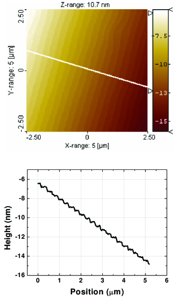
KTO films were prepared by pulsed laser deposition with in-situ reflection high-energy electron diffraction (RHEED) used to monitor film growth during deposition. The growth conditions were similar to what we used previously to fabricate LAO/STO hetero-interfaces: Kalabukhov2007 deposition temperature TD = 750 ∘C, oxygen pressure pO2 = mbar, laser energy density J = 1.5 J/cm2. RHEED oscillations could be observed during the initial part of the film growth. However the intensity decreased rapidly and after 3 unit cells it was too low to observe oscillations. The deposition rate estimated from the first RHEED oscillations was 1 unit cell per 10 pulses. The thickness of the KTO films was 13 u.c. layers (approx. 6 nm). Atomic force microscopy (AFM) showed very smooth step-like surface of the KTO film, see Fig.1.
Electrical measurements were made in a four point van der Pauw configuration Pauw1958 in the temperature range 2 K – 300 K and in magnetic field up to 5 T. First we proved that the KTO film itself is not conducting by using ”soft” contacts: silver wires glued on the film surface using silver epoxy. In order to reach the interface, we used Ti/Au contact pads fabricated by sputtering through metal mask. The resistance between Ti/Au contacts and contacts glued by silver epoxy was above 10 M, indicating an absence of pinholes in the KTO film.
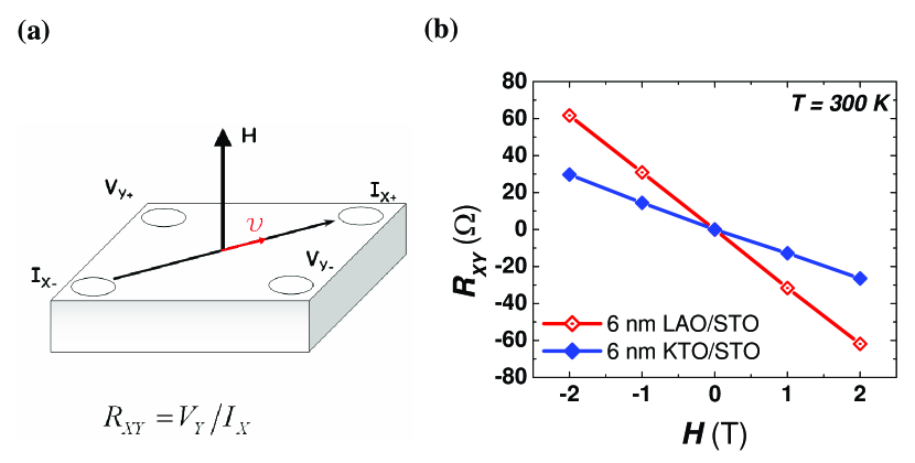
The electrical properties of KTO films may be compared to those of 15 u.c. thick LAO films on TiO2-terminated STO substrates prepared in the same conditions. Both hetero-structures show metallic conductivity with relatively high mobilities and charge carrier concentrations. Fig.2 shows Hall resistances measured at room temperature under the same experimental configuration (i.e. magnetic field and current direction, see Fig.2a). Both KTO/STO and LAO/STO heterointerfaces had the same sign of Hall coefficient. The sign of the charge carriers is negative according to the magnetic field and bias current directions.
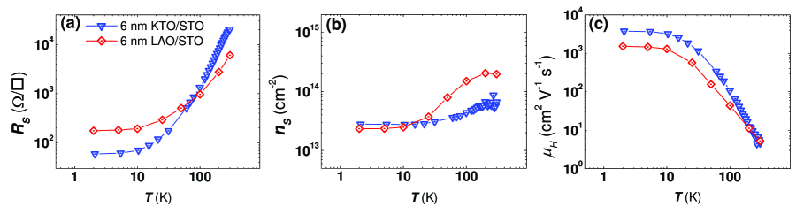
The values of the sheet resistance , the Hall mobility and the charge carrier density of the KTO/STO heterointerfaces are very similar to those of LAO/STO, see Fig.3. We measured three KTO films prepared in similar deposition conditions and they all showed similar transport properties.
It is known that potassium deficiency is a significant problem in growth of KTO films due to the high vapor pressure of potassium at high temperatures. Bae2004 If this were the case here, the actual heterointerface between KTO/STO may have different reconstruction from the one described above. This possibility needs to be ruled out in a future determination of the microstructure of the hetero-structure by electron microscopy.
Independent of the KTO/STO heterointerface microstructure being perfect or not, it is quite remarkable that the electrical properties are very similar to those of LAO/STO heterointerface. This could suggests that there is a common doping mechanism where the type and concentration of charge carriers do not directly depend on the sign of the polar interface deduced from the formal bulk valences. We have previously argued that the high conductivity, mobility, and charge carrier density found in hetero-junctions of LAO/STO prepared at low oxygen pressure mainly are due to oxygen vacancies residing in STO close to the interface. That conclusion is further strengthened by the present findings.
The work was supported by the Swedish KAW, SSF, and VR foundations, the EU NANOXIDE, and ESF THIOX programs.
References
- (1) A. Ohtomo, and H.Y. Hwang, Nature 427, 423 (2004); 441, 120 (2006).
- (2) M. Huijben, G. Rijnders,D. H. A. Blank, S. Bals, S. van Aert, J. Verbeeck, G. van Tendeloo, A. Brinkman and H. Hilgenkamp, Nature Materials 5, 556 (2006).
- (3) S. Thiel, G. Hammerl, A. Schmehl, C. W.Schneider and J. Mannhart, Science 313, 1935 (2006).
- (4) A. Kalabukhov, R. Gunnarsson, J. Börjesson, E. Olsson, T. Claeson and D. Winkler, Phys. Rev. B 75, 121404(R) (2007).
- (5) G. Herranz, M. Basletic, M. Bibes, R. Ranchal, A. Hamzic, E. Tafra, K. Bouzehouane, E. Jacquet, J. P. Contour, A. Barthelemy and A. Fert, Phys. Rev. B 73, 064403 (2006).
- (6) W. Siemons, G. Koster, H. Yamamoto, W. A. Harrison, G. Lukovsky, T. H. Geballe, D. H. A. Blank and M. R. Beasley, cond-mat/0612223 (2006).
- (7) N. Nakagawa, H. Y. Hwang and D. A. Muller, Nature Mat., 5, 204 (2006).
- (8) R. Pentcheva and W. E. Pickett, Phys. Rev. B 74, 035112 (2006)
- (9) M. S. Park, S. H. Rhim and A. J. Freeman, Phys. Rev. B 74, 205416 (2006)
- (10) O. N. Tufte and P. W. Chapman, Phys. Rev. 155, 796 (1967).
- (11) C. S. Koonce, M. L. Cohen, J. F. Schooley, W. R. Hosler and E. R. Pfeiffer, Phys. Rev. 163, 380 (1967).
- (12) D. Z. Bozinis, J. P. Hurrel, Phys. Rev. B 13, 3109 (1976).
- (13) H.-J. Bae, J. Sigman, S.-J. Park, Y.-H. Heo, L. A. Boatner and D. P. Norton, Solid State Electronics 48, 51 (2004).
- (14) J. L. van der Pauw Philips Res. Rep. 13, 1 (1958).
- (15)