Controlling surface statistical properties using bias voltage: Atomic force microscopy and stochastic analysis
Abstract
The effect of bias voltages on the statistical properties of rough surfaces has been studied using atomic force microscopy technique and its stochastic analysis. We have characterized the complexity of the height fluctuation of a rough surface by the stochastic parameters such as roughness exponent, level crossing, and drift and diffusion coefficients as a function of the applied bias voltage. It is shown that these statistical as well as microstructural parameters can also explain the macroscopic property of a surface. Furthermore, the tip convolution effect on the stochastic parameters has been examined.
pacs:
05.10.Gg, 02.50.Fz, 68.37.-dI Introduction
As device dimensions continue to shrink into the deep submicron size regime, there will be increasing attention for understanding the thin-film growth mechanism and the kinetics of growing rough surfaces in various deposition methods. To perform a quantitative study on surfaces roughness, analytical and numerical treatments of simple growth models propose, quite generally, the height fluctuations have a self-similar character and their average correlations exhibit a dynamic scaling form Barabasi ; Halpin ; Krug ; Meakin ; Kardar ; Masoudi . In these models, roughness of a surface is a smooth function of the sample size and growth time (or thickness) of films. In addition, other statistical quantities such as the average frequency of positive slope level crossing, the probability density function (PDF), as well as drift and diffusion coefficients provide further complete analysis on roughness of a surface. Very recently, it has been shown that, by using these statistical variables in the Langevin equation, regeneration of rough surfaces with the same statistical properties of a nanoscopic imaging is possible Jafari ; Waechter .
In practice, one of the effective ways to modify roughness of surfaces is applying a negative bias voltage during deposition of thin films Ohring , while their sample size and thickness are constant. In bias sputtering, electric fields near the substrate are modified to vary the flux and energy of incident charged species. This is achieved by applying either a negative DC or RF bias to the substrate. Due to charge exchange processes in the anode dark space, very few discharge ions strike the substrate with full bias voltage. Rather a broad low energy distribution of ions bombard the growing films.
Generally, bias sputtering modifies film properties such as surface morphology, resistivity, stress, density, adhesion, and so on through roughness improvement of the surface, elimination of interfacial voids and subsurface porosity, creation of a finer and more isotropic grain morphology, and the elimination of columnar grains Ohring .
In this work, the effect of bias voltage on the statistical properties of a surface, i.e., the roughness exponent, the level crossing, the probability density function, as well as the drift and diffusion coefficients has been studied. In this regard, we have analyzed the surface of Co(3 nm)/NiO(30 nm)/Si(100) structure (as a base structure in the magnetic multilayers, e.g., spin valves operated using giant magnetoresistance (GMR) effect Egelhoff ; Dai ) fabricated by bias sputtering method at different bias voltages. The behavior of statistical characterizations obtained by nanostructural analysis have been also compared with behavior of sheet resistance measurement of the films deposited at the different bias voltages, as a macroscopic analysis.
II Experimental
The substrates used for this experiment were n-type Si(100) wafers with resistivity of about 5-8 -cm and the dimension of 511 mm2 . After a standard RCA cleaning procedure and a short time dip in a diluted HF solution, the wafers were loaded into a vacuum chamber. The chamber was evacuated to a base pressure of about 410-7 Torr. To deposit nickel oxide thin film, first high purity NiO powder was pressed and baked over night at 1400 ∘C in an atmospheric oven yielded a green solid disk suitable for thermal evaporation. Before each NiO deposition, a pre-evaporation was done for about 5 minutes. Then a 30 nm thick NiO layer was deposited on the Si substrate with applied power of about 350 watts resulted in a deposition rate of 0.03 nm/s at a pressure of 210-6 Torr. After that, without breaking the vacuum, a thin Co layer of 3 nm was deposited on the NiO surface by using DC sputtering technique. During the deposition, a dynamic flow of ultrahigh purity Ar gas with pressure of 70 mTorr was used for sputtering discharge. The discharge power to grow Co layers was considered around 40 watts that resulted in a deposition rate of about 0.01 nm/s. The thickness of the deposited films was measured by styles technique, and controlled in-situ by a quartz crystal oscillator located near the substrate. The distance between the target (50 mm in diameter) and substrate was 70 mm. Before each deposition, a pre-sputtering was also performed for about 10 minutes. The deposition of Co layers was done at various negative bias voltages ranging from zero to -80 V at the same sputtering conditions. The schematic details about the way of exerting the bias voltage to the Si substrate can be found in AkhavanJPD .
In order to analyze the deposited samples, we have used atomic force microscopy (AFM) on contact mode to study the surface topography of the Co layer. The surface topography of the films was investigated using Park Scientific Instruments (model Autoprobe CP). The images were collected in a constant force mode and digitized into pixels with scanning frequency of Hz. The cantilever of 0.05 N spring constant with a commercial standard pyramidal Si3N4 tip with an aspect ratio of about 0.9 was used. A variety of scans, each with size were recorded at random locations on the Co film surface. The electrical property of the deposited films was examined by four-point probe sheet resistance (Rs) measurement at room temperature.
III Statistical quantities
III.1 roughness exponents
It is known that to derive a quantitative information of a surface morphology one may consider a sample of size and define the mean height of growing film and its roughness by the following expressions Marsilli :
| (1) |
and
| (2) |
where is proportional to deposition time and denotes an averaging over different samples, respectively. Moreover, we have introduced as an external factor which can apply to control the surface roughness of thin films. In this work, is defined where and are the applied and the optimum bias voltages, so that at the surface shows its optimal properties. For simplicity, we assume that , without losing the generality of the subject. Starting from a flat interface (one of the possible initial conditions), we conjecture that a scaling of space by factor and of time by factor ( is the dynamical scaling exponent), rescales the roughness by factor as follows:
| (3) |
which implies that
| (4) |
If for large and fixed saturate, then , as . However, for fixed large and , one expects that correlations of the height fluctuations are set up only within a distance and thus must be independent of . This implies that for , with . Thus dynamic scaling postulates that
| (7) |
The roughness exponent and the dynamic exponent characterize the self-affine geometry of the surface and its dynamics, respectively. The dependence of the roughness to the or shows that has a fixed value for a given time.
The common procedure to measure the roughness exponent of a rough surface is use of a surface structure function depending on the length scale which is defined as:
| (8) |
It is equivalent to the statistics of height-height correlation function for stationary surfaces, i.e. . The second order structure function , scales with as where [1].
III.2 The Markov nature of height fluctuations
We have examined whether the data of height fluctuations follow a Markov chain and, if so, determine the Markov length scale . As is well-known, a given process with a degree of randomness or stochasticity may have a finite or an infinite Markov length scale Peinke04 . The Markov length scale is the minimum length interval over which the data can be considered as a Markov process. To determine the Markov length scale , we note that a complete characterization of the statistical properties of random fluctuations of a quantity in terms of a parameter requires evaluation of the joint PDF, i.e. , for any arbitrary . If the process is a Markov process (a process without memory), an important simplification arises. For this type of process, can be generated by a product of the conditional probabilities , for . As a necessary condition for being a Markov process, the Chapman-Kolmogorov equation,
| (9) | |||
| (10) |
should hold for any value of , in the interval Risken .
The simplest way to determine for stationary or homogeneous data is the numerical calculation of the quantity, , for given and , in terms of, for example, and considering the possible errors in estimating . Then, for that value of such that, .
It is well-known that the Chapman-Kolmogorov equation yields an evolution equation for the change of the distribution function across the scales . The Chapman-Kolmogorov equation formulated in differential form yields a master equation, which can take the form of a Fokker-Planck equation Risken :
| (11) |
The drift and diffusion coefficients , can be estimated directly from the data and the moments of the conditional probability distributions:
| (12) | |||
| (13) |
The coefficients ‘s are known as Kramers-Moyal coefficients. According to Pawula‘s theorem Risken , the Kramers-Moyal expansion stops after the second term, provided that the fourth order coefficient vanishes Risken . The forth order coefficients in our analysis was found to be about . In this approximation, we can ignore the coefficients for .
Now, analogous to equation (11), we can write a Fokker-Planck equation for the PDF of which is equivalent to the following Langevin equation (using the Ito interpretation) Risken :
| (14) |
where is a random force, zero mean with gaussian statistics, -correlated in , i.e. . Furthermore, with this last expression, it becomes clear that we are able to separate the deterministic and the noisy components of the surface height fluctuations in terms of the coefficients and .
III.3 The level crossing analysis
We have utilized the level crossing analysis in the context of surface growth processes, according to Level ; Shahbazi . In the level crossing analysis, we are interested in determining the average frequency (in spatial dimension) of observing of the definite value for height function in the thin films grown at different bias voltages, . Then, the average number of visiting the height with positive slope in a sample with size will be . It can be shown that the can be written in terms of the joint PDF of and its gradient. Therefore, the quantity carry the whole information of surface which lies in , where , from which we get the following result for the frequency parameter in terms of the joint probability density function
| (15) |
The quantity which is defined as will measure the total number of crossing the surface with positive slope. So, the and square area of growing surface are in the same order. Concerning this, it can be utilized as another quantity to study further the roughness of a surface. It is expected that in the stationary state the depends on bias voltages.
IV Results and discussion
To study the effect of the bias voltage on the surface statistical characteristics, we have utilized AFM method for obtaining microstructural data from the Co layer deposited at the different bias voltages in the Co/NiO/Si(100) system. Figure 1 shows AFM micrographs of the Co layer deposited at various negative bias voltages of -20, -40, -60, and -80 V, as compared with the unbiased samples.
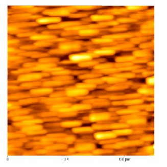
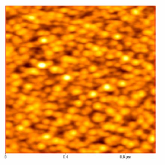
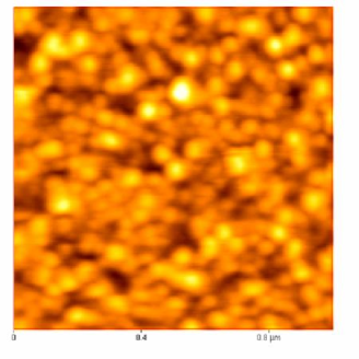
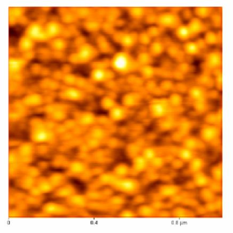
For the unbiased very thin Co layer, Fig. 1a shows a columnar structure of the Co grains grown over the evaporated NiO underlaying surface. However, Fig. 1b shows that by applying the negative bias voltage during the Co deposition, the columnar growth is eliminated. Moreover, Figs. 1c and 1d show that by increasing the bias voltage up to -60 V the grain size of the Co layer is increased which means a more uniform and smoother surface is formed. But, for the bias voltage of -80 V, due to initiation of resputtering of the Co surface by the high energy ion bombardment, we have observed a non-uniform surface, even at the macroscale of the samples. Therefore, based on the AFM micrographs, the optimum surface morphology of the Co/NiO/Si(100) system was achieved at the bias voltage of -60 V for our experimental conditions Sangpour .
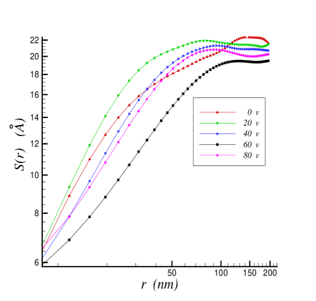
Now, by using the introduced statistical parameters in the last section, it is possible to obtain some quantitative information about the effect of bias voltage on surface topography of the Co/NiO/Si(100) system. Figure 2 presents the structure function of the surface grown at the different bias voltages, using Eq. (8). The slope of each curve at the small scales yields the roughness exponent () of the corresponding surface. Hence, it is seen that the surface grown at the optimum bias voltage (-60 V) shows a minimum roughness with , as compared with the other biased samples with 0.75, 0.70, and 0.64 for V=-20, -40, and -80 V, respectively. For the unbiased sample, we have obtained two roughness exponent values of 0.73 and 0.36, because of the non-isotropic structure of the surface (see Fig. 1a). In any case, at large scales where the structure function is saturated, Fig. 2 shows the maximum and the minimum roughness values for the bias voltages of 0 and -60 V, respectively.
It is also possible to evaluate the grain size dependence to the applied bias voltage, using the correlation length achieved by the structure function represented in Fig. 2. For the unbiased sample, we have two correlation lengths of 30 and 120 nm due to the columnar structure of the grains. However, by applying the bias voltage, we can attribute just one correlation length to each curve showing elimination of the columnar structure in the biased samples. For the bias voltage of -20 V, the correlation length of is found to be 56 nm. By increasing the value of the bias voltage to -40 and -60 V, we have measured =76 and 95 nm, respectively. However, at -80 V, due to initiation of the destructive effects of the high energy ions on the surface, the correlation length is reduced to 76 nm. Now, based on the above analysis, if we assume that Vopt=-60 V, then the roughness exponent and the correlation length can be expressed in terms of the as follows, respectively,
| (16) |
| (17) |
where for with the columnar structure, we have considered the average values.
To obtain the stochastic behavior of the surface, we need to measure the drift coefficient and diffusion coefficient using Eq. (12). Figure 3 shows for the surfaces at the different bias voltages. It can be seen that the drift coefficient shows a linear behavior for as:
| (18) |
where
| (19) |
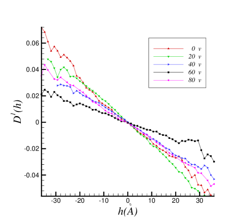
The minimum value of for the biased samples at shows that the deterministic component of the height fluctuations for these samples is lower than the other biased and unbiased ones.
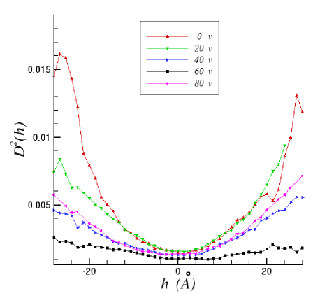
Figure 4 presents for the different bias voltages. At , the maximum value of diffusion has been obtained for any , as compared with the other cases. By increasing the bias voltage, the value of is decreased, as can be seen for and 2/3. The minimum value of , which is nearly independent of , is achieved when . This shows that the noisy component of the surface height fluctuation at is negligible as compared with the unbiased and the other biased samples. The behavior of at becomes similar to its behavior at . It is seen that the diffusion coefficient is approximately a quadratic function of . Using the data analysis, we have found that
| (20) |
where
Now, using the Langevin equation (Eq. (14)) and the measured drift and diffusion coefficients, we can conclude that the height fluctuation has the minimum value at which means a smoother surface at the optimum condition. Moreover, the obtained equations for the coefficients (Eqs. (18) and (20)) can be used to regenerate the rough surfaces the same as AFM images shown in Fig. 1 Jafari ; Waechter .
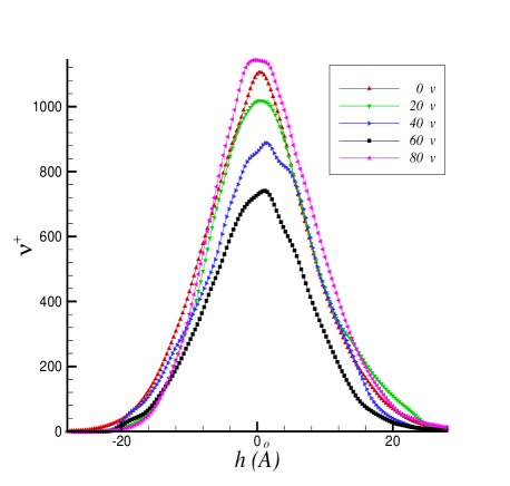
To complete the study, roughness of a surface can be also evaluated by the level crossing analysis, as another procedure. Figure 5 shows the observed average frequency as a function of for the different bias voltages. As is increased from 0 to 1, the value of is decreased at any height. Once again, the optimum situation is observed for the bias voltage of -60 V showing the surface formed at condition is a smoother surface with lower height fluctuations than the surface formed at the other conditions. It is seen that, at , the height fluctuation of the surface finds a maximum value, as compared with the other surfaces. The same as the roughness exponent and the correlation length behavior in terms of , the can be also expressed as:
| (22) |
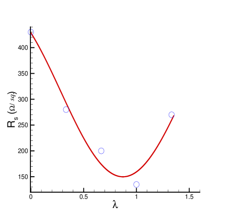
Since the system under investigation has a thin Co layer which is the only conductive layer, thus, it is obvious that lower height fluctuation corresponds to smaller electrical resistivity of the surface. Concerning this, we have measured sheet resistance of the Co surface grown at the different bias voltages, as shown in Fig. 6. For the bias voltage ranging from 0 to -60 V, the Rs value is reduced from 432 to 131 . The minimum value of Rs is measured at the optimum condition of -60 V which can be related to modified and smooth surface roughness. Elimination of interfacial voids as well as porosities, and reduction of impurities in the Co layer. A similar behavior was also observed at Vopt=-50 V for Ta/Si(111) system AkhavanTSF . By increasing the applied bias voltage to values greater than its optimum value, surface roughness is increased because of surface bombardment by high energy ions. This can be seen by the observed increase in the Rs value at the bias voltage of -80 V (). It is easy to examine that the variation of Rs as a function of can be expressed as below:
| (23) |
It behaves similar to the behavior of roughness characteristics of the surfaces. Therefore, we have shown that the roughness behavior explained by the statistical characterizations of the surface, which have been obtained by using microstructural analysis of AFM, can be related to the sheet resistance measurement of rough surfaces, as a macrostructural analysis.
V The tip convolution effect
It is well-known that images acquired with AFM are a convolution of tip and sample interaction. In fact, using scanning probe techniques for determining scaling parameters of a surface leads to an underestimate of the actual scaling dimension, due to the dilation of tip and surface. Concerning this, Aue and Hosson Aue showed that the underestimation of the scaling exponent depends on the shape and aspect ratio of the tip, the actual fractal dimension of the surface, and its lateral vertical ratio. In general, they proved that the aspect ratio of the tip is the limiting factor in the imaging process.
Here, we want to study the aspect ratio effect of the tip on the investigated stochastic parameters. To do this, using a computer simulation program, we have generated a rough surface by using a Brownian motion type algorithm Peitgen ; 24 with roughness and its exponent of 10.00 nm and 0.67, respectively. We have assumed these roughness parameters in order to have some similarity between the generated surface and our analyzed surface by AFM. In the simulation program, the generated surface has been scanned using a sharp cone tip with an assumed aspect ratio of which is also nearly similar to the applied tip in our AFM analysis with the aspect ratio of 0.9. Moreover, this assumption does not limit the generality of our discussion, because it is shown that the fractal behavior of a rough surface presents an independent tip aspect ratio behavior (saturated behavior) for the aspect ratios greater than about 0.4 Aue .
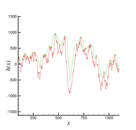
Figure 7 shows a line profile of a generated surface which is dilated by a tip with the known aspect ratio. It is clearly seen that the scanned image (the image affected by the tip convolution) does not completely show the generated surface topography (real surface). Now, it is possible to study the dependance of the examined surface stochastic parameters on the geometrical characteristic of the tip, i.e. aspect ratio.
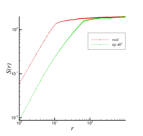
In this regard, Fig. 8 shows variation of the one-dimensional structure function of the generated rough surface due to the tip convolution effect. It can be seen that by increasing the aspect ratio the tip convolution results in obtaining a surface image whit a decreased roughness. Since the aspect ratio of the applied AFM tip was around 0.9, so the measured roughness exponents at the different bias voltages might be corrected by a 1.07 factor. In other words, the relative change (the difference between the real and measured values comparing the real one) of the roughness exponent is about 7.2%.
Moreover, Fig. 8 shows that the correlation length is increased by the tip convolution effect. It should be noted that, in our simulation, we have assumed that the apex of the tip is completely sharp (the tip radius is assumed zero). However, it is well-known that the radius of the pyramidal tips is 20 nm. Therefore, the real correlation lengths are even roughly 20 nm larger than the measured ones by the sharp tip.
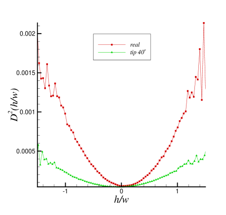
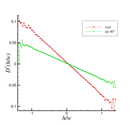
The same tip convolution effect can be also presented for the drift and diffusion coefficients. Figure 9 presents the calculated drift coefficient for the generated surface and the scanned surface. One can see that the tip convolution results in decreasing of the drift coefficient, corresponding to decreasing of the surface roughness. This means that after dilation the correlation length will increase and hence the measured value for would be smaller than its value for the original surface. Therefore, the magnitude of slope of the drift coefficient must decrease after using the tip. For our generated surface, the measured value of the drift coefficient should be modified by a factor of around 2.
The variation of the diffusion coefficient of the generated rough surface due to the tip convolution effect has been also shown in Fig. 10. The reduction of the diffusion coefficient of the scanned surface as compared to its values for the generated surface, due to the tip convolution, can be easily seen. In fact to compensate the tip effect on the diffusion coefficient, we should modify its measured values by a factor of about 4, for the assumed generated surface.
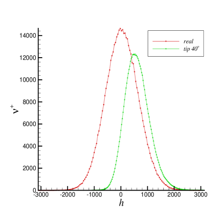
Finally, we remind that the total number of crossing the surface with positive slope () has been defined as a parameter describing the rough surfaces. Hence, we have also studied the effect of the tip convolution on this parameter, as shown in Fig. 11. It is seen that decreased due to the tip convolution effect. For the assumed generated surface, we have obtained that the of the surface before dilation is about 1.7 times larger than its value after the dilation. In this figure, we have also shown the variation of the average height due to the tip effect.
One has to note that our generated surface is a pure two-dimensional one which presents no line-to-line interaction. So, for this simple model, differently shaped tips with the same aspect ratio yield the same results. Therefore, for the three-dimensional case one can expect to obtain a larger distortion of the surface due to stronger line-to-line interaction leading to an even larger underestimation of the studied stochastic parameters.
These analysis showed that, although the measured values of the surface parameters by AFM method are different from the real ones, the general behavior of these parameters as a function of the bias voltage are not affected by the tip convolution. Therefore, our general conclusions about the variation of the studied stochastic parameters by applying the bias voltage is intact.
VI Conclusions
We have investigated the role of bias voltage, as an external parameter, to control the statistical properties of a rough surface. It is shown that at an optimum bias voltage (), the stochastic parameters describing a rough surface such as roughness exponent, level crossing, drift and diffusion coefficient must be found in their minimum values as compared to an unbiased and the other biased samples. In fact, dependence of the height fluctuation of a rough surface to different kinds of the external control parameters, such as bias voltage, temperature, pressure, and so on, can be expressed by AFM data which are analyzed using the surface stochastic parameters. In addition, this characterization enable us to regenerate the rough surfaces grown at the different controlled conditions, with the same statistical properties in the considered scales, which can be useful in computer simulation of physical phenomena at surfaces and interfaces of, especially, very thin layers. It is also shown that these statistical and microstructural parameters can explain well the macroscopic properties of a surface, such as sheet resistance. Moreover, we have shown that the tip-sample interaction does not change the physical behavior of the stochastic parameters affected by the bias voltage.
Acknowledgements.
AZM would like to thank Research Council of Sharif University of Technology for financial support of this work. We also thank F. Ghasemi for useful discussions.References
- (1) A.L. Barabasi and H.E. Stanley, Fractal Concepts in Surface Growth (Cambridge University Press, New York, 1995).
- (2) T. Halpin-Healy and Y.C. Zhang, Phys. Rep. 254, 218 (1995); J. Krug, Adv. Phys. 46, 139 (1997).
- (3) J. Krug and H. Spohn “In Solids Far From Equilibrium Growth, Morphology and Defects”, edited by C. Godreche (Cambridge University Press, New York, 1990).
- (4) P. Meakin Fractals, Scaling and Growth Far From Equilibrium (Cambridge University Press, Cambridge, 1998).
- (5) M. Kardar, Physica A 281, 295 (2000).
- (6) A.A. Masoudi, F. Shahbazi, J. Davoudi, and M. Reza Rahimi Tabar, Phys. Rev. E 65, 026132 (2002).
- (7) G.R. Jafari, S.M. Fazeli, F. Ghasemi, S.M. Vaez Allaei, M. Reza Rahimi Tabar, A. Irajizad, and G. Kavei, Phys. Rev. Lett. 91, 226101 (2003).
- (8) M. Waechter, F. Riess, Th. Schimmel, U. Wendt and J. Peinke, Eur. Phys. J. B 41, 259-277 (2004).
- (9) J. Peinke, M. Reza Rahimi Tabar, and M. Sahimi, Phys. Rev. Lett., submitted, (2004).
- (10) M. Ohring, Materials Science of Thin Films: Deposition and Structure (Academic Press, New York, 2002).
- (11) W.F. Egelhoff, Jr., P.J. Chen, C.J. Powell, M.D. Stiles, R.D. McMichael, C.L. Lin, J.M. Sivertsen, J.H. Judy, K. Takano, A.E. Berkowitz, T.C. Anthony, and J.A. Brug, J. Appl. Phys. 79, 5277 (1996).
- (12) B. Dai, J.N. Coi, and W. Lai, J. Magn. Magn. Mat. 27, 19 (2003).
- (13) A.Z. Moshfegh and O. Akhavan, J. Phys. D 34, 2103 (2001).
- (14) M. Marsilli, A. Maritan, F. Toigoend, and J.R. Banavar, Rev. Mod. Phys. 68, 963 (1996).
- (15) H. Risken, The Fokker-Planck equation (Springer, Berlin, 1984).
- (16) J. Davoudi and M. Reza Rahimi Tabar, Phys. Rev. Lett. 82, 1680 (1999).
- (17) A. Irajizad, G. Kavei, M. Reza Rahimi Tabar, and S.M. Vaez Allaei, J. Phys.: Condens. Matter 15, 1889 (2003).
- (18) A.Z. Moshfegh and O. Akhavan, Thin Solid Films 370, 10 (2000).
- (19) S.N. Majumdar and A.J. Bray, Phys. Rev. Lett. 86, 3700 (2001).
- (20) F. Shahbazi, S. Sobhanian, M. Reza Rahimi Tabar, S. Khorram, G.R. Frootan, and H. Zahed, J. Phys. A 36, 2517 (2003).
- (21) A.Z. Moshfegh and P. Sangpour, Phys. Stat. Sol. C 1, 1744 (2004).
- (22) J. Aue and J.Th.M. De Hosson, Appl. Phys. Lett. 71, 1347 (1997).
- (23) H. Peitgen and D. Saupe, The Science of Fractal Images (Springer, Berlin, 1988).
- (24) J. Peinke, M. Reza Rahimi Tabar, M. sahimi and F. Ghasemi, cond-mat/0411529, (2004).