Scaling of Resistance and Electron Mean Free Path of Single-Walled Carbon Nanotubes
Abstract
We present an experimental investigation on the scaling of resistance in individual single walled carbon nanotube devices with channel lengths that vary four orders of magnitude on the same sample. The electron mean free path is obtained from the linear scaling of resistance with length at various temperatures. The low temperature mean free path is determined by impurity scattering, while at high temperature the mean free path decreases with increasing temperature, indicating that it is limited by electron-phonon scattering. An unusually long mean free path at room temperature has been experimentally confirmed. Exponentially increasing resistance with length at extremely long length scales suggests anomalous localization effects.
Single walled carbon nanotubes (SWNTs) are 1D conductors that exhibit a rich variety of low dimensional charge transport phenomena Dresselhaus1 , including ballistic conduction Kong2 ; Liang3 ; Mann4 ; Javey5 ; Javey6 , localization Navarro7 and 1D variable range hopping Gao8 . The electron mean free path, , is one of the important length scales that characterize the different 1D transport regimes. One method of determining in SWNTs is to measure ballistic conduction for a given device channel length. However, this method yields a lower bound of , and works only at low temperature Kong2 ; Liang3 ; Mann4 ; Javey5 or at higher temperature for small length scales (60 nm) Javey6 . Another approach to obtain at room temperature is to employ scanning probe microscopy to measure the linear scaling of the channel resistance Park9 , or use non-invasive multi-terminal measurements Gao10 . Due to the experimental limitations of these approaches, the characterization of for the same SWNTs over a range of temperatures is yet to be realized.
Recent advances in the growth of extremely long SWNTs (1 mm) Hong11 now allow for an intensive study on their intrinsic properties. In this letter, we present experimental measurements on the scaling behavior of resistance in individual, millimeter long SWNTs for the temperature range of 1.6 - 300 K. From the linear scaling of resistance, the temperature dependent electron mean free path is calculated for each temperature. Beyond the linear scaling regime, we observe that the resistance increases exponentially with length, indicating localization behavior.
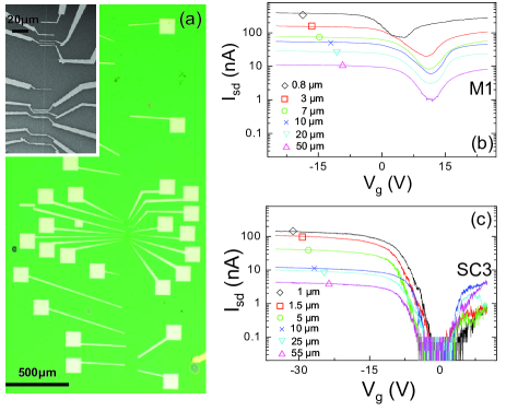
Macroscopically long and straight individual SWNTs were grown on a degenerately doped Si/SiO2 substrate ( 500 nm) using the chemical vapor deposition method described in Ref.Hong11 . This was followed by the fabrication of multiple Pd electrodes with various separations (200 nm- 400 m)(Fig. 1(a)). Pd electrodes were chosen to create highly transparent SWNT-electrode contacts Mann4 . The diameters of the SWNTs were measured by atomic force microscope (AFM). We chose SWNTs with diameter less than 2.5 nm to exclude any possibility of including multiwalled nanotubes (MWNT) in this study. In addition, we confirmed that the high bias saturation current is 30 A for all SWNTs studied Yao12 , assuring that the samples consisted of single tubes rather than small bundles or MWNTs. The substrate was used as a gate electrode to tune the chemical potential of the sample by the application of a gate voltage . A small dc source-drain bias voltage ( 10 mV), , was applied between pairs of consecutive electrodes, and the two-terminal linear response conductance was determined from the measured source-drain current .

Fig. 1(b-c) shows the measured as a function of for selected channel length sections on two representative SWNTs. All curves exhibit a ‘gap’ like feature - a range of where is suppressed. On the same SWNT, every device (pair of consecutive electrodes) shows a similar up to a length-dependent multiplicative factor, once we align the centers of the gap region for each curve. The similarity of the behavior in different sections for each SWNT sample indicates that the corresponding ‘gap’ features are derived from the intrinsic electronic structure of the SWNT rather than the effects of random local variation.
| M1 | M2 | M3 | M4 | SC1 | SC2 | SC3 | SC4 | SC5 | SC6 | SC7 | |
|---|---|---|---|---|---|---|---|---|---|---|---|
| m) | |||||||||||
| m) |
We use the qualitatively different behaviors of different SWNTs to categorize them as metallic (M-NT) or semiconducting nanotubes (S-NT). Typical S-NTs (Fig. 1(c)) exhibit an off current region A when the Fermi energy lies n the energy gap Tans13 ; Appenzeller14 . On the other hand, a weaker suppression of is observed in the ‘small gap’ region in M-NTs (Fig. 1(b)). The ‘small gap’ in M-NTs has been attributed to the curvature-induced energy gap 100 meV Zhou15 , which is distinguished from the S-NT energy gap, which scales with diameter as 1/ (nm) Dresselhaus1 . Among the 11 SWNTs we studied in this letter, we found 4 M-NTs and 7 S-NTs. Each of these SWNTs exhibit a gap centered at , indicating their -doped nature. At large negative gate voltage ( V), lies well outside of the gap region and saturates to , whose value depends only on the applied and channel length of the SWNT section. The two-terminal resistance of the SWNT section is then obtained from . We note that four-terminal resistance measurements are possible for each section by utilizing the available multiple electrode configuration. However, in our experiment, the four terminal measurements yield essentially similar results to the two terminal , which prevents separation of the ‘contact’ resistance contribution from . Such inseparable contact resistance between SWNT-metal electrodes was reported to be caused by the invasiveness of metal contacts Bezryadin16 .

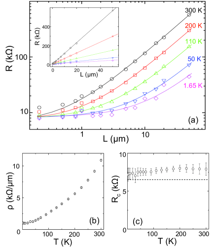
We designed many pairs of electrodes with different on each SWNT so that the scaling of can be studied for a specific sample at a given temperature . Fig. 2(a) show of a representative SWNT measured in the temperature range of 1.6 - 300 K and with an range of 200 nm - 50 m. In these ranges, increases linearly and appears to converge to a finite value for small (inset to Fig. 2(a)). We found that this scaling behavior can be described well by a simple linear dependence with an offset: , where and are interpreted as the 1D resistivity and contact resistance, respectively. The solid lines in Fig. 2(a) are the two parameter line fits of the data points at a given value. From these fits, and are obtained as shown in Fig. 2(b) and Fig. 2(c), respectively. For this sample, remains fairly constant at 8 k and exhibits typical metallic behavior, i.e. it decreases with and saturates to a value at low temperatures. Similar scaling behavior of is observed in other SWNTs, from which both and are extracted within the linear scaling regime. Table 1 summarizes , , and for the 4 M-NTs and 7 S-NTs considered in this study. To understand the scaling of in Fig. 2, we begin with the two-terminal Landauer-Buttiker formula applied to SWNTs Park9 . If we consider 4 low-energy channels in the SWNT, 2 each for spin and band degeneracy, then the scaling of resistance is given by , where and are electron charge and Plank constant and and are the electron mean free path and the non-transparent contact resistance, respectively. Note that we separate out the contribution of from the total contact resistance , so that the contact resistance becomes the quantum resistance when the contacts become fully transparent. From the experimentally obtained and , we can deduce and for each of our SWNT samples. In particular, we note that for the majority of our samples, suggesting that the barrier at the contacts is very thin and adds only a negligible contribution when becomes substantially large.

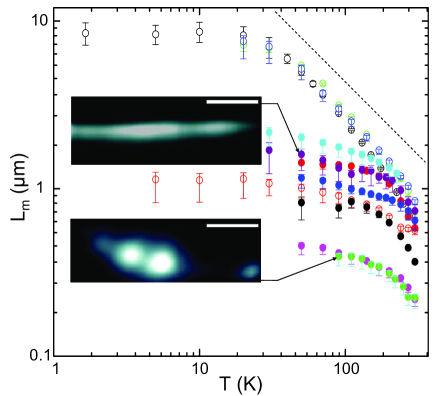
We now discuss the temperature dependent behavior of the mean free path. Fig. 3 is the central result of this letter, showing of the SWNTs listed in Table 1. Overall, exhibits different behaviors in two regimes separated by : (i) the high temperature regime () where (dashed line in Fig. 3), which indicates that inelastic scattering between electrons and acoustic phonons is dominant Park9 ; Avouris17 regardless of chirality Zhou17 ; and (ii) the low temperature regime where saturates to the the tube specific . In this low temperature limit, the phonons freeze out and is determined by the temperature independent elastic scattering with impurities. We believe the widely spread values (0.4-10m) in (ii) are a result of each SWNT sample having a static disorder of different strengths and densities. We employ scanning gate microscopy (SGM) Bachtold18 to image this static disorder. Indeed, the SGM images on S-NTs (insets to Fig. 3) reveal that the SWNT with a shorter shows more defects. Note also that we have experimentally confirmed that is generally much higher for M-NTs than that of S-NTs. This is an indication that the scattering of electrons is strongly suppressed in M-NTs, as predicted by Ando et al. Ando19 and McEuen et al. McEuen20 . In M-NTs we have experimentally shown that the ballistic electron conduction is possible for channel lengths up to 8 m at low temperature and 0.8 m even at room temperature.

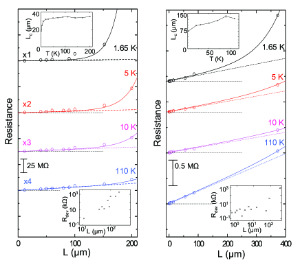
Finally, we turn our attention to the non-linear scaling of . Fig. 4 presents beyond the linear scaling regime of a representative S-NT and M-NT. At extremely long length scales and low temperatures, deviates from the linear dependence extended from the linear regime (dashed lines in main figure and see also in lower insets). Since for all temperatures, we emphasize here that this non-linear behavior in is solely due to increasing electron scattering in the bulk part of the SWNTs rather than an increasing barrier between the SWNT and electrodes. In order to experimentally determine the critical length scale beyond which the non-linear behaviors is dominant, we use a phenomenological equation: to fit the data (solid curves in Fig. 4). While shows a strong sample dependent behavior, generally we found in all temperature ranges, with the temperature dependence exhibiting a trend of increasing with increasing (upper insets to Fig. 4). This observed behavior of excludes the quantum interference related to strong localization effects such as Anderson Localization Navarro7 from the possible scenarios. In particular, in the high temperature regime , the phase coherence length is limited by the phase-breaking electron-phonon scattering, and thus , inviting further study to elucidate the observed localization behavior beyond the strong localization limit Roche21 ; Roche22 .
In conclusion, we determine the length dependent resistance for SWNTs with channel lengths ranged 200 nm - 400m. From the scaling behavior we evaluate the electron mean free path and localization length of the SWNT for a range of temperatures. While the low temperature mean free path is determined by the impurity scattering, an unusually long mean free path is demonstrated at room temperature, even with the dominant electron-phonon scattering.
We thank I. Aleiner, B. Altshuler, and P. Jarillo-Herrero for helpful discussions. This work is supported by the NSF NIRT(ECS 0507111), CAREER (DMR-0349232), NSEC (CHE-0117752), and the New York State Office of Science, Technology, and Academic Research (NYSTAR).
References
- (1) R. Saito, G. Dresselhaus, and M.S. Dresselhaus, Physical Properties of Carbon Nanotubes (Imperial College Press, London 1998).
- (2) J. Kong, E. Yenilmez, T.W. Tombler, W. Kim, H. Dai, R.B. Laughlin, L. Liu, C.S. Jayanthi, and S.Y. Wu, Phys. Rev. Lett. 87, 106801 (2001).
- (3) W. Liang, M. Bockrath, D. Bozovic, J.H. Hafner, M. Tinkham, and H. Park, Nature 411, 665 (2001).
- (4) D. Mann, A. Javey, J. Kong, Q. Wang, and H. Dai, Nano Lett. 3, 1541 (2003).
- (5) A. Javey, J. Guo, Q. Wang, M. Lundstrom and H. Dai, Nature, 424, 654 (2003).
- (6) A. Javey, J. Guo, M. Paulsson, Q. Wang, D. Mann, M. Lundstrom, and H. Dai, Phys. Rev. Lett. 92, 106804 (2004).
- (7) C. Gomez-Navarro, P.J. de Pablo, J. Gomez-Herrero, B. Biel, F.J. Garcia-Vidal, A. Rubio and F. Flores, Nat. Mater. 4, 534 (2005).
- (8) B. Gao, D.C. Glattli, B. Placais and A. Bachtold, Phys. Rev. B 74, 085410 (2006).
- (9) J. Park, S. Rosenblatt, Y. Yaish, V. Sazonova, H. Ustunel, S. Braig, T.A. Arias, P.W. Brouwer and P.L. McEuen, Nano Lett. 4, 517 (2004).
- (10) B. Gao, Y.F. Chen, M.S. Fuhrer, D.C. Glattli, and A. Bachtold, Phys. Rev. Lett. 95, 196802 (2005).
- (11) B.H. Hong, J.Y. Lee, T. Beetz, Y. Zhu, P. Kim, and K.S. Kim, J. Am. Chem. Soc. 127, 15336 (2005).
- (12) Z. Yao, C.L. Kane, and C. Dekker, Phys. Rev. Lett. 84, 2941 (2000).
- (13) S.J. Tans, A.R.M. Verschueren, and C. Dekker, Nature 393, 49 (1998).
- (14) J. Appenzeller, J. Knoch, V. Derycke, R. Martel, S. Wind and Ph. Avouris, Phys. Rev. Lett. 89, 126801 (2002).
- (15) C. Zhou, J. Kong, and H. Dai, Phys. Rev. Lett. 84, 5604 (2000).
- (16) A. Bezryadin, A. R. M. Verschueren, S. J. Tans, and C. Dekker, Phys. Rev. Lett. 80, 4036 (1998).
- (17) V. Perebeinos, J. Tersoff, and Ph. Avouris, Phys. Rev. Lett. 94, 086802 (2005).
- (18) X. Zhou, J. Park, S. Huang, J. Liu, and P. L. McEuen, Phys. Rev. Lett. 95, 146805 (2005).
- (19) A. Bachtold, M.S. Fuhrer, S. Plyasunov, M. Forero, E.H. Anderson, A. Zettl, and P.L. McEuen, Phys. Rev. Lett. 84, 6082 (2000).
- (20) T. Ando and T. Nakanishi, Jpn. J. Appl. Phys. 67, 1704 (1998).
- (21) P.L. McEuen, M. Bockrath, D.H. Cobden, Y. G. Yoon, and S.G. Louie, Phys. Rev. Lett. 83, 5098 (1999).
- (22) F. Triozon, S. Roche, A. Rubio, and D. Mayou, Phys. Rev. B 69, 121410(R) (2004).
- (23) R. Avriller, S. Latil, F. Triozon, X. Balse, and S. Roche, Phys. Rev. B 74, 121406(R) (2006).