Automated Generation of Layout and Control
for Quantum Circuits
Abstract
We present a computer-aided design flow for quantum circuits, complete with automatic layout and control logic extraction. To motivate automated layout for quantum circuits, we investigate grid-based layouts and show a performance variance of four times as we vary grid structure and initial qubit placement. We then propose two polynomial-time design heuristics: a greedy algorithm suitable for small, congestion-free quantum circuits and a dataflow-based analysis approach to placement and routing with implicit initial placement of qubits. Finally, we show that our dataflow-based heuristic generates better layouts than the state-of-the-art automated grid-based layout and scheduling mechanism in terms of latency and potential pipelinability, but at the cost of some area.
1 Introduction
Quantum computing offers us the opportunity to solve certain problems thought to be intractable on a classical machine. For example, the following classically hard problems benefit from quantum algorithms: factorization [19], unsorted database search [6], and simulation of quantum mechanical systems [26].
In addition to significant work on quantum algorithms and underlying physics, there have been several studies exploring architectural trade-offs for quantum computers. Most such research [3, 16] has focused on simulating quantum algorithms on a fixed layout rather than on techniques for quantum circuit synthesis and layout generation. These studies tend to use hand-generated and hand-optimized layouts on which efficient scheduling is then performed. While this approach is quite informative in a new field, it quickly becomes intractable as the size of the circuit grows.
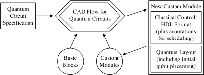
Our goal is to automate most of the tasks involved in generating a physical layout and its associated control logic from a high-level quantum circuit specification (Figure 1). Our computer-aided design (CAD) flow should process a quantum circuit specification and produce the following:
-
•
a physical layout in the desired technology
-
•
an intelligent initial qubit placement in the layout
-
•
classical control circuitry specified in some hardware description language (HDL), which may then be run through a classical CAD flow
-
•
a set of annotations or “hints” for the online scheduler, allowing a tighter coupling of layout optimizations to actual runtime operation
Much like a classical CAD flow, this quantum CAD flow is intended to be used hierarchically. We begin with a set of technology-specific basic blocks (some ion trap technology examples are given in Section 2). We then lay out some simple quantum circuits with the CAD flow, thus creating custom modules. The CAD flow may then be used recursively to create ever larger designs. This approach allows us to develop, evaluate and reuse design heuristics and avoids both the uncertainty and time-intensive nature of hand-generated layouts.
1.1 Motivation for a Quantum CAD Flow
Quantum circuits that are large enough to be “interesting” require the orchestration of hundreds of thousands of physical components. In approaching such problems, it is important to build upon prior work in classical CAD flows. Although the specifics of quantum technologies (such as are discussed in Section 2) are different from classical CMOS technologies, prior work in CAD research can give us insight into how to approach the automated layout of quantum gates and channels.
Further, quantum circuits exhibit some interesting properties that lend themselves to automatic synthesis and computer-aided design techniques:
- Quantum ECC
-
Quantum data is extremely fragile and consequently must remain encoded at all times – while being stored, moved, and computed upon. The encoded version of a circuit is often two or three orders of magnitude larger than the unencoded version. Further, the appropriate level of encoding may need to be selected as part of the layout process in order to achieve an appropriate “threshold” of error-free execution. Rather than burdening the designer with the complexities of adding fault-tolerance to a circuit, computer-aided synthesis, design and verification can perform such tasks automatically.
- Ancillae
-
Quantum computations use many helper qubits known as ancillae. Ancillae consist of bits that are constructed, utilized and recycled as part of a computation. Sometimes, ancillae are explicit in a designer’s view of the circuit. Often, however, they should be added automatically in the process of circuit synthesis, such as during the construction of fault-tolerant circuits from high-level circuit descriptions. An automatic design flow can insert appropriate circuits to generate and recycle ancillae without involving the designer.
- Teleportation
-
Quantum circuits present two possibilities for data transport: ballistic movement and teleportation. Ballistic movement is relatively simple over short distances in technologies such as ion traps (Section 2). Teleportation is an alternative that utilizes a higher-overhead distribution network of entangled quantum bits to distribute information with lower error over longer distances [9]. The choice to employ teleportation is ideally done after an initial layout has determined long communication paths. Consequently, it is a natural target for a computer-aided design flow.
1.2 Contributions
In this paper, we make the following contributions:
-
•
We propose a CAD flow for automated design of quantum circuits and detail the necessary components of the flow.
-
•
We describe a technique for automatic synthesis of the classical control circuitry for a given layout.
-
•
We show that different grid-based architectures, which have been the focus of most prior work in this field, exhibit vastly varying performance for the same circuit.
-
•
We present heuristics for the placement and routing of quantum circuits in ion trap technology.
-
•
We lay out some quantum error correction circuits and evaluate the effectiveness of the heuristics in terms of circuit area and latency.
1.3 Paper Organization
The rest of this paper is organized as follows. We introduce our chosen technology in Section 2, followed by an overview of prior work in the field in Section 3. In Section 4, we detail our proposed CAD flow and our evaluation metrics. In Section 5, we describe the control circuitry interface and scheduling protocol that we use in the following sections. Section 6 contains a study of grid-based layouts, which have been the basis of most prior work on this subject. In Section 7, we present a greedy approach to laying out quantum circuits, followed in Section 8 by a much more scalable dataflow analysis-based approach to layout. Section 9 contains our experimental results for all three approaches to layout generation, and we conclude in Section 10.
2 Ion Traps
For our initial study, we choose trapped ions [4, 17] as our substrate technology. Trapped ions have shown good potential for scalability [10]. In this technology, a physical qubit is an ion, and a gate is a location where a trapped ion may be operated upon by a modulated laser.
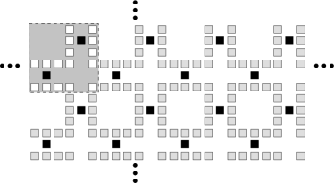
The ion is both trapped and ballistically moved by applying pulse sequences to discrete electrodes which line the edges of ion traps. Figure 3a shows an experimentally-demonstrated layout for a three-way intersection [7]. A qubit may be held in place at any trap region, or it may be ballistically moved between them using the gray electrodes lining the paths.
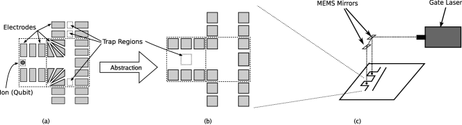
Rather than using ion traps as basic blocks, we define a library of macroblocks consisting of multiple traps for two reasons. First, macroblocks abstract out some of the low-level details, insulating our analyses from variations in the technology implementations of ion traps. Details such as which ion species is used, specific electrode sizing and geometry (clearly variable in the layout in Figure 3a) and exact voltage levels necessary for trapping and movement are all encapsulated within the macroblock. Second, ballistic movement along a channel requires carefully timed application of pulse sequences to electrodes in non-adjacent traps. By defining basic blocks consisting of a few ion traps, we gain the benefit that crossing an interface between basic blocks requires communication only between the two blocks involved.
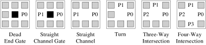
We use the library of macroblocks shown in Figure 2, each of which consists of a 3x3 grid of trap regions and electrodes, with ports to allow qubit movement between macroblocks. The black squares are gate locations, which may not be performed at intersections or turns in ion trap technology. Each of these macroblocks may be rotated in a layout. This library is by no means exhaustive, however it does provide the major pieces necessary to construct many physical circuits. The macroblocks we present are abstractions of experimentally-demonstrated ion trap technology [7, 18]. In Figure 3, we show how one can map a demonstrated layout (Figure 3a) to our macroblock abstractions (Figure 3b). We model this layout as a set of StraightChannel and ThreeWayIntersection macroblocks. Above the ion trap plane is an array of MEMS mirrors which routes laser pulses to the gate locations in order to apply quantum gates [11], as shown in Figure 3c.
Some key differences between this quantum circuit technology and classical CMOS are as follows:
-
•
“Wires” in ion traps consist of rectangular channels, lined with electrodes, with atomic ions suspended above the channel regions and moved ballistically [13]. Ballistic movement of qubits requires synchronized application of voltages on channel electrodes to move data around. Thus each wire requires movement control circuitry to handle any qubit communication.
-
•
A by-product of the synchronous nature of the qubit wire channels is that these circuits can be used in a synchronous manner with no additional overhead. This enables some convenient pipelining options which will be discussed in Section 8.1.
-
•
Each gate location will likely have the ability to perform any operation available in ion trap technology. This enables the reuse gate locations within a quantum circuit.
-
•
Scalable ion trap systems will almost certainly be two-dimensional due to the difficulty of fabricating and controlling ion traps in a third dimension [8]. This means that all ion crossings must be intersections.
-
•
Any routing channel may be shared by multiple ions as long as control circuits prevent multi-ion occupancy. Consequently, our circuit model resembles a general network, although scheduling the movement in a general networking model adds substantial complexity to our circuit.
- •
3 Related Work
Prior research has laid the groundwork for our quantum circuit CAD flow. Svore et al [22, 23] proposed a design flow capable of pushing a quantum program down to physical operations. Their work outlined various file formats and provided initial implementations of some of the necessary tools. Similarly, Balensiefer et al [2, 3] proposed a design flow and compilation techniques to address fault-tolerance and provided some tools to evaluate simple layouts. While our CAD flow builds upon some of these ideas, we concentrate on automatic layout generation and control circuitry extraction.
Additionally, initial hand-optimized layouts have been proposed in the literature. Metodi et al [15] proposed a uniform Quantum Logic Array architecture, which was later extended and improved in [24]. Their work concentrated on architectural research and did not delve into details of physical layout or scheduling. Finally, Metodi et al [16] created a tool to automatically generate a physical operations schedule given a quantum circuit and a fixed grid-based layout structure. We extend and improve upon their work by adding new scheduling heuristics capable of running on grid-based and non-grid-based layouts.
Maslov et al [14] have recently proposed heuristics for the mapping of quantum circuits onto molecules used in liquid state NMR quantum computing technology. Their algorithm starts with a molecule to be used for computation, modeled as a weighted graph with edges representing atomic couplings within the molecule. The dataflow graph of the circuit is mapped onto the molecule graph with an effort to minimize overall circuit runtime. Our techniques focus on circuit placement and routing in an ion trap technology and do not use a predefined physical substrate topology as in the NMR case. A new ion trap geometry is instead generated by our toolset for each circuit.
4 Quantum CAD Flow
The ultimate goal of a quantum CAD flow is identical to that of a standard classical CAD flow: to automate the synthesis and laying out of a circuit. For a quantum CAD flow, the output circuit consists of both the quantum portion and the associated classical control logic.
The quantum CAD flow we present elaborates on the design flows described in prior works [3, 22, 23]. Unlike prior work, our CAD flow addresses the need to integrate automatic generation of classical control into the flow. Figure 4 shows an overview of our CAD toolset. Rectangles are tools, while ovals represent intermediate file formats. Our toolset is built to be as similar to classical CAD flows as possible, while still accounting for the differences between classical and quantum computing described in Section 1.1.
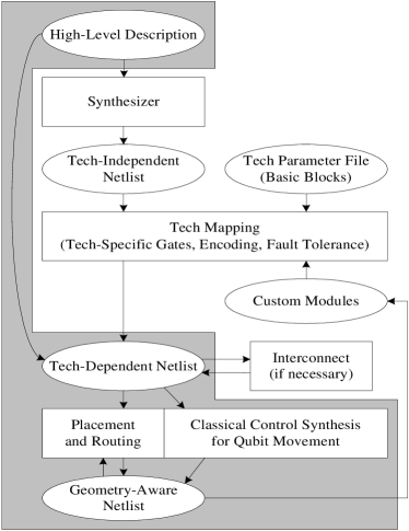
At the top, we begin with a high-level description of the desired quantum circuit. At present this specification consists of a sequence of quantum assembly language (QASM [3]) instructions implementing the desired circuit, since this is a convenient format already being used by various third-party tools. We are currently investigating extension of this high-level description to other formats, such as schematic entry, mathematical formulae or a more general high-level language.
The synthesizer parses the QASM file and generates a technology-independent netlist stored in XML format. From this point onward (downward in the figure), all file formats are XML. Additionally, information may be modified or added but generally not removed. As we move down the flow, we add more and more low level details, but we also keep high-level information such as encoded qubit groupings, nested layout modules, distinction between ancillae and data, etc. This allows low-level tools to make more intelligent decisions concerning qubit placement and channel needs based on high-level circuit structure. It likewise allows logical level modification at the lowest levels without having to attempt to deduce qubit groupings.
A technology parameter file specifies the complete set of basic blocks available for the layout (see examples in Figure 2), as well as design rules for connecting them. A basic block specification contains the following:
-
•
the geometry of the block in enough detail to allow fabrication
-
•
control logic for each operation possible within the block (including both movement and gates)
-
•
control logic for handling each operation possible at each interface
The most basic function of the technology mapping tool is to take a technology-independent netlist and map it onto allowed basic blocks to create the technology-dependent netlist. This may be more or less complicated depending upon the complexity of the basic blocks. In addition, it may need to translate to technology-specific gates (in case the QASM file uses gates not available in this technology), encode the qubits used in the circuit (perhaps also automatically adding the ancilla and operation sequences necessary for error correction) and add fault tolerance to the final physical circuit.
In the initial technology-dependent netlist, all qubits are physical qubits, meaning that encoding levels have been set (though they may still be modified later). At this point, any technology-specific optimizations may optionally be applied to the physical circuit encapsulated in this netlist. Additionally, if the circuit is complex enough to warrant the inclusion of a teleportation-based interconnection network [9], it is added to the netlist here using the higher level qubit grouping information in the netlist.
Once the designer is happy with the netlist, a placement and routing tool lays out the netlist and adds any further channels needed for communication. This geometry-aware netlist may be iterated upon as necessary to refine the layout. Once the layout is finalized, the classical control synthesis tool combines the control logic of the various components of the design, integrates interface control mechanisms to function properly and generates the unified control structure for the entire layout. Our control synthesis tool generates a Verilog file, which may then be run through a classical CAD flow for implementation.
The layout specification along with the control logic file together comprise the geometry-aware netlist, which is the end result for the quantum circuit initially specified in the high-level description. In order to allow hierarchical design of larger quantum circuits, we may now add this geometry-aware netlist to our set of custom modules. Future technology mappings may use both the basic blocks specified in the technology parameter file and any custom modules we create (or acquire).
The gray area in Figure 4 identifies the portions we shall be focusing on for the rest of this paper. We currently process the high-level description (a QASM file) directly into a technology-dependent netlist for ion traps using the macroblocks shown in Figure 2. Thus we perform a tech mapping, but no automatic encoding, interconnect or addition of gates for fault tolerance. In this paper, we focus on laying out low-level circuits, such as those for encoded ancilla generation and error correction. The classical control synthesis box of the CAD flow is discussed in Section 5, while placement and routing are analyzed and compared in Sections 6, 7, 8 and 9.
We use two main metrics to evaluate the performance of our CAD flow: area and latency. For area, we consider the bounding box around the layout, so irregularly-shaped layouts are penalized (since they have wasted space). To determine latency of circuit execution, we use the scheduling heuristic described in Section 5.2 and extended in Section 8.3. A third metric of interest is fault-tolerance. For small layouts and circuits, we can use third-party tools to determine whether a given layout and schedule is fault-tolerant [5], but we do not currently use the fault-tolerance metric in our iterative design flow. We use area and latency because, to a first approximation, lower area and lower latency are likely to decrease decoherence. Previous algorithms to accurately determine the error tolerance of a quantum circuit have involved very computationally-intensive analyses that would be inappropriate for circuits with more than a few dozen gates [1]. However, we are looking into ways to incorporate fault tolerance as a metric.
5 Control
The classical control system is responsible for executing the quantum circuit, including deciding where and when gate operations occur and tracking and managing every qubit in the system. It is composed of the following major components: instruction issue logic, gate control logic and macroblock control logic. Instruction issue logic handles all instruction scheduling and determines qubit movement paths. Gate control logic oversees laser resource arbitration, deciding which requested gate operations may occur at any given time. The macroblock control logic, which consists of an individual logic block for each macroblock in the system, handles all the internals of the macroblock, including details of gate operation for each gate possible within the macroblock, qubit movement within the macroblock and qubit movement into and out of the ports.
5.1 Control Interfaces
The first step in the control flow involves processing the quantum circuit’s high-level description (the QASM file). The instruction issue logic accepts this stream of instructions as input and creates a series of qubit control messages. Using these qubit control messages, macroblock control logic blocks can determine where to move qubits and when to execute a gate operation. Qubit control messages are simple bit streams composed of a qubit ID, along with a sequence of commands, as shown in Figure 5. When a qubit needs to perform an action, the instruction issue logic sends to it an appropriate control message which travels with the qubit as it traverses the layout. Once a macroblock receives a qubit and its corresponding control message, it uses the first command in the sequence to determine the operation it must perform. The macroblock then removes the command bits used and passes on the remaining control message to the next macroblock into which the qubit travels. In this manner, the instruction issue logic can create a multi-command qubit control message that specifies the path a qubit will traverse through consecutive macroblocks, along with where gate operations take place. The instruction issue logic only has to transmit this control message to the source macroblock, relying on the inter-macroblock communication interface to handle the rest.
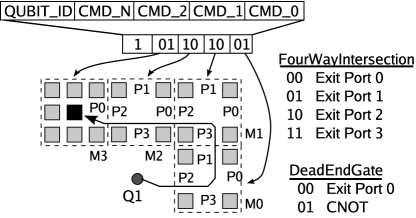
Communication between the instruction issue logic and the macroblocks takes place using a shared control message bus in order to minimize the number of wire connections required by the instruction issue logic. Each macroblock listens to the control message bus for messages addressed to it and only processes messages with a destination ID that match the macroblock’s ID. A macroblock is only responsible for monitoring the control message bus if it contains a qubit that has no remaining command bits. This condition generally occurs after a gate operation, when the instruction issue logic is deciding what action the qubit should take next. Once the instruction issue logic sends a new control message for the qubit, the macroblock resumes operation.
Macroblocks communicate with each other via control signals associated with each quantum port in the macroblock. Each port has signals to control qubit movement into the macroblock and signals to control movement out of the macroblock via that port. These signals are connected to the corresponding signals of the neighboring macroblocks. The macroblocks assert a request signal to a destination macroblock when a qubit command indicates the qubit should cross into the next macroblock. If an available signal response is received, the qubit, along with its control message, can move across into the neighboring macroblock; if not, the qubit must wait until the available signal is present.
The macroblock interface enables the instruction issue logic to schedule qubit movement as a path through a sequence of macroblocks, without concerning itself with the low level details of qubit movement. This modular system allows macroblocks to be replaced with any other macroblock that implements the defined interface, without modifying the instruction issue logic.
Additionally, macroblocks have an interface to the laser control logic. Whenever a macroblock is instructed to perform a gate operation, it must request a laser resource through the laser control logic. The laser controller is responsible for aggregating requests from all the macroblocks in the system, and deciding when and where to send laser pulses. The laser controller also attempts to parallelize as many operations as possible. Once the laser pulses have completed, the laser controller notifies the macroblocks, indicating that the gate operation is complete.
5.2 Instruction Scheduling
The instruction issue logic is responsible for determining the runtime execution order of the instructions in the quantum circuit, which involves both preprocessing and online scheduling. The instruction sequence is first preprocessed to assign priorities that will help during scheduling. The sequence is traversed from end to beginning, scheduling instructions as late as dependencies allow, using realistic gate latencies but ignoring movement. Essentially, each instruction is labeled with the length of its critical path to the end of the program. This is similar to the method used in [16], but we use critical path with gate times rather than the size of the dependent subtree.
The instruction preprocessing generates an optimal schedule assuming infinite gates and zero movement cost. However, we wish to evaluate a layout with more realistic characteristics. Our scheduler is designed to schedule on an arbitrary graph, but the layouts provided to it by the place and route tool are in fact planar layouts using only right angles. In addition, the scheduler requires that the qubit initial positions be provided as well.
Our scheduler implements a greedy scheduling technique. It keeps the set of instructions which have had all their dependencies fulfilled (and thus are ready to be executed). It attempts to schedule them in priority order. So the highest priority ready instruction (according to critical path) is attempted first and is thus more likely to get access to the resources it needs. These contested resources include both gates and channels/intersections. Once all possible instructions have been scheduled, time advances until one or more resources is freed and more instructions may be scheduled. This scheduling and stalling cycle continues until the full sequence has been executed or until deadlock occurs, in which case it is detected and the highest priority unscheduled instruction at the time of deadlock is reported.
Since we are interested in evaluating layouts rather than in designing an efficient online scheduler, we use very thorough searches over the graph in both gate assignment and pathfinding. This causes the scheduler to take longer but takes much of the uncertainty concerning schedule quality out of our tests. In addition, the scheduler reports stalling information which may be used for iterating upon the layout.
5.3 Control Extraction
Armed with well defined component interfaces and a method to execute the quantum instructions, all that remains to create the control system for a given quantum circuit is putting the pieces together. The quantum datapath is composed of an arbitrary number of macroblocks pulled from the component library. Each macroblock in our component library has associated with it classical control logic. The control logic handles all the internals of the macroblock including details of ion movement, ion trapping and gate operation. In our library, the macroblock control logic is specified using behavioral Verilog modules.
When the layout stage of the CAD flow creates a physical layout of macroblocks, we extract the corresponding control logic blocks and assemble them together in a top-level Verilog module for the full control system, stitching together all necessary macroblock interfaces. This module instantiates all the appropriate macroblock control modules, along with the instruction issue logic and laser controller unit. Combined, these modules are assembled into a single Verilog module which implements the full classical control system for the quantum circuit and which may be input to a classical CAD flow for synthesis.
![[Uncaptioned image]](/html/0704.0268/assets/x7.png)
![[Uncaptioned image]](/html/0704.0268/assets/x8.png)
6 Grid-based Layouts
We begin our exploration of placement and routing heuristics by considering grid-based layouts. A majority of the work done in the field has concentrated on these types of layouts. In all of these works, a layout is constructed by first designing a primitive cell and then tiling this cell into a larger physical layout. For example, the authors of [15, 16] manually design a single cell, and for any given quantum circuit, they use that cell to construct an appropriately sized layout. In [23], the authors automate the generation of an H-Tree based layout constructed from a single cell pattern. Similarly, [3] uses a cell such as in [23] but also provides some tools to evaluate the performance of a circuit when the number of communication channels and gate locations within the cell is varied. We use a combination of these methods to implement a tool that automatically creates a grid-based physical layout for a given quantum circuit.
The grid-based physical layouts generated by our tools are constructed by first creating a primitive cell out of the macroblocks mentioned in Section 2 and then tiling the cell to fill up the desired area. For example, Figure 6 shows how a sized cell can be tiled to create the layout used in [16] (referred to henceforth as the QPOS grid). These types of simple structures are easy to automatically generate given only the number of qubits and gate operations in the quantum circuit. Furthermore, grid-based structures are very appealing to consider because, apart from selecting the number of cells in the layout and the initial qubit placement, no other customization is required in order to map a quantum circuit onto the layout. The regular pattern also makes it easy to determine how qubits move through the system, as simple schemes such as dimension-ordered routing can be used.
The approach we use to generate the grid-based layout for a given quantum circuit is as follows:
-
1.
Given the cell size, create a valid cell structure out of macroblocks.
-
2.
Create a layout by tiling the cell to fill up the desired area.
-
3.
Assign initial qubit locations.
-
4.
Simulate the quantum circuit on the layout to determine the execution time.
The first step finds a valid cell structure. A cell is valid if all the macroblocks that open to the perimeter of the cell have an open macroblock to connect to when the cell is tiled. Also, a cell cannot have an isolated macroblock within it that is unreachable. Once we tile this valid cell to create a larger layout, we must decide on how to assign initial qubit locations. The two methods we utilize are: a systematic left to right, one qubit per cell approach, and a randomized placement. The systematic placement allows us to fairly compare different layouts. However, since the initial placement of the qubits can affect the performance of the circuit, the tool also tries a number of random placements in an effort to determine if the systematic placement unfairly handicapped the circuit.
This layout generation and evaluation procedure is iterated upon until all valid cell configurations of the given size are searched. We then repeat this process for different cell sizes. The cell structure that results in the minimum simulated time for the circuit is used to create the final layout.
As an example, Figure 8 shows the results of searching for the best layout composed of sized cells targeting the Golay encode circuit [21], one of our benchmarks shown in Table 1. More than 900 valid cell configurations were tested. For each cell configuration, we try multiple initial qubit placements (as mentioned earlier) resulting in a range of runtimes for each cell configuration. Differences in the runtime of the circuit are not limited to just variations on the cell configuration but are in fact also highly dependent on the initial qubit placement.
Figure 8 shows the best cell structure found by conducting a search of all , , and sized cells for two different circuits. The main result of this search is that the best cell structure used to create the grid-based layout is dependent on what circuit will be run upon it. By varying the location of gates and communication channels, we tailor the structure of the layout to match the circuit requirements.
While this type of exhaustive search of physical layouts is capable of finding an optimal layout for a quantum circuit, it suffers from a number of drawbacks. Namely, as the size of the cell increases, the number of possible cell configurations grows exponentially. Searching for a good layout for anything but the smallest cell sizes is not a realistic option. Furthermore, while small circuits may be able to take advantage of primitive cell based grids, larger circuits will require a less homogeneous layout. One approach to doing this is to construct a large layout out of smaller grid-based pieces, all with different cell configurations. While this approach is interesting, we feel a more promising approach is one that resembles a classical CAD flow, where information extracted from the circuit is used to construct the layout.
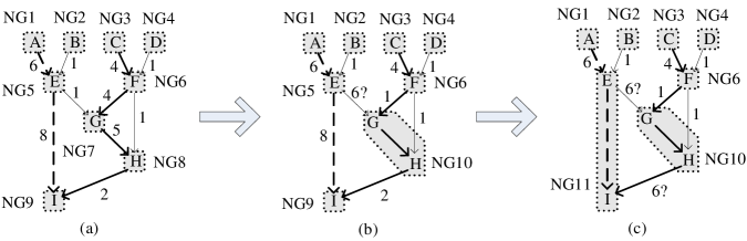
c) We recompute the critical path (A-E-I; dashed bold arrows) and merge its node groups, and so on.
7 Greedy Place and Route
One problem we observed in the regular grid layout design was that the high amount of channel congestion due to limited bandwidth causes densely-packed (occupied) gates. Additionally, we found that a number of gate locations and channels in many of the grids were not even used by the scheduler to perform the circuit.
We present a new heuristic that attempts to solve some of these problems. The heuristic is a simple greedy algorithm that starts with only as many gate locations as qubits (because we assume that qubits only rest in storage/gate locations) and no channels connecting the gates. It iterates with the circuit scheduler, moving and connecting gate locations until the qubits can communicate sufficiently to perform the specified circuit. The current layout is fed into the circuit scheduler which tries to schedule until it finds qubits in gate locations that cannot communicate to perform a gate. The place and router then connects the problematic gate locations and tries scheduling on the layout again. The iteration finishes once the circuit can be successfully completed. Our algorithm bears some similarity to the iterative procedure in adaptive cluster growth placement [12] in classical CAD. Gate locations are placed from the center outward as the circuit grows to fit a rectilinear boundary.
The placer can move gate locations that have to be connected if they are not already connected to something else. The router connects gate locations by making a direct path in the x and y directions between them and placing a new channel, shifting existing channels out of the way. Since channels are allowed to overlap, intersections are inserted where the new channels cut across existing ones.
This technique has the advantage that, since the circuit scheduler prioritizes gates based on gate delay critical path, potentially critical gates are mapped to gate locations and connected early in the process. Thus critical gates tend to be initially placed close together to shorten the circuit critical path. Additionally, gate locations that need to communicate can be connected directly instead of using a general shared grid channel network, where congestion can occur and cause qubits to be routed along unnecessarily long paths.
A disadvantage of this heuristic is that gate placement is done to optimize critical path, not to minimize channel intersections. This means that the layout could end up having many 4-way channel intersections and turns, both of which have more delay than 2-way straight channels. Additionally, even though critical gates are mapped and placed near each other, the channel routing algorithm tends to spread these gate locations apart as more channels cut through the center of the circuit. We discuss our experimental evaluation of this heuristic in Section 9.
8 Dataflow-Based Layouts
As described in Section 6, a systematic row by row initial placement for qubits allows us to make somewhat accurate comparisons between different grid-based layouts, while a random initial qubit placement allows us to test a single grid’s dependence on qubit starting positions. However, in laying out a quantum circuit, we would like to have a more intelligent and natural means of determining initial qubit placement. For this, we turn to the dataflow graph representation of the circuit.
8.1 Dataflow Graph Analysis
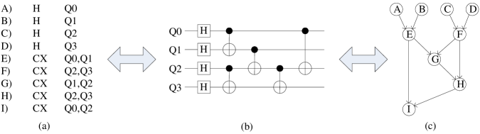
Figure 10a shows a QASM instruction sequence consisting of Hadamard gates (H) and controlled bit-flips (CX) operating on qubits Q0, Q1, Q2 and Q3, with each instruction labeled by a letter. Figure 10b shows the equivalent sequence of operations in standard quantum circuit format. Either of these may be translated into the dataflow graph shown in Figure 10c, where each node represents a QASM instruction (as labeled in Figure 10a) and each arc represents a qubit dependency. With this dataflow graph, we may perform some analyses to help us place and route a layout for our quantum circuit.
The general idea is that we shall create node groups in the dataflow graph which correspond to distinct gate locations that may then be placed and routed on a layout. All instructions within a single node group are guaranteed to be executed at a single gate location, as elaborated upon in Section 8.3. To begin with, we create a node group for each instruction, giving us a dataflow group graph, as shown in Figure 10a. If we lay out this group graph with a distinct designated gate for each instruction (using heuristics discussed in Section 8.2), we get a layout in which the starting location of each qubit is specified implicitly by its first gate location, so no additional initial placement heuristic is needed.
From this layout we can extract movement latency between nodes and label the edges with weights (as in Figure 10a). We now find the longest critical path by qubit. The critical path A-E-I of qubit Q0 has length 14 (the dashed bold arrows), while the critical path C-F-G-H-I of qubit Q2 has length 15 (the solid bold arrows). We select the longest edge on the longest critical path, which is the edge G-H with weight 5. We merge these two node groups to eliminate this latency, in effect specifying that these two instructions should occur at the same gate location (Figure 10b). We then update the layout and recompute distances. Assuming we merged these two node groups to the location of H (NG8), then the weight of edge F-G changes to 1 (to match the weight of edge F-H) and the weight of edge E-G probably changes to 6 (former E-G plus former G-H), but the exact change really depends on layout decisions. The new critical path is now A-E-I, so if we do this again, we merge node groups NG5 and NG9 to eliminate the edge of weight 8, and we get the group graph in Figure 10c.
In merging nodes, there is the possibility that two qubit starting locations get merged, complicating the assignment of initial placement. For this reason, we add a dummy input node for each qubit before its first instruction. The merging heuristic doesn’t allow more than one input node in any single node group, so we maintain the benefit of having an intelligent initial qubit placement without extra work.
There is an important trade-off to consider when taking this merging approach. A tiled grid layout provides plenty of gate location reuse but is unlikely to provide any pipelinability without great effort. A layout of the group graph in Figure 10a (with each instruction assigned to a distinct gate location) provides no gate location reuse at all but high potential pipelinability. This raises the question of whether we wish to minimize area and time (for critical data qubits), maximize throughput of a pipeline (for ancilla generation), or compromise at some middle ground where small sets of nearby nodes are merged in order to exploit locality while still retaining some pipelinability. We intend to further explore this topic in the future.
8.2 Placement and Routing
Taking the group graph from the dataflow analysis heuristic, the placement algorithm takes advantage of the fanout-limited gate output imposed by the No-Cloning Theorem [25] to lay out the dataflow-ordered gate locations in a roughly rectangular block. We adopt a gate array-style design, where gate locations are laid out in columns according to the graph, with space left between each pair of columns for necessary channels. This can lead to wasted space due to a linear layout of uneven column sizes, so we may also perform a folding operation, wherein a short column may be folded in (joined) with the previous column, thus filling out the rectangular bounding box of the layout as much as possible and decreasing area. The columns are then sorted to position gate locations that need to be connected roughly horizontal to one another. This further minimizes channel distance between connected gate locations and reduces the number of high-latency turns.
Once gate locations are placed, we use a grid-based model in which we first route local wire channels between gate locations that are in adjacent or the same columns. These channels tend to be only a few macroblocks long each. A separate global channel is then inserted between each pair of rows and between each pair of columns of gate locations. These global channels stretch the full length of the layout. There are no real routing constraints in our simple model since channels are allowed to overlap and turn into 3- or 4-way intersections. We depend on the dataflow column sorting in the placement phase to reduce the number of intersections and shared local channels. While local channels could technically be used for global routing and vice versa, we’ve found that this division in routing tends to divide the traffic and separate local from long-distance congestion.
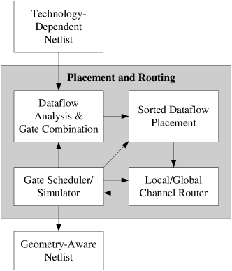
With these basic placement and routing schemes, we may now iterate upon the layout, as shown in Figure 11. The technology-dependent netlist is translated into a dataflow group graph with a separate gate location for each instruction (Figure 10a). This group graph is then placed, routed and scheduled to get latency and identify the runtime critical path (as opposed to the critical path in the group graph, which fails to take congestion into account). The longest latency move on the runtime critical path (between two node groups) is merged into one node group, thus eliminating the move since a node group represents a single gate location. This new group graph is then placed, routed and scheduled again to find the next pair of node groups to merge.
Once this process has iterated enough times, we reach a point where congestion at some heavily merged node group is actually hurting the latency with each further merge. We alleviate this congestion by adding storage nodes (essentially gate locations that don’t actually perform gates) near the congested node group. This increases the area slightly but maintains the locality exploited by the merging heuristic. If congestion persists, we halt the algorithm, back up a few merging steps and output the geometry-aware netlist.
8.3 Annotated Scheduling
The scheduling heuristic described in Section 5.2 schedules an arbitrary QASM instruction sequence on an arbitrary layout. However, once we have assigned instructions in a dataflow graph to node groups (as described in Section 8.1), we wish those instructions to be executed at their proper location on any layout placed and routed from the group graph. To this end, we annotate each instruction in the instruction sequence with the name of the gate location where it must be executed. Additionally, since we have the gate locations in advance, we can incorporate movement in the back-prioritization of the instruction sequence. Thus, the priority assigned to each qubit now incorporates both gate latencies and movement through an uncongested layout, which gives us a better approximation of each qubit’s critical path. We use this extended scheduler in our dataflow-based experiments presented in Section 9.
9 Results
We now present our simulation results for the heuristics described in earlier sections.
9.1 Benchmarks
| Qubit | Gate | |
|---|---|---|
| Circuit name | count | count |
| L1 encode [20] | 7 | 21 |
| L1 encode [21] | 23 | 116 |
| L1 correction [1] | 21 | 136 |
| L2 encode [20] | 49 | 245 |
| Circuit | Heuristic | Latency () | Area |
|---|---|---|---|
| L1 encode | QPOS Grid | 548.0 | 49 |
| Optimal Grid | 509.0 | 49 | |
| Greedy channel and gate location placement | 648.0 | 36 | |
| Non-folded DF, 2 global channels, critical combining | 768.2 | 231 | |
| Folded DF, 1 global channels, critical combining | 795.4 | 126 | |
| Folded DF, 2 global channels, critical combining | 712.4 | 182 | |
| Golay encode | QPOS Grid | 2268.0 | 575 |
| Optimal Grid | 1801.0 | 575 | |
| Greedy channel and gate location placement | 2457.0 | 168 | |
| Non-folded DF, 2 global channels, critical combining | 2169.2 | 3880 | |
| Folded DF, 1 global channels, critical combining | 2264.0 | 713 | |
| Folded DF, 2 global channels, critical combining | 2248.2 | 1394 | |
| L1 correction | QPOS Grid | 1300.0 | 1271 |
| Optimal Grid | 771.0 | 1271 | |
| Greedy channel and gate location placement | 1932.0 | 756 | |
| Non-folded DF, 2 global channels, critical combining | 999.8 | 2378 | |
| Folded DF, 1 global channels, critical combining | 1501.2 | 690 | |
| Folded DF, 2 global channels, critical combining | 1121.2 | 1496 | |
| L2 encode | QPOS Grid | 2411.0 | 1365 |
| Optimal Grid | 1367.0 | 1365 | |
| Greedy channel and gate location placement | 4791.0 | 936 | |
| Non-folded DF, 2 global channels, critical combining | 1582.4 | 4087 | |
| Folded DF, 1 global channels, critical combining | 1828.6 | 1617 | |
| Folded DF, 2 global channels, critical combining | 1944.8 | 3381 |
Relatively high error rates of operations in a quantum computer necessitate heavy encodings of qubits. As such, we focus on encoding circuits (useful for both data and ancillae) and error correction circuits to experiment with circuit layout techniques. We lay out a number of error correction and encoding circuits to evaluate the effectiveness of the heuristics used in our CAD flow in terms of circuit area and latency, as determined by our scheduler. Our circuit benchmarks are shown in Table 1. We use two level 1 (L1) encoding circuits, a level 2 (L2) recursive encoding circuit and a fault-tolerant level 1 correction circuit.
The idea of the encoding circuits is that they will provide a constant stream of encoded ancillae to interact with encoded data qubit blocks. Thus, for these circuits, throughput is a more important measure than latency, implying that they would benefit greatly from pipelining. Nonetheless, a high latency circuit could introduce non-trivial error due to increased qubit idle time. On the other hand, correction circuits are much more latency dependent, since they are on the critical path for the processing of data qubit blocks.
9.2 Evaluation
We have evaluated a variety of layout design heuristics on the four benchmarks shown in Table 1. The results are in Table 2. “QPOS Grid” refers to the best scheduled layout from the literature [16] (see Section 6). “Optimal Grid” refers to the best grid with an area matching the QPOS Grid used that was found by the exhaustive search described in Section 6. “Greedy” refers to the heuristic described in Section 7. “DF” refers to the dataflow-based approach from Section 8. “Non-folded” means the dataflow graph is laid out with varying column widths; “folded” means the layout has been made more rectangular by stacking columns. The number of global channels is between each pair of rows and columns of gate locations. “Critical combining” refers to our dataflow group graph merging heuristic.
The exhaustive search over grids yields the best latency for all benchmarks, which is not surprising. This kind of search becomes intractable quickly as circuit size grows, and additionally, it is based on the unproven assumption that a regular layout pattern is the best approach. We include this data point as something to keep in mind as a target latency.
Among the polynomial-time heuristics, we first note that no single heuristic is optimal for all four benchmarks and that, in fact, no single heuristic optimizes both latency and area for any single circuit. Dataflow-based place and route techniques in general produce the lowest latency circuits. We find that the optimal global channel count per column (1 or 2) depends on the circuit being laid out. This is an artifact of the lack of maturity in our routing methodology. We intend to explore more adaptive routing optimization in our ongoing work.
The dataflow approach and the QPOS Grid tend to trade off between latency and area. However, we expect that the dataflow approach will show greater potential for pipelining, thus allowing us to target circuits such as an encoded ancilla generation factory, for which throughput is of greater importance than latency. We also observe that non-folded dataflow layouts are likely to have even greater pipelinability than folded ones, but at the likely cost of greater area. Although, we should note that the area estimates for the non-folded DF-based layouts are in fact overestimates due to our use of a liberal bounding box for these calculations.
We find that the greedy heuristic tends to find the best design area-wise, but the latency penalty increases with circuit complexity. This is expected, as greedy is unable to handle congestion problems, so it works best for small circuits where congestion is not an issue. It is for the opposite reason that the DF heuristics fail on the L1 encode. They insert too much complexity into an otherwise simple problem.
10 Conclusion
We presented a computer-aided design flow for the layout, scheduling and control of ion trap-based quantum circuits. We focused on physical quantum circuits, that is, ones for which all ancillae, encodings and interconnect are explicitly specified. We explored several mechanisms for generating optimal layouts and schedules for our benchmark circuits.
Prior work has tended to assume a specific regular grid structure and to schedule operations within this structure. We investigated a variety of grid structures and showed a performance variance of a factor of four as we varied grid structure and initial qubit placement. Since exhaustive search is clearly impractical for large circuits, we also explored two polynomial-time heuristics for automated layout design. Our greedy algorithm produces good results for very simple circuits, but quickly begins to be suboptimal as circuit size grows. For larger circuits, we investigated a dataflow-based analysis of the quantum circuit to assist a place and route mechanism which leverages from classical algorithms. We found that our our dataflow approach generally offers the best latency, often at the cost of area. However, we expect that a layout based on the dataflow graph analysis also offers better potential for pipelining than a grid-based approach, and we intend to investigate this further in the future.
References
- [1] P. Aliferis, D. Gottesman, and J. Preskill. Quantum accuracy threshold for concatenated distance-3 codes. Arxiv preprint quant-ph/0504218, 2005.
- [2] S. Balensiefer, L. Kreger-Stickles, and M. Oskin. QUALE: quantum architecture layout evaluator. Proceedings of SPIE, 5815:103, 2005.
- [3] S. Balensiefer, L. Kregor-Stickles, and M. Oskin. An evaluation framework and instruction set architecture for ion-trap based quantum micro-architectures. Proc. 32nd Annual International Symposium on Computer Architecture, 2005.
- [4] J. I. Cirac and P. Zoller. Quantum computations with cold trapped ions. Phys. Rev. Lett, 74:4091–4094, 1995.
- [5] A. Cross. qasm-tools. http://www.media.mit.edu/quanta/quanta-web/projects/qasm-tools/, 2006.
- [6] L. Grover. Symposium on Theory of Computing (STOC 1996), pages 212–219.
- [7] W. Hensinger, S. Olmschenk, D. Stick, D. Hucul, M. Yeo, M. Acton, L. Deslauriers, C. Monroe, and J. Rabchuk. T-junction ion trap array for two-dimensional ion shuttling, storage, and manipulation. Applied Physics Letters, 88(3):34101, 2006.
- [8] D. Hucul, M. Yeo, W. K. Hensinger, J. Rabchuk, S. Olmschenk, and C. Monroe. On the transport of atomic ions in linear and multidimensional ion trap arrays. quant-ph/0702175, 2007.
- [9] N. Isailovic, Y. Patel, M. Whitney, and J. Kubiatowicz. Interconnection Networks for Scalable Quantum Computers. Proceedings of the 33rd International Symposium on Computer Architecture (ISCA), 2006.
- [10] D. Kielpinski, C. Monroe, and D.J. Wineland. Architecture for a large-scale ion-trap quantum computer. Nature, 417:709–711, 2002.
- [11] J. Kim, S. Pau, Z. Ma, H. McLellan, J. Gages, A. Kornblit, and R. Slusher. System design for large-scale ion trap quantum information processor. Quantum Information and Computation, 5(7):515–537, 2005.
- [12] CM Kyung, JM Widder, and DA Mlynski. Adaptive cluster growth (ACG); a new algorithm for circuit packingin rectilinear region. Design Automation Conference, 1990. EDAC. Proceedings of the European, pages 191–195, 1990.
- [13] M.J. Madsen, W.K. Hensinger, D. Stick, J.A. Rabchuk, and C. Monroe. Planar ion trap geometry for microfabrication. Applied Physics B: Lasers and Optics, 78:639 – 651, 2004.
- [14] D. Maslov, S. M. Falconer, and M. Mosca. Quantum circuit placement: Optimizing qubit-to-qubit interactions through mapping quantum circutis into a physical experiment. quant-ph/0703256, 2007.
- [15] T. Metodi, D. Thaker, A. Cross, F. Chong, and I. Chuang. A Quantum Logic Array Microarchitecture: Scalable Quantum Data Movement and Computation. Proceedings of the 38th International Symposium on Microarchitecture (MICRO), 2005.
- [16] T.S. Metodi, D.D. Thaker, A.W. Cross, F.T. Chong, and I.L. Chuang. Scheduling physical operations in a quantum information processor. Proceedings of SPIE, 6244:62440T, 2006.
- [17] C. Monroe, D. M. Meekhof, B. E. King, W. M. Itano, and D. J. Wineland. Demonstration of a universal quantum logic gate. Phys. Rev. Lett., 75:4714–4717, 1995.
- [18] C. Pearson, D. Leibrandt, W. Bakr, W. Mallard, K. Brown, and I. Chuang. Experimental investigation of planar ion traps. Phys. Rev. A, 73(3), 2006.
- [19] P.W. Shor. Polynomial-time algorithms for prime factorization and discrete logarithms on a quantum computer. 35’th Ann. Symp. on Foundations of Comp. Science (FOCS), pages 124–134, 1994.
- [20] A. M. Steane. Simple quantum error correcting codes. Phys. Rev. A, 54:4741–4751, 1996.
- [21] A.M. Steane. Overhead and noise threshold of fault-tolerant quantum error correction. Phys. Rev. A, 68(4):42322, 2003.
- [22] K. Svore, A. Aho, A. Cross, I. Chuang, and I. Markov. A Layered Software Architecture for Quantum Computing Design Tools. Computer, 39(1):74–83, 2006.
- [23] K. Svore, A. Cross, A. Aho, I. Chuang, and I. Markov. Toward a software architecture for quantum computing design tools. Proceedings of the 2nd International Workshop on Quantum Programming Languages (QPL), pages 145–162, 2004.
- [24] D.D. Thaker, T.S. Metodi, A.W. Cross, I.L. Chuang, and F.T. Chong. Quantum Memory Hierarchies: Efficient Designs to Match Available Parallelism in Quantum Computing. Proceedings of the 33rd International Symposium on Computer Architecture (ISCA), 2006.
- [25] W. Wootters and W. Zurek. A single quantum cannot be cloned. Nature, 299:802–803, 1982.
- [26] C. Zalka. Simulating quantum systems on a quantum computer. Proceedings: Mathematical, Physical and Engineering Sciences, 454(1969):313–322, 1998.