Half-metallic silicon nanowires
Abstract
From first-principles calculations, we predict that transition metal (TM) atom doped silicon nanowires have a half-metallic ground state. They are insulators for one spin-direction, but show metallic properties for the opposite spin direction. At high coverage of TM atoms, ferromagnetic silicon nanowires become metallic for both spin-directions with high magnetic moment and may have also significant spin-polarization at the Fermi level. The spin-dependent electronic properties can be engineered by changing the type of dopant TM atoms, as well as the diameter of the nanowire. Present results are not only of scientific interest, but can also initiate new research on spintronic applications of silicon nanowires.
pacs:
73.22.-f, 68.43.Bc, 73.20.Hb, 68.43.FgRod-like, oxidation resistant Si nanowires (SiNW) can now be fabricated at small diametersma (1-7 nm) and display diversity of interesting electronic properties. In particular, the band gap of semiconductor SiNWs varies with their diameters. They can serve as a building material in many of electronic and optical applications like field effect transistors Cui (FETs), light emitting diodes Huang , lasers Duan and interconnects. Unlike carbon nanotubes, the conductance of semiconductor nanowire can be tuned easily by doping during the fabrication process or by applying a gate voltage in a SiNW FET.
In this letter, we report a novel spin-dependent electronic property of hydrogen terminated silicon nanowires (H-SiNW): When doped by specific transition metal (TM) atoms they show half-metallicgroot ; pickett (HM) ground state. Namely, due to broken spin-degeneracy, energy bands and split and the nanowire remains to be insulator for one spin-direction of electrons, but becomes a conductor for the opposite spin-direction achieving 100% spin polarization at the Fermi level. Under certain circumstances, depending on the dopant and diameter, semiconductor H-SiNWs can be also either a ferromagnetic semiconductor or metal for both spin directions. High-spin polarization at the Fermi level can be achieved also for high TM coverage of specific SiNWs. Present results on the asymmetry of electronic states of TM doped SiNWs are remarkable and of technological interest since room temperature ferromagnetism is already discovered in Mn-doped SiNWwu . Once combined with advanced silicon technology, these properties can be realizable and hence can make ”known silicon” again a potential material with promising nanoscale technological applications in spintronics, magnetism.
Even though 3D ferromagnetic Heusler alloys and transition-metal oxides exhibit half-metallic properties park , they are not yet appropriate for spintronics because of difficulties in controlling stoichiometry and the defect levels destroying the coherent spin-transport. Qian et al. have proposed HM heterostructures composed of -doped Mn layers in bulk Si fong . Recently, Son et al. cohen predicted HM properties of graphene nanoribbons. Stable 1D half-metals have been also predicted for TM atom doped arm-chair single-wall carbon nanotubes yang and linear carbon chains sefa ; engin ; but synthesis of these nanostructures appears to be difficult.
Our results are obtained from first-principles plane wave calculations vasp (using a plane-wave basis set up to kinetic energy of 350 eV) within generalized gradient approximation expressed by PW91 functionalgga . All calculations for paramagnetic, ferromagnetic and antiferromagnetic states are carried out using ultra-soft pseudopotentials vanderbilt and confirmed by using PAW potentialblochl . All atomic positions and lattice constants are optimized by using the conjugate gradient method where total energy and atomic forces are minimized. The convergence for energy is chosen as 10-5 eV between two steps, and the maximum force allowed on each atom is 0.05 eV/Ådetail .
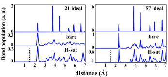
Bare SiNW(N)s (which are oriented along [001] direction and have N Si atoms in their primitive unit cell) are initially cut from the ideal bulk Si crystal in rod-like forms and subsequently their atomic structures and lattice parameter are relaxed sinw . The optimized atomic structures are shown for N=21, 25, and 57 in Fig. 2. While bare SiNW(21) is a semiconductor, bare SiNW(25) and SiNW(57) are metallic. The average cohesive energy relative to a free Si atom () is comparable with the calculated cohesive energy of bulk crystal (4.64 eV per Si atom) and it increases with increasing N. The average cohesive energy relative to the bulk Si crystal, , is small but negative as expected. Upon passivation of dangling bonds with hydrogen atoms all of these SiNWs (specified as H-SiNW) become semiconductor with a band gap . The binding energy of adsorbed hydrogen relative to the free H atom (), as well as relative to the free H2 () are both positive and increases with increasing N. Extensive ab initio molecular dynamics calculations have been carried out at 500 K using supercells, which comprise either two or four primitive unit cells of nanowires to lift artificial limitations imposed by periodic boundary condition. After several iterations lasting 1 ps, the structure of all SiNW(N) and H-SiNW(N) remained stable. Even though SiNWs are cut from ideal crystal, their optimized structures deviate substantially from crystalline coordination, especially for small diameters as seen in Fig.1. Upon hydrogen termination the structure is healed substantially, and approaches the ideal case with increasing N (or increasing diameter), as expected. The calculated response of the wire to a uniaxial tensile force, , ranging from 172 to 394 eV/cell indicates that the strength of H-SiNW(N)s (N=21-57) is rather high.
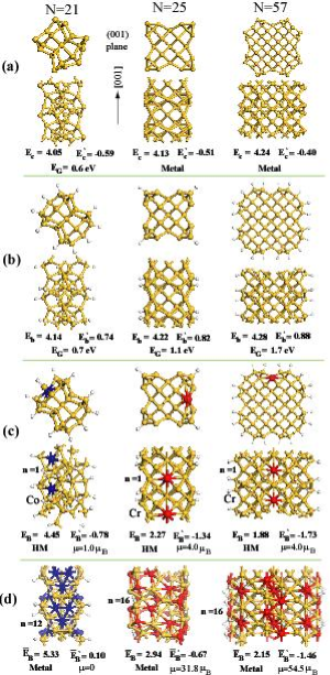
The adsorption of a single TM (TM=Fe, Ti, Co, Cr, and Mn) atom per primitive cell, denoted by , have been examined for different sites (hollow, top, bridge etc) on the surface of H-SiNW(N) for N=21, 25 and 57. In Fig. 2(c) we present only the most energetic adsorption geometry for a specific TM atom for each N, which results in a HM state. These are Co-doped H-SiNW(21), Cr-doped SiNW(25) and Cr-doped SiNW(57). These nanowires have ferromagnetic ground state, since their energy difference between calculated spin-unpolarized and spin-polarized total energy, i.e. is positive. We calculated 0.04, 0.92 and 0.94 eV for H-SiNW(21)+Co, H-SiNW(25)+Cr and H-SiNW(57)+Cr, respectively magnet . Moreover, these wires have the integer number of unpaired spin in their primitive unit cell. In contrast to usually weak binding of TM atoms on single-wall carbon nanotubes which can lead to clustering engin2 , the binding energy of TM atoms () on H-SiNWs is high and involve significant charge transfer from TM atom to the wire binding . Mulliken analysis indicates that the charge transfer from Co to H-SiNW(21) is 0.5 electrons. The charge transfer from Cr to H-SiNW(25) and H-SiNW(57) is even higher (0.8 and 0.9 electrons, respectively). Binding energies of adsorbed TM atoms relative to their bulk crystals () are negative and hence indicate endothermic reaction. Due to very low vapor pressure of many metals, it is probably better to use some metal-precursor to synthesize the structures predicted here.
The band structures of HM nanowires are presented in Fig.3. Once a Co atom is adsorbed above the center of a hexagon of Si atoms on the surface of H-SiNW(21) the spin degeneracy is split and whole system becomes magnetic with a magnetic moment of =1 (Bohr magneton per primitive unit cell). Electronic energy bands become asymmetric for different spins: Bands of majority spins continue to be semiconducting with relatively smaller direct gap of =0.4 eV. In contrast, two bands of minority spins, which cross the Fermi level, become metallic. These metallic bands are composed of Co- and Si- hybridized states with higher Co contribution. The density of majority and minority spin states, namely and , display a 100% spin-polarization at . Cr-doped H-SiNW(25) is also HM. Indirect gap of majority spin bands has reduced to 0.5 eV. On the other hand, two bands constructed from Cr- and Si- hybridized states cross the Fermi level and hence attribute metallicity to the minority spin bands. Similarly, Cr-doped H-SiNW(57) is also HM. The large direct band gap of undoped H-SiNW(57) is modified to be indirect and is reduced to 0.9 eV for majority spin bands. The minimum of the unoccupied conduction band occurs above but close to the Fermi level. Two bands formed by Cr- and Si- hybridized states cross the Fermi level. The net magnetic moment is 4 . Using PAW potential results, we estimated Curie temperature of half-metallic H-SiNW+TMs as 8, 287, and 709 K for N=21, 25, and 57, respectively.
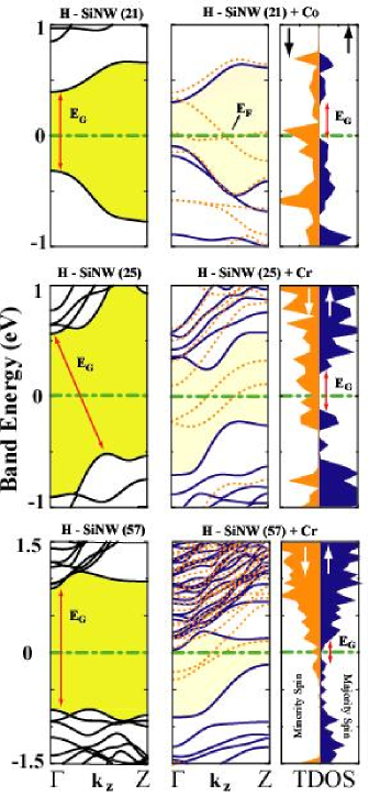
The well-known fact that density functional theory underestimates the band gap, does not concern the present HM states, since H-SiNWs are already verified to be semiconductor experimentallyma and upon TM-doping they are predicted to remain semiconductor for one spin direction. In fact, band gaps predicted here are in fair agreement with experiment and theory. As for partially filled metallic bands of the opposite spin, they are properly represented. Under uniaxial compressive strain the minimum of the conduction band of majority spin states rises above the Fermi level. Conversely, it becomes semi-metallic under uniaxial tensile strain. Since conduction and valence bands of both H-SiNW(21)+Co and H-SiNW(25)+Cr are away from , their HM behavior is robust under uniaxial strain. Also the effect of spin-orbit coupling is very small and cannot destroy HM properties sefa . The form of two metallic bands crossing the Fermi level eliminates the possibility of Peierls distortion. On the other hand, HM ground state of SiNWs is not common to all TM doping. For example H-SiNW(N)+Fe is consistently ferromagnetic semiconductor with different and . H-SiNW(N)+Mn(Cr) can be either ferromagnetic metal or HM depending on N.
To see whether spin-dependent GGA properly represents localized -electrons and hence possible on-site repulsive Coulomb interaction destroys the HM, we also carried out LDA+U calculationsldau . We found that insulating and metallic bands of opposite spins coexist up to high values of repulsive energy () for N=25. For N=57, HM persists until U1. Clearly, HM character of TM doped H-SiNW revealed in Fig.3 is robust and unique behavior.
Finally, we note that HM state predicted in TM-doped H-SiNWs occurs in perfect structures; complete spin-polarization may deviate slightly from P=100% due to the finite extent of devices. Even if the exact HM character corresponding to is disturbed for , the possibility that some H-SiNWs having high spin-polarization at at high TM coverage can be relevant for spintronic applications. We therefore investigated electronic and magnetic structure of the above TM-doped H-SiNWs at as described in Fig. 2(d). Figure 4 presents the calculated density of minority and majority spin states of Cr covered H-SiNWs.
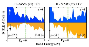
It is found that H-SiNW(21) covered by Co is non-magnetic for both coverage of and 12. H-SiNW(25) is, however, ferromagnetic for different level of Cr coverage and has high net magnetic moment. For example, can be achieved by two different geometries; both geometries are ferromagnetic with =19.6 and 32.3 and are metallic for both spin directions. Interestingly, while is negligible for the former geometry, the latter one has and hence is suitable for spintronic applications (See Fig. 4). Similarly, Cr covered H-SiNW(57) with and 16 are both ferromagnetic with = 34.3 (56) and =54.5 (0.33), respectively. The latter nanostructure having magnetic moment as high as 54.5 can be a potential nanomagnet. Clearly, not only total magnetic moment, but also the spin polarization at of TM covered H-SiNMs exhibits interesting variations depending on , N and the type of TM.
In conclusion, hydrogen passivated SiNWs can exhibit half-metallic state when doped with certain TM atoms. Resulting electronic and magnetic properties depend on the type of dopant TM atom, as well as on the diameter of the nanowire. As a result of TM- and Si- hybridization two new bands of one type of spin direction are located in the band gap, while the bands of other spin-direction remain to be semiconducting. Electronic properties of these nanowires depend on the type of dopant TM atoms, as well as on diameter of the H-SiNW. When covered with more TM atoms, perfect half-metallic state of H-SiNW is disturbed, but for certain cases, the spin polarization at continues to be high. High magnetic moment obtained at high TM coverage is another remarkable result which may lead to the fabrication of nanomagnets for various applications. Briefly, functionalizing silicon nanowires with TM atoms presents us a wide range of interesting properties, such as half-metals, 1D ferromagnetic semiconductors or metals and nanomagnets. We believe that our findings hold promise for the use of silicon -a unique material of microelectronics- in nanospintronics including magnetoresistance, spin-valve and non-volatile memories.
References
- (1) D. D. D. Ma et al., Science 299, 1874 (2003).
- (2) Y. Cui, Z. Zhong, D. Wang, W. U. Wang and C. M. Lieber, Nano Lett. 3, 149 (2003).
- (3) Y. Huang, X. F. Duan and C. M. Lieber, Small 1, 142 (2005).
- (4) X. F. Duan, Y. Huang, R. Agarwal and C. M. Lieber, Nature(London) 421, 241 (2003).
- (5) R.A. de Groot et al., Phys. Rev. Lett. 50, 2024 (1983).
- (6) W.E. Pickett and J. S. Moodera, Phys. Today 54, 39 (2001).
- (7) J.-H. Park et al., Nature (London) 392, 794 (1998).
- (8) W.H. Wu, J.C. Tsai and J.L. Chen, Appl. Phys. Lett. 90, 043121 (2007).
- (9) M.C. Qian et al., Phys. Rev. Lett. 96, 027211 (2006).
- (10) Y-W Son, M.L. Cohen and S.G. Louie, Nature 444, (2006); Phys. Rev. Lett. 97, 216803 (2006).
- (11) C. Yang, J. Zhao and J.P. Lu, Nano. Lett. 4, 561 (2004); Y. Yagi et al., Phys. Rev. B 69, 075414 (2004).
- (12) S. Dag et al., Phys. Rev. B 72, 155444 (2005).
- (13) E. Durgun et al., Europhys. Lett. 73, 642 (2006).
- (14) Numerical computations have been carried out by using VASP software: G. Kresse, J. Hafner, Phys Rev. B 47, R558 (1993). Calculations of charge transfer, orbital contribution and local magnetic moments have been repeated by SIESTA code using local basis set, P. Ordejon, E. Artacho and J.M. Soler, Phys. Rev. B 53, R10441 (1996).
- (15) J. P. Perdew et al., Phys. Rev. B 46, 6671 (1992).
- (16) D. Vanderbilt, Phys. Rev. B 41, R7892 (1990).
- (17) P.E. Bloechl, Phys. Rev. B 50, 17953 (1994).
- (18) All structures have been treated within supercell geometry using the periodic boundary conditions with lattice constants of and ranging from 20 Å to 25 Å depending on the diameter of the SiNW and ( being the optimized lattice constant of SiNW along the wire axis). Some of the calculations have been carried out in double and quadruple primitive unit cells of SiNW by taking and , respectively. In the self-consistent potential and total energy calculations the Brillouin zone is sampled in the k-space within Monkhorst-Pack scheme [H.J. Monkhorst and J.D. Pack, Phys. Rev. B 13, 5188 (1976)] by (1x1x15) mesh points.
- (19) Numerous theoretical studies on SiNW have been published in recent years. See for example: A. K. Singh et al., Nano. Lett. 6, 920 (2006); Q. Wang et al., Phys. Rev. Lett. 95, 167200 (2005); Nano Lett. 5, 1587 (2005).
- (20) Spin-polarized calculations have been carried by relaxing the magnetic moment and by starting with different initial values. Whether antiferromagnetic ground state exists in H-SiNW(N)+TM’s has been explored by using supercell including double primitive cells.
- (21) E. Durgun et al., Phys. Rev. B 67, 201401(R) (2003); J. Phys. Chem. B 108, 575 (2004).
- (22) Binding energy corresponding to =1 is calculated by the following expression, in terms of the total energy of optimized H-SiNW(N) and TM-doped H-SiNW(N) (i.e. H-SiNW(N)+TM) and the total energy of the string of TM atoms having the same lattice parameter of H-SiNW(N)+TM, all calculated in the same superlattice. Hence can be taken as the binding energy of single isoalted TM atom, since the coupling amaong adsorbed TM atoms has been excluded. To calculate , is taken as the total energy of bulk TM crystal per atom. For ¿1, (TM) is taken as the free TM atom energy, and hence includes the coupling between TM atoms. For this reason for H-SiNW(21)+Co at =12
- (23) S.L. Dudarev et al., Phys. Rev. B, 57, 1505 (1998).