Interband polarized absorption in InP polytypic superlattices
Abstract
Recent advances in growth techniques have allowed the fabrication of semiconductor nanostructures with mixed wurtzite/zinc-blende crystal phases. Although the optical characterization of these polytypic structures is well reported in the literature, a deeper theoretical understanding of how crystal phase mixing and quantum confinement change the output linear light polarization is still needed. In this paper, we theoretically investigate the mixing effects of wurtzite and zinc-blende phases on the interband absorption and in the degree of light polarization of an InP polytypic superlattice. We use a single 88 kp Hamiltonian that describes both crystal phases. Quantum confinement is investigated by changing the size of the polytypic unit cell. We also include the optical confinement effect due to the dielectric mismatch between the superlattice and the vaccum and we show it to be necessary to match experimental results. Our calculations for large wurtzite concentrations and small quantum confinement explain the optical trends of recent photoluminescence excitation measurements. Furthermore, we find a high sensitivity to zinc-blende concentrations in the degree of linear polarization. This sensitivity can be reduced by increasing quantum confinement. In conclusion, our theoretical analysis provides an explanation for optical trends in InP polytypic superlattices, and shows that the interplay of crystal phase mixing and quantum confinement is an area worth exploring for light polarization engineering.
I Introduction
The past few years has seen tremendous advances in growth techniques of low dimensional semiconductor nanostructures, especially concerning III-V nanowires (NWs). At the moment, it is possible to precisely tune the growth conditions to achieve single crystal phase nanostructuresMohan, Motohisa, and Fukui (2005); Vu et al. (2013); Pan et al. (2014) or polytypic heterostructures with sharp interfacesLehmann et al. (2013); Khranovskyy et al. (2013). Moreover, it has been reported successful integration of III-V NWs with siliconRen et al. (2013); Borg et al. (2014); Heiss et al. (2014); Li et al. (2014), increasing the possibilities for developing new optoelectronic devicesAkopian et al. (2010); Smit et al. (2014).
Because of its lower surface recombination and higher electron mobilityJoyce et al. (2013); Ponseca et al. (2014), InP is a good candidate, among the III-V compounds, to be embedded in these novel devices. Polytypic InP homojunctions showing a type-II band alignmentMurayama and Nakayama (1994) can be explored to engineer light polarizationBa Hoang et al. (2010) and to enhance the lifetime of carriersPemasiri et al. (2009); Yong et al. (2013). In fact, the use of InP NWs has been proposed in FETsDuan et al. (2001); Jiang et al. (2007); Wallentin et al. (2012), silicon integrated nanolasersWang et al. (2013) and stacked p-n junctions in solar cellsWallentin et al. (2013); Cui et al. (2013).
Although the process underlying the formation of these polytypic homojunctions is elucidatedAkiyama, Nakamura, and Ito (2006); Kitauchi et al. (2010); Ikejiri et al. (2011); Poole et al. (2012) and an extensive literature on the optical characterization of these structures is availableMattila et al. (2006); Mishra et al. (2007); Paiman et al. (2009); Gadret et al. (2010); Kailuweit et al. (2012); Li et al. (2014), we lack theoretical understanding of how the crystal phase mixture changes the light polarization on these nanostructures.
The aim of this study is to provide a comprehensive analysis on how wurtzite (WZ)/zinc-blende (ZB) mixing, quantum confinement (QC), and also optical confinement (OC) modify the interband absorption and the degree of linear polarization (DLP) in an InP polytypic superlattice. From now on, we will use the term superlattice for the polytypic case. In our calculations, the QC along growth direction takes into account the changes of WZ and ZB phases. Also, assuming large crosssections, we neglect lateral QC.
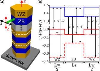
A scheme of the superlattice and possible light polarizations is presented in Fig. 1(a). Although we show a NW with multiple WZ and ZB segments, the periodicity of these segments allows us to consider only the unit cell, bounded by dashed lines, to understand the physics of the superlattice. The incoming light polarization can be either parallel (Z) or perpendicular (X) to the growth direction.
To calculate the band structure, we extend our polytypic kp methodFaria Junior and Sipahi (2012) and include the conduction and valence band interaction explicitly. This interaction increases the reliability of the method, and allows us to calculate the band structure further away from the center of the Brillouin zone. Furthermore, we provide the parameter sets for WZ and ZB InP in this new 88 kp configuration.
We find that the trends of recent photoluminescence (PL) and excitation photoluminescence (PLE) measurements performed by Gadret et al.Gadret et al. (2010) can be explained by our model. Although their samples are disordered, i.e., the regions of WZ/ZB are not periodically ordered, we can predict the observed trends considering a supercell of 100 nm composed of 95% WZ. In addition, we show that the DLP can be tuned using WZ/ZB mixing and QC. The limiting cases of our superlattice, i.e., pure ZB and pure WZ NWs are also calculated and their DLP around gap energy is in very good agreement with the results from Mishra et al. Mishra et al. (2007). This matching emphasizes the use of OC in our calculations.
The structure of the present paper is the following: in Sec. II, we describe the 88 polytypic kp method and present our approach for the interband transitions. Section III contains our results for interband absorption and DLP in the bulk and superlattice regimes. Finally, in Sec. IV, we summarize our main findings and present our conclusions.
II Theoretical background
II.1 Hamiltonian
We expand the Hamiltonian of Ref.Faria Junior and Sipahi (2012) to explicitly include the interband interaction. Since there is no coupling between the ZB irreducible representations for conduction () and valence () bands, we can apply the same rotationPark and Chuang (2000) for the [001] kp matrix with interband interaction. The total rotation matrix would be the direct sum of valence and conduction band rotation matrices, therefore an 88 matrix with 66 and 22 blocks. An alternative procedure would be to start with the Hamiltonian in the [111] coordinate system without interband interaction and derive the interband matrix elements in the [111] coordinate system relating them to the [001].
Our bulk Hamiltonian basis set, defined at -point, in the ZB[111]/WZ[0001] coordinate system is:
| (1) |
with 1-6 representing the valence band states and 7-8 the conduction band states. In this basis set, the Hamiltonian including interband interactions is given by
| (2) |
where represent the valence band, the conduction band and the interaction term between them. The sub-matrices have the following forms:
| (3) |
| (4) |
| (5) |
and their terms
| (6) |
where and , given in units of , are the effective mass parameters of valence and conduction band, respectively. Here is the crystal field splitting energy in WZ, are the spin-orbit coupling splitting energies, and are the Kane parameters of the interband interactions, given by
| (7) |
We would like to emphasize that the Hamiltonian (2) and its terms (6) describe both WZ and ZB crystal structures, however, the usual ZB parameters must be mapped to the ones in equation (6). Moreover, the inclusion of the interband interaction explicitly in the Hamiltonian also requires some corrections to be made in the second order effective mass parameters. These corrections appear because conduction and valence band states are now treated as belonging to the same class, following Löwdin’s notation Löwdin (1951). We describe the mapping and corrections of parameters with detail in Appendix A.
In order to treat the confined direction along , we apply the envelope function approximationBastard (1981); Baraff and Gershoni (1991) to the Hamiltonian (2). This treatment can be summarized with the following changes:
| (8) |
with representing the parameters in the Hamiltonian (different in WZ and ZB), representing an effective mass parameter and is the interband parameter. The last two equations are the symmetrization requirements to hold the Hermitian property of the momentum operatorBaraff and Gershoni (1991). Any parameter in the Hamiltonian acquires a dependence along , making it different for WZ and ZB. Also, the confinement profile due to the polytypic interface is added to the Hamiltonian. In Fig. 1(b), we present the InP band-edge profile along for , which takes into account the interface profile and the intrinsic splittings of each crystal structure.
Under the envelope function approximation, a general state of the superlattice can be written as
| (9) |
We then apply the plane wave expansion for the parameters and the envelope functions to solve the Hamiltonian numerically. Since this expansion automatically considers periodic boundary conditions, we can associate the value for the superlattice, , while the Fourier coefficients have (with ). For confined states, the dispersion of the band structure along is a flat band. However, higher energy states are no longer confined and does not have this flat dispersion. Since we are interested in transitions that also take into account these higher energy states, we will include the in our calculation.
II.2 Interband absorption
The absorption coefficientChuang (1995) of photons with energy can be written as
| (10) |
where () runs over conduction (valence) sub-bands, runs over reciprocal space points, is the light polarization, is the interband dipole transition amplitude, gives the transition broadening and is the Fermi-Dirac distribution of conduction (valence) band. We will consider and no doping, i.e., the valence band is full and the conduction band is emptyRavi Kishore, Partoens, and Peeters (2010), leading to . The constant is given by
| (11) |
where is the electron charge, is the velocity of light, is the refractive index of the material, is the vacuum dielectric constant, is the free electron mass, and is the volume of the real space.
We considered a Lorentzian broadening for the transitions
| (12) |
with as the full width at half-maximum. In our calculations, we set .
For and light polarizations, the interband dipole transition amplitudes, between conduction () and valence () states, are given by
| (13) | |||||
| (14) | |||||
with
| (15) |
where is the size of the supercell and the factor appears because our envelope functions are normalized in reciprocal space.
We assumed the interband coupling parameters to be constant throughout the polytypic system, i.e., the same values were used for both polytypes since their numerical values do not differ much (see Table LABEL:tab:kp_par).
The relative contributions of the different light polarizations can be probed by analyzing the DLP:
| (16) |
which ranges from , if the absorbed light is polarized perpendicular to the wire axis, to , if polarization is parallel to the growth direction.
We have also investigated the effect of OC due to the dielectric mismatch between the vacuum and the superlattice. This effect is included as followsCalifano and Zunger (2004):
III Results and discussion
III.1 Bulk
| Parameter | ZB InP | WZ InP |
|---|---|---|
| Lattice constant (Å) | ||
| 4.1505 | 4.1505 | |
| 10.1666 | 6.7777 | |
| Energy parameters (eV) | ||
| 1.4236 | 1.474 | |
| 0 | 0.303 | |
| 0.036 | 0.036 | |
| Conduction band effective mass | ||
| parameters (units of ) | ||
| -1.6202 | -1.2486 | |
| -1.6202 | -1.6231 | |
| Valence band effective mass | ||
| parameters (units of ) | ||
| 1.0605 | 0.0568 | |
| -0.8799 | -0.8299 | |
| -1.9404 | -0.8423 | |
| 0.9702 | 1.2001 | |
| 1.4702 | 11.4934 | |
| 2.7863 | 9.8272 | |
| -0.5000 | 0 | |
| Interband coupling parameters (eVÅ) | ||
| 8.7249 | 8.3902 |
Before we turn to the superlattice case, it is useful to understand the light polarization properties for bulk ZB and WZ. Indeed, these would be the limiting cases of our superlattice calculations. We can view these bulk limiting cases as NWs of large diameter and length, with pure crystal phases. Here, we also assumed the light polarizations described in Fig. 1(a). Moreover, the 88 parameter sets were derived from the 66 model of our previous paper Faria Junior and Sipahi (2012), which was based on the effctive masses of Ref.De and Pryor (2010). The lattice constants and of ZB are given in the [111] unit cell (ZB has 3 bilayers of atoms instead of 2 in WZ). Table LABEL:tab:kp_par have all the parameters used in the simulations.
In Fig. 2(a) we show the band structure of bulk ZB[111] and WZ[0001] for and directions. At , the valence band of WZ has three energy bands two-fold degenerate, while ZB has one four-fold degenerate band and one two-fold degenerate. From top to bottom, WZ valence bands are labeled HH (heavy hole), LH (light hole) and CH (crystal-field split-off hole), following Chuang and Chang’s notationChuang and Chang (1996), and ZB valence bands are labeled usually as HH/LH and SO (split-off hole). Each band-edge in the band structure will have a signature in the absorption spectra, therefore, we can expect three regions for WZ and only two for ZB. Moreover, the symmetry of the eigenstates will rule the light polarization, as shown by equations (13) and (14).
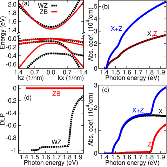
Figures 2(b) and 2(c) show the bulk absorption coefficients for ZB and WZ, respectively, as calculated by equation (10). Although we considered ZB in the [111] unit cell, X- and Z-polarizations have the same absorption as we would expect from the cubic symmetry. One can easily show that the coordinate system rotation we have applied holds this cubic character in the absorption coefficient. Note the shoulder in the curve when the photon energy reaches the SO band energy. For WZ, however, a clear anisotropy between X- and Z-polarizations is found. Before we reach the CH band energy, light is predominantly X-polarized, however, after CH band the Z-polarized absorption increases while X-polarized slightly decreases.
To highlight the polarization differences for ZB and WZ, we show in Fig. 2(d) the DLP, given by equation (16). Since X- and Z-polarizations are the same in ZB, we have a straight line at DLP=0, meaning isotropic absorption. For WZ, the DLP starts at , slightly increases when LH band is reached and after CH band, it rapidly goes to 0 due to the Z-polarization contribution. In the superlattice calculations, we expect that the WZ/ZB mixing and QC effects will change the DLP to some intermediate value between pure ZB and WZ.
III.2 Absorption and PLE measurements
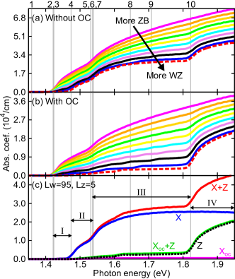
Let us start the superlattice investigation by considering small QC, i.e., relatively large WZ and ZB regions (5-90 nm each with total supercell of 100 nm), values typically found in superlattice samples. Although there is small QC, small regions of WZ and ZB act as perturbations to the bulk states leading to different electronic and optical properties.
In Fig. 3(a) we show the total absorption, , without OC effects. The first (top) solid curve is the case of 90% of ZB and 10% of WZ and we can notice the two characteristic shoulders of the bulk case, the first around transition energy 3 and the second around transition 5. Increasing the mixing of ZB and WZ, new shoulders appear and when we reach the last (bottom) solid curve, 90% of WZ and 10% of ZB, we notice the three characteristic shoulders of WZ bulk case, around transitions 4, 6 and 10, respectively. This WZ characteristic is also noted in the dashed line, which is the 95%WZ/5%ZB. We can also notice from Fig. 3(a) that there is a non-zero absorption coefficient between ZB and WZ energy gaps (transitions 2 and 4) even for large WZ concentrations. This phenomenon is due to the characteristic type-II band alignment of ZB/WZ homojunctions.
When we add OC effects, which are presented in Fig. 3(b), we notice a significant suppression of X-polarization that becomes more evident as WZ/ZB ratio increases. Since in WZ the absorption spectrum in regions I and II mainly comprises sub-bands with a mixture of states , due to HH symmetry, the OC almost forbids the X component from penetrate the NW, therefore the suppression.
The experimental paper of Gadret et al.Gadret et al. (2010) investigates optical properties of InP polytypic superlattices. They report PL and PLE measurements of InP polytypic samples with statistically negligible percentage of ZB. In this regime, they notice 3 absorption edges in the PLE (1.488 eV, 1.532 eV and 1.675 eV) for energies above the PL peak (1.432 eV) and also a long tail at the low energy side of the PL peak. Their system is comparable to our simulation for 100 nm supercell with 95% of WZ and 5% of ZB or even higher WZ percentage over ZB. Indeed, the measured trends are well described by our Fig. 3(c). We can identify 4 regions that we can relate to the experimental spectra: I (between transitions 2/3 and 4, i.e., between ZB and WZ gap energies), II (between transitions 4 and 5/6/7), III (between transitions 5/6/7 and 10) and IV (after transition 10). From the observed data we can assign the three absorption edges to the the beginning of energy regions II, III and IV, respectively. Region I actually comprises the region where the PL peak is observed. Furthermore, the long tail at low energy side of PL can be explained by the type-II confinement of WZ/ZB interface, which has negligible absorption coefficient. Since we are not considering excitons, we do not observe the peaks in the absorption at the band-edge transitions (visible in the experimental data). However, the band-edge character is well described by our model, represented by the shoulders in our graphs. The blue-shift of our band-edge transition energies compared to the experimental data is also related to the lack of excitonic effects in our model.
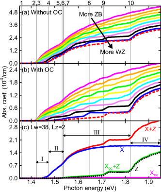
For comparison, we plotted in Fig. 4 the same results but for a 40 nm supercell. In Figs. 4(a) and 4(b) we observe the same trends as before but with more quantization effects, signalled by the extra shoulders or step-like behavior in absorption spectra. As we increase the QC, the number of sub-bands in the same energy range decreases, leading to clear shoulders in the spectra as the photon energy reaches these few sub-bands. In Fig. 4(c), we show the different contribution of X- and Z-polarizations. Comparing to Fig. 3(c), it can be seen that the QC effect is more visible in Z-polarization since this is the confined direction. For the X-polarization, a small red-shift is observed due to greater overlap between states.
III.3 Quantum confinement and crystal phase mixing effects in the DLP
For a better understanding of the optical properties of the InP homojunctions it is valuable to study the DLP. Specifically, we are interested in how polarization properties are modified by different crystal phase mixing and QC.
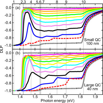
In Fig. 5 we show the behavior of the DLP only under QC effects, no OC included, for the case in which the supercell has 100 nm, Fig. 5(a), and 40 nm, Fig. 5(b). In general, the DLP is very sensitive to ZB insertions: in region I it is close to 0, exception made to systems where WZ regions are largely dominant over ZB ones, about 80%WZ or more for the small QC regime and 70%WZ or more in large QC. For all different WZ/ZB mixing, the limits are bulk WZ and bulk ZB DLP, presented in Fig. 2(d) and showed here with dotted lines.
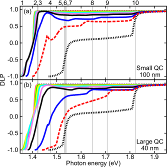
To further analyze the effect of the OC, we present in Fig. 6 the DLP calculations for the same systems previously discussed, including QC and OC effects. Here, we also include OC effects in bulk calculations. In the paper of Mishra et al. Mishra et al. (2007), their PL measurements for pure WZ and ZB NWs with large diameters indicate that for ZB light is strongly polarized along the NW axis, whereas for WZ light is strongly polarized in the perpendicular direction. Our calculations for the bulk case with OC are in very good agreement with these experimental results. In fact, this indicates that OC is a necessary feature to be included in the description. Also, these are the limiting cases for all WZ/ZB mixed systems.
Comparing the results with OC for small QC, Fig. 6(a), and large QC, Fig. 6(b), we also notice that the DLP is very susceptible to ZB concentration, i.e., just a small amount of ZB can switch the DLP from -1 to approximately 1. Moreover, for large QC, WZ features hold more effectively around the gap energy. This happens because WZ holes (parallel to growth direction) have larger effective masses ( and ) and, therefore, are the dominant symmetry to light polarization. Hence, increasing QC can reduce the ZB susceptibility to the DLP.
As a final remark, if we compare our DLP for small QC to the PL spectra measurement of Gadret et al.Gadret et al. (2010), we also notice a non-zero value for parallel polarization. Since their NWs have a statistically negligible percentage of ZB and still present parallel polarization, we believe that this corroborates our results of ZB susceptibility to the DLP.
IV Conclusions
We have expanded our previous polytypic kp modelFaria Junior and Sipahi (2012) to include interband coupling explicitly. The validation of our 88 model was considered for the bulk case and we found how selection rules for WZ and ZB allow different light polarization features.
For the InP polytypic superlattice, we found good agreement between our results and the experimental measurements of PLE and light polarization. Although we have not considered excitonic effects, the energy regions from the paper of Gadret et. al.Gadret et al. (2010) can be mapped to our calculations with small QC and large WZ composition. When QC is increased, step-like features are observed in the interband absorption for Z-polarization, which is parallel to the growth direction.
Since WZ and ZB present different optical selection rules, any mixing of these two crystal phases should combine these different light polarizations. Our DLP calculations for pure ZB or pure WZ are in good agreement with experiments of Mishra et al. Mishra et al. (2007) and OC effects were necessary to match the experimental results. Stronger QC retains WZ behavior of the DLP since WZ HH have larger effective mass than ZB HH. In the polytypic cases, we found that the DLP is very susceptible to ZB regions and only a small amount of ZB drastically increases the DLP. This ZB susceptibility is increased if QC effects are decreased. Furthermore, our results for the DLP also explain the polarized PL measured by Gadret et al.Gadret et al. (2010).
In summary, we believe that our findings provide a theoretical explanation for the optical properties observed in InP polytypic superlattices and also indicate how linear light polarization can be tuned using QC and crystal phase mixing. We wish to emphasize that our theoretical approach is not limited only to InP but also could be applied to other III-V compounds that exhibit polytypismDe and Pryor (2010).
V Acknowledgements
The authors acknowledge financial support from the Brazilian agencies CNPq (grants #138457/2011-5, #246549/2012-2 and #149904/2013-4) and FAPESP (grants #2011/19333-4, #2012/05618-0 and #2013/23393-8). The authors thank James P. Parry and Karie Friedman for kindly proofreading the paper.
Appendix A Second-order corrections
When the interband coupling is considered in kp Hamiltonians, it is necessary to correct some of the second order parameters due to the modification of states that belong to classes A and BLöwdin (1951). For the Luttinger parameters in ZB, we have
| (18) |
and for WZ parameters, we have
| (19) |
Given the corrected Luttinger parameters, we only have to connect them to the ones in the Hamiltonian (2), using the same idea as presented in our previous paperFaria Junior and Sipahi (2012):
| (20) |
For the numerical values presented in Table LABEL:tab:kp_par, we first corrected the ZB parameters and then applied the connection to the polytypic Hamiltonian.
References
- Mohan, Motohisa, and Fukui (2005) P. Mohan, J. Motohisa, and T. Fukui, Nanotechnology 16, 2903 (2005).
- Vu et al. (2013) T. T. T. Vu, T. Zehender, M. A. Verheijen, S. R. Plissard, G. W. G. Immink, J. E. M. Haverkort, and E. P. A. M. Bakkers, Nanotechnology 24, 115705 (2013).
- Pan et al. (2014) D. Pan, M. Fu, X. Yu, X. Wang, L. Zhu, S. Nie, S. Wang, Q. Chen, P. Xiong, S. von Molnár, and J. Zhao, Nano Letters 14, 1214 (2014).
- Lehmann et al. (2013) S. Lehmann, J. Wallentin, D. Jacobsson, K. Deppert, and K. A. Dick, Nano Letters 13, 4099 (2013).
- Khranovskyy et al. (2013) V. Khranovskyy, A. M. Glushenkov, Y. Chen, A. Khalid, H. Zhang, L. Hultman, B. Monemar, and R. Yakimova, Nanotechnology 24, 215202 (2013).
- Ren et al. (2013) F. Ren, K. Wei Ng, K. Li, H. Sun, and C. J. Chang-Hasnain, Applied Physics Letters 102, 012115 (2013).
- Borg et al. (2014) M. Borg, H. Schmid, K. E. Moselund, G. Signorello, L. Gignac, J. Bruley, C. Breslin, P. Das Kanungo, P. Werner, and H. Riel, Nano Letters 14, 1914 (2014).
- Heiss et al. (2014) M. Heiss, E. Russo-Averchi, A. Dalmau-Mallorquí, G. Tütüncüoğlu, F. Matteini, D. Rüffer, S. Conesa-Boj, O. Demichel, E. Alarcon-Lladó, and A. Fontcuberta I Morral, Nanotechnology 25, 014015 (2014).
- Li et al. (2014) K. Li, H. Sun, F. Ren, K. W. Ng, T.-T. D. Tran, R. Chen, and C. J. Chang-Hasnain, Nano Letters 14, 183 (2014).
- Akopian et al. (2010) N. Akopian, G. Patriarche, L. Liu, J.-C. Harmand, and V. Zwiller, Nano Letters 10, 1198 (2010).
- Smit et al. (2014) M. Smit, X. Leijtens, H. Ambrosius, E. Bente, J. van der Tol, B. Smalbrugge, T. de Vries, E.-J. Geluk, J. Bolk, R. van Veldhoven, L. Augustin, P. Thijs, D. D’Agostino, H. Rabbani, K. Lawniczuk, S. Stopinski, S. Tahvili, A. Corradi, E. Kleijn, D. Dzibrou, M. Felicetti, E. Bitincka, V. Moskalenko, J. Zhao, R. Santos, G. Gilardi, W. Yao, K. Williams, P. Stabile, P. Kuindersma, J. Pello, S. Bhat, Y. Jiao, D. Heiss, G. Roelkens, M. Wale, P. Firth, F. Soares, N. Grote, M. Schell, H. Debregeas, M. Achouche, J.-L. Gentner, A. Bakker, T. Korthorst, D. Gallagher, A. Dabbs, A. Melloni, F. Morichetti, D. Melati, A. Wonfor, R. Penty, R. Broeke, B. Musk, and D. Robbins, Semiconductor Science and Technology 29, 083001 (2014).
- Joyce et al. (2013) H. J. Joyce, C. J. Docherty, Q. Gao, H. H. Tan, C. Jagadish, J. Lloyd-Hughes, L. M. Herz, and M. B. Johnston, Nanotechnology 24, 214006 (2013).
- Ponseca et al. (2014) C. S. Ponseca, H. Němec, J. Wallentin, N. Anttu, J. P. Beech, A. Iqbal, M. Borgström, M.-E. Pistol, L. Samuelson, and A. Yartsev, Physical Review B 90, 085405 (2014).
- Murayama and Nakayama (1994) M. Murayama and T. Nakayama, Physical Review B 49, 4710 (1994).
- Ba Hoang et al. (2010) T. Ba Hoang, A. F. Moses, L. Ahtapodov, H. Zhou, D. L. Dheeraj, A. T. J. van Helvoort, B.-O. Fimland, and H. Weman, Nano Letters 10, 2927 (2010).
- Pemasiri et al. (2009) K. Pemasiri, M. Montazeri, R. Gass, L. M. Smith, H. E. Jackson, J. Yarrison-Rice, S. Paiman, Q. Gao, H. H. Tan, C. Jagadish, X. Zhang, and J. Zou, Nano Letters 9, 648 (2009).
- Yong et al. (2013) C. K. Yong, J. Wong-Leung, H. J. Joyce, J. Lloyd-Hughes, Q. Gao, H. H. Tan, C. Jagadish, M. B. Johnston, and L. M. Herz, Nano Letters 13, 4280 (2013).
- Duan et al. (2001) X. Duan, Y. Huang, Y. Cui, J. Wang, and C. M. Lieber, Nature 409, 66 (2001).
- Jiang et al. (2007) X. Jiang, Q. Xiong, S. Nam, F. Qian, Y. Li, and C. M. Lieber, Nano Letters 7, 3214 (2007).
- Wallentin et al. (2012) J. Wallentin, M. Ek, L. R. Wallenberg, L. Samuelson, and M. T. Borgström, Nano Letters 12, 151 (2012).
- Wang et al. (2013) Z. Wang, B. Tian, M. Paladugu, M. Pantouvaki, N. Le Thomas, C. Merckling, W. Guo, J. Dekoster, J. Van Campenhout, P. Absil, and D. Van Thourhout, Nano Letters 13, 5063 (2013).
- Wallentin et al. (2013) J. Wallentin, N. Anttu, D. Asoli, M. Huffman, I. Aberg, M. H. Magnusson, G. Siefer, P. Fuss-Kailuweit, F. Dimroth, B. Witzigmann, H. Q. Xu, L. Samuelson, K. Deppert, and M. T. Borgström, Science 339, 1057 (2013).
- Cui et al. (2013) Y. Cui, J. Wang, S. R. Plissard, A. Cavalli, T. T. T. Vu, R. P. J. van Veldhoven, L. Gao, M. Trainor, M. A. Verheijen, J. E. M. Haverkort, and E. P. A. M. Bakkers, Nano Letters 13, 4113 (2013).
- Akiyama, Nakamura, and Ito (2006) T. Akiyama, K. Nakamura, and T. Ito, Physical Review B 73, 235308 (2006).
- Kitauchi et al. (2010) Y. Kitauchi, Y. Kobayashi, K. Tomioka, S. Hara, K. Hiruma, T. Fukui, and J. Motohisa, Nano Letters 10, 1699 (2010).
- Ikejiri et al. (2011) K. Ikejiri, Y. Kitauchi, K. Tomioka, J. Motohisa, and T. Fukui, Nano Letters 11, 4314 (2011).
- Poole et al. (2012) P. J. Poole, D. Dalacu, X. Wu, J. Lapointe, and K. Mnaymneh, Nanotechnology 23, 385205 (2012).
- Mattila et al. (2006) M. Mattila, T. Hakkarainen, M. Mulot, and H. Lipsanen, Nanotechnology 17, 1580 (2006).
- Mishra et al. (2007) A. Mishra, L. V. Titova, T. B. Hoang, H. E. Jackson, L. M. Smith, J. M. Yarrison-Rice, Y. Kim, H. J. Joyce, Q. Gao, H. H. Tan, and C. Jagadish, Applied Physics Letters 91, 263104 (2007).
- Paiman et al. (2009) S. Paiman, Q. Gao, H. H. Tan, C. Jagadish, K. Pemasiri, M. Montazeri, H. E. Jackson, L. M. Smith, J. M. Yarrison-Rice, X. Zhang, and J. Zou, Nanotechnology 20, 225606 (2009).
- Gadret et al. (2010) E. G. Gadret, G. O. Dias, L. C. O. Dacal, M. M. de Lima, C. V. R. S. Ruffo, F. Iikawa, M. J. S. P. Brasil, T. Chiaramonte, M. a. Cotta, L. H. G. Tizei, D. Ugarte, and A. Cantarero, Physical Review B 82, 125327 (2010).
- Kailuweit et al. (2012) P. Kailuweit, M. Peters, J. Leene, K. Mergenthaler, F. Dimroth, and A. W. Bett, Progress in Photovoltaics: Research and Applications 20, 945 (2012).
- Faria Junior and Sipahi (2012) P. E. Faria Junior and G. M. Sipahi, Journal of Applied Physics 112, 103716 (2012).
- Park and Chuang (2000) S. H. Park and S. L. Chuang, Journal of Applied Physics 87, 353 (2000).
- Löwdin (1951) P. Löwdin, Journal of Chemical Physics 19, 1396 (1951).
- Bastard (1981) G. Bastard, Physical Review B 24, 5693 (1981).
- Baraff and Gershoni (1991) G. Baraff and D. Gershoni, Physical Review B 43, 4011 (1991).
- Chuang (1995) S. L. Chuang, Physics of optoelectronic devices (John Wiley, New York, 1995).
- Ravi Kishore, Partoens, and Peeters (2010) V. V. Ravi Kishore, B. Partoens, and F. M. Peeters, Physical Review B 82, 235425 (2010).
- Califano and Zunger (2004) M. Califano and A. Zunger, Physical Review B 70, 165317 (2004).
- Wang et al. (2001) J. Wang, M. S. Gudiksen, X. Duan, Y. Cui, and C. M. Lieber, Science 293, 1455 (2001).
- Persson and Xu (2004) M. P. Persson and H. Q. Xu, Physical Review B 70, 161310 (2004).
- De and Pryor (2010) A. De and C. E. Pryor, Physical Review B 81, 155210 (2010).
- Chuang and Chang (1996) S. L. Chuang and C. S. Chang, Applied Physics Letters 68, 1657 (1996).