Realization of free-standing silicene using bilayer graphene
Abstract
The available synthesized silicene-like structures have been only realized on metallic substrates which are very different from the standalone buckled silicene, e.g. the Dirac cone of silicene is destroyed due to lattice distortion and the interaction with the substrate. Using graphene bilayer as a scaffold a novel route is proposed to synthesize silicene with electronic properties decoupled from the substrate. The buckled hexagonal arrangement of silicene between the graphene layers is found to be very similar to the theoretically predicted standalone buckled silicene which is only very weakly van der Waals coupled to the graphene layers with a graphite-like interlayer distance of 3.42 Å and without only lattice distortion. We found that these stacked layers are stable well above room temperature.
Introduction. Silicene, a monolayer of hexagonally arranged Si atoms, has attracted a lot of attention in recent years due to its outstanding physical and chemical properties.Takeda ; Roth ; Zhang ; Guzman Due to the similarity of the lattice structures, silicene presents essentially the same electronic properties as graphene.Guzman ; Lebegue ; Cahangirov For example, the band structure of silicene resembles that of graphene with bands crossing linearly at the Fermi level, resulting in a massless Dirac fermion character of the charge carriers. However, unlike graphene, silicene is not stable in a flat configuration: silicon’s larger ionic radius and therefore larger interatomic distances results in a slightly buckled structure with partial sp2 orbitals.Cahangirov ; SahinPRB On the other hand, such buckling creates new possibilities for controlling the band structure of silicene electrically or by functionalizing it with different functional groups.Ni ; Drummond ; Cheng ; Spencer ; Gao ; Quan ; peeters
Since free standing silicene has not been observed in nature and there is no analogue of graphite in the form of stacked layers of silicon, increased efforts have been devoted in recent years to synthesis silicene sheets by implementing more sophisticated methods. A promising approach is to deposit silicon on metallic surfaces (e.g. Ag, Ir, Er, ZrB2). However, this resulted into a plethora of very different crystallographic Si structures depending on the growth conditions and the particular atomic arrangements of the substrate surface.Lalmi2010 ; Lin2012 ; Vogt2012 ; Feng2012 ; Chen2012 ; Jamgotchian2012 ; Chen2013 ; Meng2013 Domain formation, interaction with the substrate and epitaxial strain have turned out to be determining factors that have prevented the observation of typical characteristics of the theoretically predicted free-standing silicene.
In this context, Ag surfaces have been successfully used to grow and synthesize silicene sheets and nanoribbons (see Ref. Kara for review). For example, it was recently demonstrated theoretically WangARXIV that the Dirac cone of silicene when epitaxially grown on Ag (111) is destroyed at the -point and that the experimentally Vogt2012 ; Chen2012 found linear dispersion is coming from the Ag substrate. This conclusion agrees with recent Landau level measurements Lin2013 of silicene on Ag that were supplemented with band structure calculations. The two main reasons for loosing the Dirac cone in silicene are lattice distortions and the strong chemical interaction of silicene with Ag resulting in strongly hybridized states.
Here we present a novel approach where we use graphene layers to gently confine the silicene layer. This approach is expected to result in stable silicene with characteristics that are very close to those predicted for standalone buckled silicene. We show that the silicene Dirac cone is preserved and does not interfere with the graphene Dirac point. The silicene layer is found to be very different from silicene on an Ag substrate Gao_nature and is stable beyond room temperature. Since such structures can naturally arise during epitaxial growth of few-layer graphene on bulk silicon carbide (SiC) by thermal decomposition Berger2006 , our findings can be useful in the understanding of the mechanisms for synthesis of multilayer graphene on SiC.Singh2011 ; Xia2012 ; Wang2012 The results may also initiate further research on graphene-silicene stacked heterostructures with promising structural and electronic properties.
Computational method. In order to investigate the stacked heterostructure, first-principles calculations were performed in the framework of the density functional theory (DFT) within the Perdew-Burke-Ernzerhof (PBE) generalized gradient approximation pbe as implemented in VASP vasp . Corrections due to the van der Waals interactions are introduced using the method of Girmme Grimme . A plane-wave basis set with an energy cutoff of 400 eV was used to expand the valence electronic wave functions while the projector augmented-wave method paw was used to treat the cores. A vacuum layer thinker than 10 Å was used to separate the layers in the supercell which consists of () silicene unit cells between two () graphene unit cells. The lattice mismatch for this configuration is less than 2.5 % based on the separately calculated lattice constants of silicene (3.838 Å) and graphene (2.460 Å). For such a large supercell, momentum space was sampled using a -centered 55 mesh for geometry optimization whereas for calculating the density of states (DOS) a 77 mesh was used. The atomic positions of all atoms were relaxed until the force on each atom reduced to less than 0.02 eV/Å.
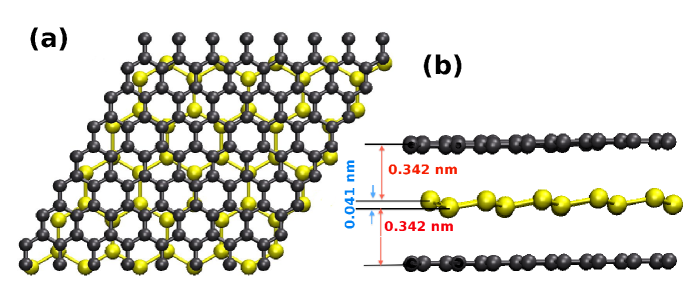
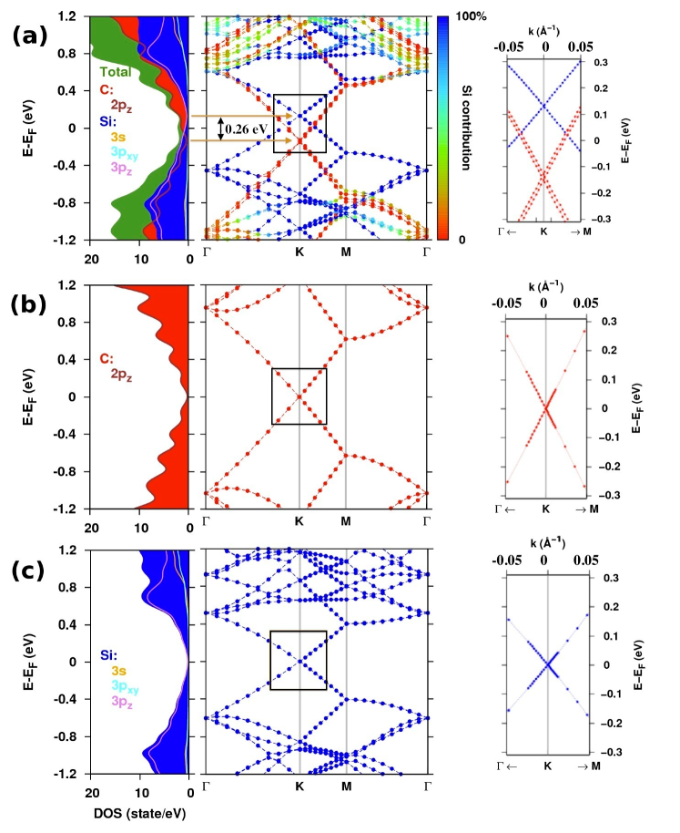
Stacked silicene-graphene. The relaxed structure, depicted in Fig. 1 exhibits a 0.41 Å buckling of the silicene layer and its distance to each of the graphene layers is 3.42 Å. First, we calculate the DOS for this system using a 49-point grid in momentum space and a Gaussian broadening of width 0.1 eV. The DOS projected on the spherical harmonics centered on the atomic positions is then summed up separately over all atoms of the same type to determine the contributions of separate layers. Only the orbitals of the carbon atoms contribute to the DOS in the shown energy interval. The contributions of the , and orbitals of the Si atoms are however vanishing only in the vicinity of the Fermi level. To compare the projected DOS (PDOS) of the stacked system with those of the standalone layers, we show in Figs. 2(b) and (c) the DOS of standalone graphene and silicene. Instead of using primitive cells, we used the same supercell as used for the stacked system, i.e. 55 unit cell for silicene and 88 unit cell for graphene; therefore the absolute values of the DOS’s of the three cases can directly be compared (the DOS of the freestanding graphene is multiplied by a factor of two).
Silicene and graphene both are semimetallic with zero band-gap and vanishing DOS at the Fermi energy. In contrast, the DOS at the Fermi level is no longer zero once the layers are stacked. The minima of the PDOS’s of the silicene and of the graphene layers do not coincide, and therefore their sum never becomes zero resulting in metallic behavior of the stacked system. The minima of PDOS occur at the position of the vertex of the corresponding cone in the band structure plot as indicated by arrows. For the stacked system, the relative contribution of the silicene layer is coded by the color scale, such that a blue (red) point indicates a predominant silicene (graphene) character. It is clearly seen that the the Dirac cones of the layers are coaxial but their vertices do not coincide. The cones corresponding to the two graphene layers are almost degenerate and the distance between their vertices to the vertex of the silicene cone along the energy axis is 0.26 eV. This distance is indeed the same as the difference between the Fermi energies of standalone graphene (-2.455 eV) and silicene (-2.714 eV). When the three layers are stacked, their Fermi levels are shifted with respect to each other so that they become aligned throughout the system. The fact that the distance between the vertices of the cones in the interacting system is the same as the difference of the Fermi energies of the non-interacting free standing layers implies that the electronic structure of the stacked layers is almost not affected by the weak interactions between the layers; the interlayer separation (3.42 Å) is indeed too large to cause rehybridization between the frontier orbitals of the individual layers. Comparing Figs. 2(a), (b) and (c) shows that, apart from a shift of the levels, the overall profile of the DOS and the band structure of the freestanding layers are preserved in the stacked layers, in particular close to the Fermi level. This finding is in contrast to the situation where a silicene layer is put on a metallic substrate, e.g. silicene/Ag where the silicene layer is strongly deformed resulting in a gap opening of about 0.3 eV in the silicene layer WangARXIV . The linear dispersion observed experimentally Vogt2012 ; Chen2012 for this system has been attributed to the metallic substrate rather than the silicene layer.
To gain more informative details, we plot the electronic band structures close to the corner of the Brillouin zone ( point) for the systems in the RHS of Fig. 2. In this region where linear dispersion is seen for all three systems. The slope of the linear fit gives the Fermi velocities as m/s for the silicene branch and m/s for the graphene branches in the stacked system in comparison to those of the freestanding layers i.e. for silicene and m/s for graphene. This confirms the fact that the electronic properties of silicene between double layers of graphene is essentially similar to that of the free standing layers. worth
Notice that several different configurations may be obtained by laterally sliding the layers with respect to each other. However, performing DFT calculations for all possible configurations is infeasible, and therefore we focused only on the one that turned out to be the most stable as determined from molecular dynamics simulations. Since it is unlikely that in any other configuration the interlayer separation becomes less than that of the considered arrangement, one expects that a similar electronic structure is seen for silicene inside graphene layers independent of details of the stacking arrangement.
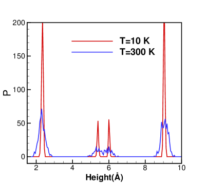
Thermal stability. In order to investigate temperature effects on the structure of our proposed confined silicene, we performed several ab initio molecular dynamics simulations at different temperatures DFTB . We used a large sample containing 1224 atoms for which we were able to observe ripples. The long time molecular dynamics simulations revealed that the silicene layer is stable even beyond 1000 K. The graphene layers have ripples due to temperature induced fluctuations. The average distance between graphene layers at room temperature is almost identical to that at zero temperature, i.e. 0.72 nm. It is interesting to note that the buckled structure of silicene is affected by temperature so that the buckled shape (see Fig. 1(b)) is deformed at room temperature. For instance, the variance of the buckling height i.e. at T=10 K is reduced to 0.033 Å2 when it is confined between the graphene layers as compared to 0.044Å2 for the standalone silicene layer. Figure 3 shows the height distribution for T=10 K and T=300 K. We found that the in-plane hexagonal lattice structure of silicene preserved at room temperature. Surprisingly we found that the lattice constant of silicene is reduced with about 5 and it is almost independent of temperature up to 1000 K while for each graphene layer both the lattice constant and the C-C bond lengths are temperature dependent. The latter is in contrast to the buckling in fluorinated and hydrogenated graphene PRB2013 ; GA , where the buckled structure remains even at T=1000 K without considerable changes in the structures. The reason is that in silicene the buckled structure is not due to pure sp3 hybridization while in fluorinated and hydrogenated graphene the strong sp3 hybridization plays a determining role in its temperature dependence. The important message is that the here proposed silicene layer at room temperature has a buckling height that is random while the two-dimensional nature is reserved.
Conclusions. Using first-principles calculations and ab initio molecular dynamics simulations, we investigated the electronic and structural properties and thermal stability of a silicene layer between bilayer graphene. Such a silicene layer between graphene layers forms a buckled honeycomb structure resembling very closely the properties of standalone silicene. We demonstrated that the electronic and atomic structure of silicene intercalated by graphene layers is almost identical to the one of standalone buckled silicene. Therefore, graphene layers are an almost ideal template for the formation of silicene. This is in contrast with recently synthesized silicene on top of metallic surfaces where hybridization modifies the electronic and structural properties of silicene.
Acknowledgements This work was supported by the Flemish Science Foundation (FWO-Vl) and the Methusalem Foundation of the Flemish Government. M.N.-A was supported by the EU-Marie Curie IIF postdoc Fellowship/299855.
References
- (1) K. Takeda and K. Shiraishi, Phys. Rev. B 50, 14916 (1994).
- (2) U. Röthlisberger, W. Andreoni, and M. Parrinello, Phys. Rev. Lett. 72, 665 (1994).
- (3) Y. Zhang, Y. W Tan, H. L. Stormer, and P. Kim, Nature (London) 438, 201 (2005).
- (4) G. Guzmán-Verri and L. C. Lew Yan Voon, Phys. Rev. B 76, 075131 (2007).
- (5) S. Lebègue and O. Eriksson, Phys. Rev. B 79, 115409 (2009).
- (6) S. Cahangirov, M. Topsakal, E. Aktuerk, H. Şahin, and S. Ciraci, Phys. Rev. Lett. 102, 236804 (2009).
- (7) H. Şahin, S. Cahangirov, M. Topsakal, E. Bekaroglu, E. Akturk, R. T. Senger, and S. Ciraci, Phys. Rev. B 80, 155453 (2009).
- (8) Z. Ni, Q. Liu, K. Tang, J. Zheng, J. Zhou, R. Qin, Z. Gao, D. Yu, and J. Lu, Nano Lett. 12, 113 (2012).
- (9) N. D. Drummond, V. Zólyomi, and V. I. Fal’ko, Phys. Rev. B 85, 075423 (2012).
- (10) Y. C. Cheng, Z. Y. Zhu and U. Schwingenschlögl, Europhys. Lett. 95, 17005 (2011).
- (11) M. J. S. Spencer, T. Morishita, M. Mikami, I. K. Snook, Y. Sugiyama, and H, Nakano, Phys. Chem. Chem. Phys. 13, 15418 (2011).
- (12) N. Gao, W. T. Zheng, and Q. Jiang, Phys. Chem. Chem. Phys. 14, 257 (2012).
- (13) Xin-Quan Wang, Han-Dong Li, and Jian-Tao Wang, Phys. Chem. Chem. Phys. 14, 3031 (2012).
- (14) J. Sivek, H. Sahin, B. Partoens, and F. M. Peeters, Phys. Rev. B 87, 085444 (2013); H. Sahin and F. M. Peeters , Phys. Rev. B 87, 085423 (2013).
- (15) B. Lalmi, H. Oughaddou, H. Enriquez, A. Kara, S. Vizzini, B. Ealet, and B. Aufray, Appl. Phys. Lett. 97, 223109 (2010).
- (16) C.-L. Lin, R. Arafune, K. Kawahara, N. Tsukahara, E. Minamitani, Y. Kim, N. Takagi, and M. Kawai, Appl. Phys. Expr. 5, 045802 (2012).
- (17) P. Vogt, P. De Padova, C. Quaresima, J. Avila, E. Frantzeskakis, M. C. Asensio, A. Resta, B. Ealet, and G. L. Lay, Phys. Rev. Lett. 108, 155501 (2012).
- (18) B. Feng, Z. Ding, S. Meng, Y. Yao, X. He, P. Cheng, L. Chen, and K. Wu, Nano Lett. 12, 3507 (2012).
- (19) L. Chen, C.-C. Liu, B. Feng, X. He, P. Cheng, Z. Ding, S. Meng, Y. Yao, and K. Wu, Phys. Rev. Lett. 109, 056804 (2012).
- (20) H. Jamgotchian, Y. Colignon, N. Hamzaoui, B. Ealet, J. Y. Hoarau, B. Aufray, and J. P. Bibérian, J. Phys.: Condends. Matter 24, 172001 (2012).
- (21) L. Chen, H. Li, B. Feng, Z. Ding, J. Qiu, P. Cheng, K. Wu, and S. Meng, Phys. Rev. Lett. 110, 085504 (2013).
- (22) L. Meng, Y. Wang, L. Zhang, S. Du, R. Wu, L. Li, Y. Zhang, G. Li, H. Zhou, W. A. Hofer, and H.-J. Gao, Nano Lett. 13, 685 (2013).
- (23) A. Kara, H. Enriquez, A. P. Seitsonen, L. C. Lew Yan Voon, S. Vizzini, B. Aufray, and H. Oughaddou, Surface Science Reports 67, 1 (2012).
- (24) Y.-P. Wang and H.-P. Cheng, Phys. Rev. B 87, 245430 (2013).
- (25) C.-L. Lin, R. Arafune, K. Kawahara, M. Kanno, N. Tsukahara, E. Minamitani, Y. Kim, M. Kawai, and N. Takagi, Phys. Rev. Lett. 110, 076801 (2013).
- (26) J. Gao and J. Zhao, Scientific Reports 2, 861 (2012).
- (27) C. Berger, Z. Song, X. Li, X. Wu, N. Brown, C. Naud, D. Mayou, T. Li, J. Hass, A. N. Marchenkov, E. H. Conrad, P. N. First, and W. A. de Heer, Science 312, 1191 (2006).
- (28) V. Singh, D. Joung, L. Zhai, S. Das, S. I. Khondaker, and S. Seal, Progress in Materials Science 56, 1178 (2011).
- (29) C. Xia, S. Watcharinyanon, A. A. Zakharov, R. Yakimova, L. Hultman, L. I. Johansson, and C. Virojanadara, Phys. Rev. B 85, 045418 (2012).
- (30) F. Wang, K. Shepperd, J. Hicks, M. S. Nevius, H. Tinkey, A. Tejeda, A. Taleb-Ibrahimi, F. Bertran, P. Le Fevre, D. B. Torrance, P. N. First, W. A. de Heer, A. A. Zakharov, and E. H. Conrad,
- (31) J. P. Perdew, K. Burke, and M. Ernzerhof, Phys. Rev. Lett., 77, 2865 (1996).
- (32) G. Kresse and J. Hafner, Kresse and J. Hafner, Phys. Rev. B 49, 14251 (1994); G. Kresse and J. Furthmüller, Comp. Mater. Sci. 6, 15 (1996); G. Kresse and J. Furthmüller, Phys. Rev. B 54, 11169 (1996).
- (33) S. Grimme, J. Comp. Chem. 27, 1787 (2006).
- (34) P. E. Blöchl, Phys. Rev. B 50, 17953 (1994); G. Kresse and D. Joubert, Phys. Rev. B 59, 1758 (1999).
- (35) It is worth noting that when the supercell is composed of or (or in general , where is an integer) primitive cells, then the corners of the Brillouin zone are unfolded back again on to the corners of the first Brillouin zone of the primitive cell, i.e. the points. Therefore, the Dirac cones of silicene and graphene layers are coaxial in our case. However, since their vertices are shifted along the common axis, their intersection (i.e. the region of linear dispersion) is away from the K-point by Å-1, as seen in the band structure plot enlarged around the point in Fig. 2
- (36) For the molecular dynamics simulations we used the density functional-based tight-binding approach; see ,e.g., D. Porezag, T. Frauenheim, T. Kohler, G. Seifert, and R. Kaschner, Phys. Rev. B 51, 12947 (1995). This enables us to perform simulations for large supercells. We used the implemention in the DFTB+ code presented in B. Aradi, B. Hourahine, and Th. Frauenheim, J. Phys. Chem. A, 111, 5678 (2007). Parameters are taken from E. Rauls, R. Gutierrez, J. Elsner, and Th. Frauenheim, Sol. State Comm. 111, 459 (1999).
- (37) S. K Singh, S. Goverapet Srinivasan, M. Neek-Amal, S. Costamagna, Adri C. T. van Duin, and F. M. Peeters, Phys. Rev. B 87, 104114 (2013).
- (38) S. Costamagna, M. Neek-Amal, J. H. Los, and F. M. Peeters, Phys. Rev. B 86, 041408 (2012).