Two-dimensional disorder for broadband, omnidirectional and polarization-insensitive absorption.
Matteo Burresi1,2,∗, Filippo Pratesi1, Kevin Vynck1,∗∗, Mauro Prasciolu3, Massimo Tormen4, Diederik S. Wiersma1,2
1,European Laboratory for Non-linear Spectroscopy (LENS), Via N. Carrara, 1. I-50019 Sesto Fiorentino, Firenze, Italy.
2Istituto Nazionale di Ottica (CNR-INO), Largo Fermi 6, 50125 Firenze, Italy.
3 IOM-CNR, Laboratorio TASC, S.S. 14 Km 163.5, 34149 Trieste, Italy.
4 Laboratorio Nazionale TASC-INFM, Basovizza, I-34012 Trieste, Italy.
present/current address: Institut Langevin, ESPCI ParisTech, 1 rue Jussieu, 75005 Paris, France. ∗burresi@lens.unifi.it
Abstract
The surface of thin-film solar cells can be tailored with photonic nanostructures to allow light trapping in the absorbing medium. This in turn increases the optical thickness of the film and thus enhances their absorption. Such a coherent light trapping is generally accomplished with deterministic photonic architectures. Here, we experimentally explore the use of a different nanostructure, a disordered one, for this purpose. We show that the disorder-induced modes in the film allow improvements in the absorption over a broad range of frequencies and impinging angles.
OCIS codes: (000.0000) General.
References and links
- [1]
- [2] R. D. Schaller, M. Sykora, J. M. Pietryga, and V. I. Klimov, “Seven excitons at a cost of one: redefining the limits for conversion efficiency of photons into charge carriers,” Nano Letters 6, 424–429 (2006).
- [3] J. M. Zahler, K. Tanabe, C. Ladous, T. Pinnington, F. D. Newman, and H. A. Atwater, “High efficiency InGaAs solar cells on si by InP layer transfer,” Applied Physics Letters 91, 012108–012111 (2007).
- [4] C. G. Granqvist, “Transparent conductors as solar energy materials: A panoramic review,” Solar energy materials and solar cells 91, 1529–1598 (2007).
- [5] G. Brown and J. Wu, “Third generation photovoltaics,” Laser & Photonics Review 3, 394–405 (2009).
- [6] H. Chen, J. Hou, S. Zhang, Y. Liang, G. Yang, Y. Yang, L. Yu, Y. Wu, and G. Li, “Polymer solar cells with enhanced open-circuit voltage and efficiency,” Nature Photonics 3, 649–653 (2009).
- [7] F. C. Krebs, “Fabrication and processing of polymer solar cells: a review of printing and coating techniques,” Solar Energy Materials and Solar Cells 93, 394–412 (2009).
- [8] V. M. Andreev, V. A. Grilikhes, V. P. Khvostikov, O. A. Khvostikova, V. D. Rumyantsev, N. A. Sadchikov, and M. Z. Shvarts, “Concentrator PV modules and solar cells for TPV systems,” Solar energy materials and solar cells 84, 3–17 (2004).
- [9] P. Spinelli, M. Verschuuren, and A. Polman, “Broadband omnidirectional antireflection coating based on subwavelength surface mie resonators,” Nature Communications 3, 692 (2012).
- [10] Y. Park, E. Drouard, O. E. Daif, X. Letartre, P. Viktorovitch, A. Fave, A. Kaminski, M. Lemiti, and C. Seassal, “Absorption enhancement using photonic crystals for silicon thin film solar cells,” Optics Express 17, 14312–14321 (2009).
- [11] S. E. Han and G. Chen, “Optical absorption enhancement in silicon nanohole arrays for solar photovoltaics,” Nano Letters 10, 1012–1015 (2010).
- [12] H. A. Atwater and A. Polman, “Plasmonics for improved photovoltaic devices,” Nature Materials 9, 205–213 (2010).
- [13] V. E. Ferry, M. A. Verschuuren, M. C. van Lare, R. E. I. Schropp, H. A. Atwater, and A. Polman, “Optimized spatial correlations for broadband light trapping nanopatterns in high efficiency ultrathin film a-si:h solar cells,” Nano Letters 11, 4239–4245 (2011).
- [14] X. Meng, G. Gomard, O. El Daif, E. Drouard, R. Orobtchouk, A. Kaminski, A. Fave, M. Lemiti, A. Abramov, P. Roca i Cabarrocas, and C. Seassal, “Absorbing photonic crystals for silicon thin-film solar cells: Design, fabrication and experimental investigation,” Solar Energy Materials and Solar Cells 95, Supplement 1, S32–S38 (2011).
- [15] S. B. Mallick, M. Agrawal, A. Wangperawong, E. S. Barnard, K. K. Singh, R. J. Visser, M. L. Brongersma, and P. Peumans, “Ultrathin crystalline-silicon solar cells with embedded photonic crystals,” Applied Physics Letters 100, 053113 (2012).
- [16] Z. Yu, A. Raman, and S. Fan, “Fundamental limit of nanophotonic light trapping in solar cells,” Proceedings of the National Academy of Sciences 107, 17491–17496 (2010).
- [17] D. M. Callahan, J. N. Munday, and H. A. Atwater, “Solar cell light trapping beyond the ray optic limit,” Nano Letters 12, 214–218 (2012).
- [18] A. Bozzola, M. Liscidini, and L. C. Andreani, “Photonic light-trapping versus lambertian limits in thin film silicon solar cells with 1d and 2d periodic patterns,” Optics Express 20, A224–A244 (2012).
- [19] K. Kempa, M. J. Naughton, Z. F. Ren, A. Herczynski, T. Kirkpatrick, J. Rybczynski, and Y. Gao, “Hot electron effect in nanoscopically thin photovoltaic junctions,” Applied Physics Letters 95, 233121 (2009).
- [20] C. Rockstuhl, S. Fahr, K. Bittkau, T. Beckers, R. Carius, F.-J. Haug, T. Söderström, C. Ballif, and F. Lederer, “Comparison and optimization of randomly textured surfaces in thin-film solar cells,” Optics Express 18, A335–A341 (2010).
- [21] E. R. Martins, J. Li, Y. Liu, J. Zhou, and T. F. Krauss, “Engineering gratings for light trapping in photovoltaics: The supercell concept,” Physical Review B 86, 041404 (2012).
- [22] A. Oskooi, P. A. Favuzzi, Y. Tanaka, H. Shigeta, Y. Kawakami, and S. Noda, “Partially disordered photonic-crystal thin films for enhanced and robust photovoltaics,” Applied Physics Letters 100, 181110–181114 (2012).
- [23] P. Kowalczewski, M. Liscidini, and L. C. Andreani, “Engineering gaussian disorder at rough interfaces for light trapping in thin-film solar cells,” Optics Letters 37, 4868–4870 (2012).
- [24] M. M. Sigalas, C. M. Soukoulis, C.-T. Chan, and D. Turner, “Localization of electromagnetic waves in two-dimensional disordered systems,” Physical Review B 53, 8340–8348 (1996).
- [25] C. Vanneste and P. Sebbah, “Complexity of two-dimensional quasimodes at the transition from weak scattering to anderson localization,” Physical Review A 79, 041802 (2009).
- [26] F. Riboli, P. Barthelemy, S. Vignolini, F. Intonti, A. D. Rossi, S. Combrie, and D. S. Wiersma, “Anderson localization of near-visible light in two dimensions,” Optics Letters 36, 127–129 (2011).
- [27] K. Vynck, M. Burresi, F. Riboli, and D. S. Wiersma, “Photon management in two-dimensional disordered media,” Nature Materials 11, 1017–1022 (2012).
- [28] A. F. Oskooi, D. Roundy, M. Ibanescu, P. Bermel, J. D. Joannopoulos, and S. G. Johnson, “Meep: A flexible free-software package for electromagnetic simulations by the fdtd method,” Computer Physics Communications 181, 687–702 (2010).
- [29] R. A. Street, Hydrogenated Amorphous Silicon (Cambridge University Press, 2005).
- [30] Z. Yu, A. Raman, and S. Fan, “Thermodynamic upper bound on broadband light coupling with photonic structures,” Physical Review Letters 109, 173901 (2012).
1 Introduction.
The quest for efficient harvesting of solar radiation is one of the major areas of research in the renewable energy field, characterized by an interdisciplinary character, ranging from material science [2, 3, 4, 5, 6, 7] to optics [8, 9] and nanophotonics [10, 11, 12, 13, 14, 15]. In particular, the nanophotonic community has been producing a great deal of alternative strategies to improve the performance of the various photovoltaic technologies. Among the third-generation solar cells, the thin-film technologies are the most promising alternative to the commercially available one, made out of different, sometimes very expensive and rare, materials (e.g., CdTe, CIGS)[5]. Due to the reduced thickness of these thin films (even below 1 m), nanophotonics is particularly suited for improving the solar cell absorption [16, 17, 18]. Through different photonic architectures it is possible to augment the optical absorption by trapping light within thin and ultra-thin films, the latter being desirable to decrease costs and efficiently extract the photo-generated charge carriers [19]. So far, nanophotonics has been aiming at increasing the absorption by patterning deterministic nanostructures (periodic or even quasi-periodic) on the film, giving rise to partially guided modes [14, 18] in which also the photon density of states can be manipulated for absorption enhancement purposes [17]. A rising interest in alternative strategies based on non-deterministic nanostructures has been developing [20, 21, 22, 23]. Recently, a properly engineered random patterning which gives rise to 2D disorder modes on the verge of light (Anderson) localization [24, 25, 26] has been proposed as light trapping scheme [27]. The impinging light can easily couple in the 2D random structure increasing the absorption of the film over a remarkably broad range of frequencies and angle of incidence [27]. Given the random nature of these architectures, the optical properties of it are expected to be less susceptible to imperfections, suggesting the possibility to envision cheaper fabrication methodologies.
In this work, we present a proof-of-principle investigation of the absorption enhancement induced by a 2D disordered photonic architecture applied to a thin film material. We find that this strategy improves the absorption of thin films over an extremely large frequency bandwidth, independently of the angle of incidence and light polarization. This work provides experimental evidence that the use of deterministic structures is not the only route for nanophotonic applications in photovoltaics but rather the introduction of random photonic architectures can provide efficient light absorption at any angle of incidence.
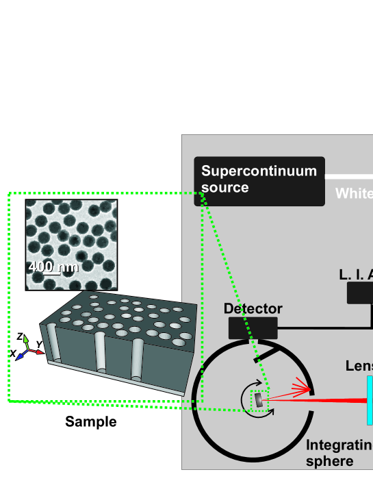
2 Sample and experimental setup
We investigate a sample made of a layer of amorphous silicon (a-Si) of thickness nm, deposited on top of 100 nm of silver. An adhesion layer of chromium (5 nm) is placed between a-Si and Ag (Supplementary Data). A random distribution (obtained with a Random Sequential Addition algorithm, as in [27]) of holes is patterned over an area of 300 m by 300 m with electron beam lithography and plasma etching processes. The hole diameter is 270 nm and they fully perforate the a-Si film (full-etched sample). The hole size has been roughly chosen to be comparable to the wavelength of light in the medium in order to have a significant scattering strength. However, the optimization of this parameter does not require particular attention since the Mie resonance of a two dimensional air cylinder in a silicon environment has a very broad frequency response. This aspect contribute to the optical robustness of the disorder nanophotonic architecture, which does not demand for a high quality monodispersity of the holes. The inset in Figure 1 shows an electron micrograph image of the sample and a 3D schematics of it. In order to verify the absorption enhancement not only over a broad spectral range but also for all angles of incidence and polarizations, an accurate optical setup for calibrated absorption measurements has been constructed (Figure 1). The probing white light is emitted by a commercial supercontinuum source (SM-8-OEM, provided by Leukos SAS). The laser intensity has been monitored wavelength-by-wavelength to compensate for any possible spectral drift or power fluctuation of the laser. As depicted in Figure 1, with the use of a monochromator we select the probing wavelength before light impinges on the sample. We insert an optical long pass filter (nm) to get rid of the higher diffractive orders of the grating of the monochromator. A polarizer selects the impinging light polarization and a beam sampler is used to pick up part of the light at a specific wavelength to monitor the intensity. The probing light is mildly focused on the random pad with an achromatic doublet (working distance 200 mm) to reduce the chromatic aberration and ensure that the focal spot is fully enclosed in the random pad. To perform measurements as a function of angle we mount the sample on a rotation stage. Given the presence of the Ag substrate, the transmission of the sample vanishes and thus only reflection () measurements are required to obtain the absorption . More accurately, the reflection is constituted by two components, namely the directly (ballistic) reflected light () and the scattered light (). To measure exactly , the spectrum of the total reflection must be detected and thus the sample is inserted in an integrating sphere, as shown in Figure 1. Also, the sample is tilted by 4 degrees to prevent the directly reflected light to escape the integrating sphere. For the reference measurements a silver mirror mounted on an identical mount has been used to reproduce exactly the experimental conditions. A silicon large area detector is placed at the surface of the integrating sphere. Both signals are acquired with a lock-in detection scheme.
3 Spectroscopic absorption measurements.
We compare the absorption spectrum thus retrieved for the random pad with the one for a bare slab of the same thickness, as shown in Figure 2a. Also, the absorption that the bare slab would have if a perfect antireflection coating (PAR) was present is shown in green (single-pass absorption). Such a graph has been retrieved by applying the Lambert-Beer law (neglecting reflectance at the film/air interface) and by measuring the dispersion of the material with ellipsometry. We investigate the spectral region (between 650 nm and 1000 nm) where we expect to have the largest benefit from the coherent light trapping scheme we propose, since the absorption drops quickly as a function of wavelengths (see Figure 2). In this range of wavelengths the absorption length of a-Si varies approximately from 100 nm to 4 m, which corresponds to and , respectively.
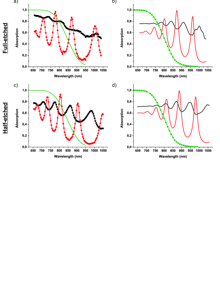
In the case of the bare slab the Fabry-Perot fringes are visible, yielding to small frequency windows in the near-infrared where the absorption is significantly higher than in the case of the PAR. Due to the optical impedance mismatch at the air/a-Si interface the absorption performance of the bare slab at shorter wavelength is far from the PAR case, despite the absorption length of a-Si is much smaller than the thickness of the slab. In contrast, the absorption of the random pad at these wavelengths is close to the PAR case and outperforms both the ideal and the bare slab case for long wavelengths.
Depending on the absorption length of the bulk material, we can find different explanations for the absorption enhancement. In particular, as it has been shown in Ref. [27], for a sufficiently weak absorbtion (long wavelengths regime) the in-plane multiple scattering and interference effects dictate transport in the structured film. These give rise to quasi-guided modes in the random pad through which a relevant absorption enhancement can be achieved.
As sanity check, 3D Finite Difference Time Domain (FDTD) calculations have been performed using a freely available software package [28], by considering the dispersion of the film obtained by ellipsometry up to 950 nm of wavelength (see Figure 2b) and a perfect metal instead of the metal substrate. A good qualitative agreement with the experimental results is found. Quantitatively, however, the calculated and measured absorption slightly differs111The small difference in the frequency of the resonances between experiment and calculation is mostly given by the difficulties to implement an the actual dispersion of the material in the software and the experimental uncertainty on the thickness of the film.. It must be pointed out that two important physical mechanisms are not taken into account by the calculations: i) the excitation of Surface Plasmon Polaritons (SPPs) induced by the holes close to the Ag surface and ii) the presence of dangling bonds [29] for a-Si in the holes surfaces. Both phenomena can lead to an increase of the absorption of the real system, due to the metal absorption and to the absorption from defect states, respectively. In order to understand their influence, a different kind of random pad is fabricated in which the holes are 240 nm shallower than the slab thickness (half-etched system). Given the distance of the bottom of the holes to the metal substrate, the excitation of SPPs is drastically reduced, if not suppressed. In Figure 2c and d measured and calculated absorption spectra, respectively, are shown for the half-etched system. The quantitative deviations between the theoretical expectations and experiment is clearly reduced. This seems to suggest that the SPPs where mostly responsible for the quantitative discrepancy between theory and experiment (Figure 2a and b) and that the presence of dangling bonds has a minor contribution on the enhancement of optical absorption. For the sake of completeness, it must be pointed out that only photocurrent generation experiments could definitely prove the above statement. However, such a measurement goes beyond the scope of this work, which aims only to show that with this novel random nanophotonic architecture a remarkable absorption enhancement can be achieved. Despite the fact that the absorption of the random pad does not show evident spectral features, the enhanced absorption undergoes different regimes. The absorption mechanism can be better investigated by studying the backscattered light (). is measured rotating the sample such that the probing beam impinges normally to the surface and the directly reflected light () escapes from the integrating sphere. In Figure 3a is shown the measured and , whereas the direct reflection is retrieved as the difference between the two. At short wavelengths the reflection of the random pad is mostly given by , due to the refractive index contrast at the air/a-Si interface. Since at these wavelengths is only few percents, we infer that, when light enters the film, it is absorbed. Indeed the absorption length of the bulk a-Si for wavelengths between 650 nm to 750 nm is of the order of nm and thus much shorter than the thickness of the slab and comparable to the distance between holes. As a result, light is absorbed long before the in-plane multiple scattering is performed and thus no photonic mode participates to the increase of the absorption. Thus, the observed enhancement at short wavelengths is mostly due to the smaller refractive index contrast at the random pad/air interface with respect to the bare slab/air one. As a matter of fact, the introduction of holes in the thin film act as a ’natural’ anti-reflection coating which reduces the backreflection of light.
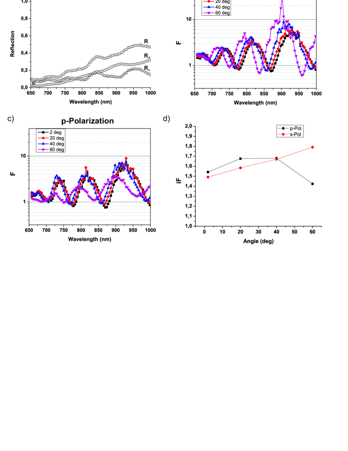
In contrast, at long wavelengths the pronounced increase of absorption can be explained by coupling to the in-plane disorder modes. At these wavelengths, the absorption of the randomly structured film is as large as the absorption of an analogous film in the single-pass regime but 10 times thicker. The diffused reflection at longer wavelength, which is around 10%, is mostly due to light which undergoes single scattering events without coupling to the slab and then, after reflection by the metal substrate, propagates through the silicon film. Since the absorption decreases at long wavelengths, is expected to increase at long wavelengths.
4 Angular response of the photonic architecture
For photovoltaic applications, angular and polarization characterizations are of crucial importance, since the solar radiation can impinge on a photovoltaic cell under different angles with random polarizations.
In order to show the performance of a photonic architecture, the absorption enhancement is the most used figure of merit by the nanophotonic community [16, 17]. It has been shown that the absorption enhancement achieved by nanophotonic architectures can have extremely high values (up to ) in weakly absorbing materials, in particular when the reference is the single-pass absorption (green curves in Figure 2) [16]. Here we define the spectral absorption enhancement which compares the spectral absorption of the nanostructured film with respect to the spectral absorption of the bare slab . We performed measurements rotating the sample such that the angle of incidence varies from 4 to 60 degrees, for both slab and random pads. Figure 3b and c show as a function of angle for two orthogonal polarizations (s and p, respectively). Given the pronounced Fabry-Perot oscillations, frequency windows where the absorption enhancement is as high as 10 times are visible, with a clear improving trend towards long wavelengths, where the absorption length of the material is longer.
The overall trend of as a function of angle and wavelengths can be better seen by calculating the integrated weighted with the air-mass coefficient 1.5 spectrum for the incident light. is defined as , where, in our case, nm and nm. Figure 3d shows as a function of incident angle for the two polarizations. As expected both polarizations exhibit a similar at small angles. Please note that given the significant absorption of the material with respect to its thickness, the architecture cannot achieve orders of magnitude of absorption enhancement [30]. Quantitatively, the response as a function of angle is similar for both polarizations, as expected given the random nature of the nanostructures, but a clear difference trend can be seen. In particular for the p-polarization slightly decreases at large angles. As the angle of incidence approaches the Brewster’s angle, the p-polarization experiences a smaller reflectance which in turn increases the absorption of the film. Experimentally we verified that the absorption of the bare slab increases faster than nanostructured case as a function of angles, yielding a decrease of .
5 Conclusions
In conclusion, we experimentally verified that the presence of in-plane disorder modes in a thin film can be used to significantly enhance the light absorption of commercially available thin-film solar cells. Such an increase of absorption occurs on a broad frequency bandwidth and angular range (up to 60 degrees of incident angle). On one hand, at long wavelengths we obtained an increase of the absorption due to the light coupling to the modes arising from the in-plane multiple scattering and interference effects. On the other hand, at shorter wavelengths the absorption enhancement is given by the lower effective refractive index induced by the nanopatterning, which acts as a broadband antireflection coating embedded in the film itself. In this wavelength regime the very short absorption length does not allow the guided modes formation by multiple scattering. We believe that the omnidirectionality of the absorption enhancement for all polarizations makes this disorder photonic strategy particularly promising for thin-film photovoltaic applications. This work experimentally proves that deterministic structures are not the only possible way towards an improvement of thin-film absorption by nanophotonic means.
Acknowledgement
We wish to thank F. Riboli and G. Conley for fruitful discussions. This work is supported by the European Network of Excellence Nanophotonics for Energy Efficiency, CNR-EFOR, and ENI S.p.A. Novara.