Ballistic transport at room temperature in micrometer size multigraphene
Abstract
The intrinsic values of the carriers mobility and density of the graphene layers inside graphite, the well known structure built on these layers in the Bernal stacking configuration, are not well known mainly because most of the research was done in rather bulk samples where lattice defects hide their intrinsic values. By measuring the electrical resistance through microfabricated constrictions in micrometer small graphite flakes of a few tens of nanometers thickness we studied the ballistic behavior of the carriers. We found that the carriers’ mean free path is micrometer large with a mobility cm2/Vs and a carrier density cm-2 per graphene layer at room temperature. These distinctive transport and ballistic properties have important implications for understanding the values obtained in single graphene and in graphite as well as for implementing this last in nanoelectronic devices.
pacs:
72.15.Lh, 72.80.Cw, 73.23.Ad, 81.05.UwThe existence of massless-like quasiparticles (Dirac fermions) found in the quasi-two dimensional graphite structure Luk’yanchuk and Kopelevich (2004); Li and Andrei (2007); Orlita et al. (2008) and in single graphene layers Novoselov et al. (2005); Zhang et al. (2005) enhanced enormously the interest in these materials, implying not only the start of a qualitative new physicsNeto et al. (2009) but also the possibility of nanotechnological improvements Geim (2009); Ouyang et al. (2010). The search for highest carrier mobility together with lowest carrier density in graphene remains a main research issue of this two-dimensional model system also because of their implications in future applications in nanoelectronics. It is nowadays known, however, that graphene properties can be sensitively affected by the environment, particularly by the substrate Sabio et al. (2008); García et al. (2010) and by disorder Morozov et al. (2008). This fact is supported by experiments done on suspended graphene layers where mobility approaching cm2/Vs at carrier densities cm-2 at K has been reached Du et al. (2008); Bolotin et al. (2008). Nevertheless, the expectations on the use of single graphene layer (SGL) on substrates are high Geim (2009) and in spite of the detrimental substrate influence, SGL exhibits ballistic transport in the 100 nm range at room temperature Lin et al. (2009) and in the m range at very low temperatures Miao et al. (2007).
By measuring the resistance and its ballistic characteristics we studied the transport behavior of the carriers of the graphene layers inside the graphite structure. This study allows us to obtain the carriers’ values for the mean free path, carrier density and mobility. Due to the natural packing of the graphene layers inside graphite we expect not only a natural shielding from the environmental influence but their should be actually more ideal than SGL standing alone or on a substrate. Although some experiments have been done in graphene bilayers, the actual intrinsic values of these transport parameters for the graphite structure remain still not well known simply because their are very sensitive to lattice defects Arndt et al. (2009), grain boundaries González et al. (2007); García et al. (2008) and internal interfaces Barzola-Quiquia et al. (2008), which in general trigger high carrier density with low mobility. Recent results obtained on bulk oriented pyrolytic graphite samples indicate ballistic transport in the micrometer range at K with a very low carrier density cm-2 and huge mobility cm2/Vs García et al. (2008).
The graphite flakes we report here were obtained by exfoliation of a highly oriented pyrolytic graphite sample of ZYA grade. Using an ultrasonic technique we obtained several flakes that we selected by measuring the resistance, its temperature dependence and micro-Raman signals and taking into account the overall shape and dimension of the sample, its surface and thickness. The Au contacts for longitudinal resistance measurements were prepared using electron beam lithography, see Fig. 1.
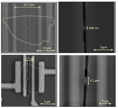
The measurement of the carrier mean free path is not straightforward and in general the value obtained depends on several others, not well known parameters within the selected transport model, usually based on a Drude-Boltzmann approach. However, in case of ballistic conduction there is a transparent method to obtain without adjustable parameters, successfully used for macroscopic graphite samples as described in García et al. (2008). The method is based on the measurement of the longitudinal resistance as a function of the geometry of a constriction located between the voltage electrodes (see Fig. 1). We prepared these constrictions with the focused ion beam of a dual beam microscope. We avoided the modification of the crystalline structure of the samples due to the ion beam spread by protecting them with a negative electron beam resist (AR-N 7500) of nm thickness, a method successfully tested in graphite and described in Barzola-Quiquia et al. (2010).
As shown in García et al. (2008) the resistance of a graphite sample of width , thickness , with a constriction of size and length connecting two half-parts of resistivity is given by:
| (1) |
At the rhs of Eq.(1) the first term corresponds to the ballistic Knudsen-Sharvin resistance García et al. (2008); the second, logarithmic term to the ohmic, spreading resistance in two-dimensions with the smooth function for Wexler (1966). The last term is due to the ohmic resistance of the constriction tube itself. The constant takes care of the influence of the sample shape, the topology and the location of the electrodes in the sample. It is equal to 1 for the geometry used in sample A where the voltage electrodes are deposited through the whole sample width and their distance is . This can be verified from the measurement of the resistance as a function of , as it is shown below. To keep the third term, the ohmic contribution of the constriction, small enough we prepared constrictions with length m. The results presented here correspond to two samples, sample A and B with different geometry and resistivity. Sample A (B) had a size (distance between voltage electrodes width thickness) of m3 (m3) and a resistivity K)cm (cm), see Fig. 1.
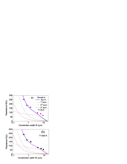
The simplest and direct way to check the ballistic contribution and obtain the mean free path (without further adjustable parameter) is just measuring the resistance as a function of the constriction width in combination with Eq. (1). The results for sample A at two temperatures are shown in Fig. 2. In that figure one recognizes that for m the ballistic contribution overwhelms the ohmic ones, see Eq.(1), indicating that the mean free path should be of this order. The theoretical lines in Fig. 2 were obtained using m and m at 60 K and 250 K, respectively. We estimate an error of for these values determined by the errors in the measurement of the sample and constriction geometry. We can calculate now the Fermi wavelength per graphene layer using the relation
| (2) |
with the number of graphene layers in the sample. For sample A we obtain then m at 250 K (60 K).
In case is larger than the constriction size, the ballistic contribution to the resistivity is better described by the inverse of a sum of an energy - and transverse wave vectors -dependent transmission probabilities , where Stauber et al. (2007). The maximum possible is determined by the constriction width , decreasing the smaller . In this case the increase in resistance is expected to show an oscillatory behavior as a function of or García and Escapa (1989); Snyman et al. (2008) as observed experimentally in Bismuth (Bi) nanowires Costa-Krämer et al. (1997) as well as in GaAs devices van Wees et al. (1988); Wharam et al. (1988).
Note that the distance between voltage electrodes in sample A is larger than the obtained . The larger the sample the larger is the probability to have defective regions with larger carrier concentration and smaller mean free path within the voltage electrodes Arndt et al. (2009). Therefore we repeated the experiment with sample B that shows lower resistivity and with a smaller voltage electrode distance, see Fig. 1. Figure 3 shows the measured resistance normalized by its value at a constriction m; in this way we pay attention to the huge relative increase decreasing and we need neither the absolute value of nor of to compare the data with theory.
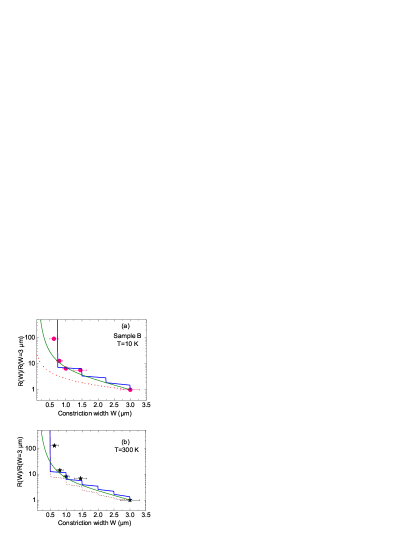
In Fig. 3 one realizes that for sample B Eq. (1) does not describe the experimental data even assuming the largest possible mean free path equal to the voltage electrode distance of m. The data can be reasonably well fitted dividing the ballistic term in Eq. (1) by the function , which generates steps whenever the constriction width with an integer. From the fits we obtain the parameters m and m at 300 (10) K, see Fig. 3. Using other values of , for example m, see Fig. 3, the function does not fit the data indicating indeed that the carriers behave ballistically between the voltage electrodes, leaving actually the only free parameter.
The ballistic analytical function we use resembles the theoretical results with similar steps obtained in Snyman et al. (2008) where the conductance vs. was calculated numerically for a SLG with an electrostatically potential landscape that resembles a constriction. An analytical average value or envelope of this stepped function is obtained replacing the truncation function by , see Fig. 3. This exponential function represents the impossibility of an electron to propagate in the constriction when , as also occurs for the propagation of light in a tube.
The data appear to be better fitted by the stepped function than with the exponential one. The important result obtained for sample B is the huge increase of the resistance for m indicating clearly a larger . The larger in sample B to the one obtained in sample A is compatible with the measured resistivity difference.
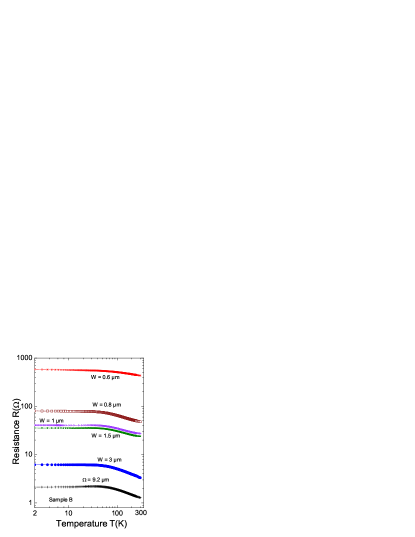
As a further proof that the huge increase of the resistance decreasing the constriction width in sample B is due to the ballistic contribution and not due to, e.g. a possible disorder produced by the ion beam on the graphite structure, we show in Fig. 4 the temperature dependence of the measured resistance without and with the different constriction widths. We observe that in spite of the huge resistance increase the temperature dependence remains similar. The small differences in the temperature dependence of the resistance, decreasing slightly more at K at large values of than at the smallest , e.g. (sample without constrictions) to for m (see Fig. 4) can be explained taking into account that the ballistic contribution (first term in the r.h.s of Eq.(1)) is weakly dependent. At low values of the ohmic contributions start to be negligible compared with the ballistic one (see Fig. 2) and therefore the temperature dependence of slightly reduces decreasing , see Fig. 4.
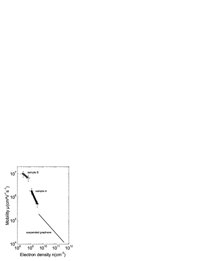
As shown in García et al. (2008) the temperature dependence of can be used now to obtain and the mobility per graphene layer, this last given by . Since the density of carriers per graphene layer can be calculated from we show in Fig. 5 the mobility vs. carrier density for the two samples and compare them with data from literature for suspended SLG. From these results we clearly recognize the much larger mobility and smaller density of carrier for the thin graphite flakes, supporting the view that the graphene layers within graphite are of better quality than SLG and with a smaller carrier density. Obviously sample B is not free from defects and therefore we expect that the obtained values might still be improved in ideal, defect free graphite structures.
The rather weak temperature dependence of (or ) obtained for the here reported samples is a non-trivial result that deserves a comment. For the simple case of a linear dispersion relation we expect that the and therefore or for a quadratic dispersion relation. The data obtained indicate that the carrier density increases at most a factor of ten between 10 K and 300 K. We may speculate the reason for this behavior, either by comparing our results with those found in Bi and a possible band splitting or the existence of an intrinsic energy gap in graphite.
Firstly, we note that both materials, graphite and Bi, have very small carrier densities with small anisotropic effective carrier mass. For a long time it was unclear why there was such a difference in the carriers’ mean free path between the two structures. While the carriers in Bi show Km,Brown (1970); Yang et al. (2000) the values reported for graphite in literature are more than one order of magnitude smaller at the same temperature. The results of this work finally put an end to this apparent difference showing that also in graphite the carriers’ mean free path can be micrometer large with a low carrier density.
The large of the order of the sample dimensions may affect the band structure. For m, and for the typical sample dimensions we report here only the first five quantized wave vectors in reciprocal space are occupied (meV) indicating that the usual continuous approximation of the band structure is inappropriate. As in Bi nanowires we expect that quantum confinement affects the electronic band structure and a split into subbands can occur Zhang et al. (2000). It is interesting to note that the temperature dependence of the resistivity of our samples, see Fig. 4, is basically the same as for Bi nanowires of diameters nm Zhang et al. (2000). Therefore, it may be possible that the carriers in the micrometer small graphite samples fill partially a narrow band with energy gap of the order of meV, preventing a simple thermally activated excitation of the carriers to the conduction band.
Because macroscopic graphite samples have a much larger density defects (Kcm per graphene layer) than our samples García et al. (2008), it appears plausible that the temperature behavior of the resistance observed here cannot be seen in bulk HOPG. Experimental evidence for the influence of interfaces to the transport properties of HOPG was reported recently Barzola-Quiquia et al. (2008) supporting this statement. It remains unclear what we expect to happen in ideal graphene. The reported data in literature were taken mostly for samples with larger carrier density than in our samples. Therefore, we believe that one cannot clearly answer yet on the existence or not of an energy gap in ideal graphene (experiments at carrier concentration cm-2 were not yet reported). At such low carrier densities, as it appears to manifest in graphite, electron correlations and possible localization effects should be considered. Electron interactions are large and for a small enough carrier density, the expected screening will be very weak promoting therefore the existence of an energy gap. This is what it is observed in Monte Carlo simulations for the unscreened Coulomb interaction in graphene with Dirac flavor , see Ref. Drut and Lähde, 2009.
The obtained mobility in our thin micrometer small graphite samples is two orders of magnitude larger, with a carrier density three orders of magnitude smaller than those measured in bulk samples, see e.g. Ref. Schneider et al., 2009, indicating that macroscopic samples do not provide necessarily the intrinsic properties of graphite due in part to the large density of lattice defects Arndt et al. (2009). The ballistic behavior obtained here with micrometer large mean free path and low carrier density was further verified by magnetoresistance and Hall effect measurements and by the observation of Aharonov-Bohm oscillations in the magnetoresistance.
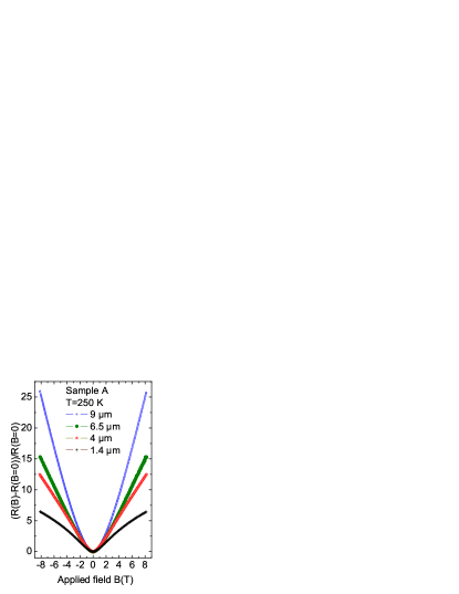
The magnetoresistance for fields normal to the graphene planes systematically decreases decreasing the constriction width, starting already with the largest as shown in Fig. 6 for sample A (similar behavior is obtained for sample B), as observed in bulk HOPG samples but at lower temperatures González et al. (2007). This behavior indicates that m up to room temperature. The field dependence of the Hall resistance as well as its temperature dependence in similar graphite flakes as presented in this work, deviate clearly from measurements in bulk graphite samples, see e.g. Ref. Du et al., 2005. Although the calculation of the carrier density through the Hall effect in semimetals due to the electron and hole contributions is non simple, the obtained results support not only the existence of the low carrier density but also the weak temperature dependence of . Finally, for fields parallel to the graphene planes and input current the magnetoresistance shows pronounced Aharonov-Bohm oscillations, similar to that found in Bi nanowires Nikolaeva et al. (2008) and topological insulators Peng et al. (2009), demonstrating the coherent propagation of electrons around a length of several micrometers up to temperatures K.Schadewitz et al.
We thank H. Peredo for technical support in the Hall effect measurements. This work is supported by the Deutsche Forschungsgemeinschaft under contract DFG ES 86/16-1; S.D. is supported by the Graduate School of Natural Sciences “BuildMoNa” of the University of Leipzig.
References
- Luk’yanchuk and Kopelevich (2004) I. A. Luk’yanchuk and Y. Kopelevich, Phys. Rev. Lett. 93, 166402 (2004).
- Li and Andrei (2007) G. Li and E. Y. Andrei, Nat. Phys. 3, 623 (2007).
- Orlita et al. (2008) M. Orlita, C. Faugeras, P. Plochicka, P. Neugebauer, G. Martinez, D. K. Maude, A.-L. Barra, M. Sprinkle, C. Berger, W. A. de Herr, et al., Phys. Rev. Lett. 101, 267601 (2008).
- Novoselov et al. (2005) K. S. Novoselov, A. K. Geim, S. V. Morozov, S. V. Dubonos, Y. Zhang, and D. Jiang, Nature 438, 197 (2005).
- Zhang et al. (2005) Y. Zhang, Y.-W. Tan, H. Störmer, and P. Kim, Nature 438, 201 (2005).
- Neto et al. (2009) A. H. C. Neto, F. Guinea, N. M. R. Peres, K. S. Novoselov, and A. K. Geim, Rev. Mod. Phys. 81, 109 (2009).
- Geim (2009) A. K. Geim, Science 324, 1530 (2009).
- Ouyang et al. (2010) Y. Ouyang, H. Dai, and J. Guo, Nano Res 3, 8 (2010).
- Sabio et al. (2008) J. Sabio, C. Seoánez, S. Fratini, F. Guinea, A. H. C. Neto, and F. Sols, Phys. Rev. B 77, 195409 (2008).
- García et al. (2010) N. García, Z. Yan, A. Ballestar, J. Barzola-Quiquia, F. Bern, and P. Esquinazi, Journal of Physics Condensed Matter 22, 045002 (2010).
- Morozov et al. (2008) S. V. Morozov, K. S. Novoselov, M. I. Katsnelson, F. Schedin, D. C. Elias, J. A. Jaszczak, and A. K. Geim1, Phys. Rev. Lett. 100, 016602 (2008).
- Du et al. (2008) X. Du, I. Skachko, A. Barker, and E. Y. Andrei, Nature Nanotech. 3, 491 (2008).
- Bolotin et al. (2008) K. I. Bolotin, K. J. Sikes, Z. Jiang, M. Klima, G. Fudenberg, J. Hone, P. Kim, and H. L. Stormer, Solid State Commun. 146, 351 (2008).
- Lin et al. (2009) Y.-M. Lin, K. A. Jenkins, A. Valdes-Garcia, J. P. Small, D. B. Farmer, and P. Avouris, Nano Lett. 9, 422 (2009).
- Miao et al. (2007) F. Miao, S. Wijeratne, Y. Zhang, U. C. Coskun, W. Bao, and C. N. Lau, Science 317, 1530 (2007).
- Arndt et al. (2009) A. Arndt, D. Spoddig, P. Esquinazi, J. Barzola-Quiquia, S. Dusari, and T. Butz, Phys. Rev. B 80, 195402 (2009).
- González et al. (2007) J. C. González, M. Muñoz, N. García, J. Barzola-Quiquia, D. Spoddig, K. Schindler, and P. Esquinazi, Phys. Rev. Lett. 99, 216601 (2007).
- García et al. (2008) N. García, P. Esquinazi, J. Barzola-Quiquia, B. Ming, and D. Spoddig, Phys. Rev. B 78, 035413 (2008).
- Barzola-Quiquia et al. (2008) J. Barzola-Quiquia, J.-L. Yao, P. Rödiger, K. Schindler, and P. Esquinazi, phys. stat. sol. (a) 205, 2924 (2008).
- Barzola-Quiquia et al. (2010) J. Barzola-Quiquia, S. Dusari, G. Bridoux, F. Bern, A. Molle, and P. Esquinazi, Nanotechnology 21, 145306 (2010).
- Wexler (1966) G. Wexler, Proc. Phys. Soc. London 89, 927 (1966).
- Stauber et al. (2007) T. Stauber, N. M. R. Peres, and F. Guinea, Phys. Rev. B 76, 205423 (2007).
- García and Escapa (1989) N. García and L. Escapa, Appl. Phys. Lett. 54, 1418 (1989).
- Snyman et al. (2008) I. Snyman, J. Tworzydło, and C. W. J. Beenakker, Phys. Rev. B 78, 045118 (2008).
- Costa-Krämer et al. (1997) J. L. Costa-Krämer, N. García, and H. Olin, Phys. Rev. Lett. 78, 4990 (1997).
- van Wees et al. (1988) B. J. van Wees, H. van Houten, C. W. J. Beenakker, J. G. Williamson, L. P. Kouwenhoven, D. van der Marel, and C. T. Foxon, Phys. Rev. Lett. 60, 848 (1988).
- Wharam et al. (1988) D. A. Wharam, T. J. Thornton, R. Newbury, M. Pepper, H. Ahmed, J. E. F. Frost, D. G. Hasko, D. C. Peacockt, D. A. Ritchie, and G. A. C. Jones, J. Phys. C: Solid State Phys. 21, L209 (1988).
- Brown (1970) R. D. Brown, Phys. Rev. B 2, 928 (1970).
- Yang et al. (2000) F. Y. Yang, K. Liu, K. M. Hing, D. H. Reich, P. C. Searson, C. L. Chien, Y. Leprince-Wang, K. Yu-Zhang, and K. Han, Phys. Rev. B 61, 6631 (2000).
- Zhang et al. (2000) Z. Zhang, X. Sun, M. S. Dresselhaus, J. Y. Yin, and J. Heremans, Phys. Rev. B 61, 4850 (2000).
- Drut and Lähde (2009) J. E. Drut and T. A. Lähde, Phys. Rev. B 79, 241405(R) (2009).
- Schneider et al. (2009) J. M. Schneider, M. Orlita, M. Potemski, and D. K. Maude, Phys. Rev. Lett. 102, 166403 (2009).
- Du et al. (2005) X. Du, S.-W. Tsai, D. L. Maslov, and A. F. Hebard, Phys. Rev. Lett. 94, 166601 (2005).
- Nikolaeva et al. (2008) A. Nikolaeva, D. Gitsu, L. Konopko, M. J. Graf, and T. E. Huber, Phys. Rev. B 77, 075332 (2008).
- Peng et al. (2009) H. Peng, K. Lai, D. Kong, S. Meister, Y. Chen, X.-L. Qi, S.-C. Zhang, Z.-X. Shen, and Y. Cui, Nature Mater. 9, 225 (2009).
- (36) A. Schadewitz, J. Barzola-Quiquia, A. Ballestar, and P. Esquinazi, to be published.