Defect-induced multicomponent electron scattering in single-walled carbon nanotubes
Abstract
We present a detailed comparison between theoretical predictions on electron scattering processes in metallic single-walled carbon nanotubes with defects and experimental data obtained by scanning tunneling spectroscopy of Ar+ irradiated nanotubes. To this purpose we first develop a formalism for studying quantum transport properties of defected nanotubes in presence of source and drain contacts and an STM tip. The formalism is based on a field theoretical approach describing low-energy electrons. We account for the lack of translational invariance induced by defects within the so called extended kp approximation. The theoretical model reproduces the features of the particle-in-a-box-like states observed experimentally. Further, the comparison between theoretical and experimental Fourier-transformed local density of state maps yields clear signatures for inter- and intra-valley electron scattering processes depending on the tube chirality.
pacs:
73.63Fg,73.22.-f,68.37.EfI Introduction
In the last two decades, carbon nanotubes discovered in 1991 Iijima:1991 and in particular Single-Walled Carbon Nanotube (SWNT) that emerged shortly Iijima and Ichihashi (1993); Bethune et al. (1993) after have attracted a continuously increasing interest from the solid states physics community due to their outstanding electronic and mechanical properties. Saito et al. (1998); Tomanék and Enbody (1999); Ando (2005); Charlier et al. (2007); Steele et al. (2009a); Lassagne et al. (2009) A single-walled carbon nanotube (SWNT) can be regarded as a strip of graphene rolled into a hollow cylinder with diameters typically in the order of one nanometer and lengths ranging from a few microns to a few centimeters. Charlier et al. (2007) Because of the very small diameter, a SWNT is generally considered as a quasi-one-dimensional system. SWNTs can be either metallic or semiconducting with energy bandgaps varying from zero to above 1 eV, depending on their geometrical structure. Charlier et al. (2007)
The low energy spectrum of metallic SWNT comprises four branches with a linear dispersion close to the charge neutrality point (CNP). Depending on the chirality, the corresponding electronic states can be degenerate in the orbital momentum. These states are symmetric with respect to the energy plane through the CNP implying electron-hole symmetry. Jarillo-Herrero et al. (2004) Other dispersive, energy symmetric electronic states are opening at higher energy, with a gap eV. All these electronic states can be obtained theoretically from a kp method. Ando (2005) This approach is particularly useful for studying transport properties.
An ideal metallic SWNT — defectless, charge-neutral and infinitely long — can be regarded as a quantum wire with four propagating one-dimensional conduction channels, i.e. two left- and two right-movers. note:one This leads to a quantized conductance at zero temperature of , since each left- or right-moving channel is two-fold degenerate in spin.
In practice, devices with pure and clean SWNTs are hardly achievable. Their structure is modified by random potentials arising from adsorbates, defects, inhomogeneous substrate interactions, Schottky barriers at contacts etc.. These perturbations lead to a finite backscattering probability and hence an experimentally measured conductance below the theoretical maximum of . The scattering mean-free path of SWNTs has been experimentally determined and is of the order of m. It is usually longer in metallic SWNTs and shorter in semiconducting ones. Charlier et al. (2007)
SWNTs constitute an ideal platform to study many body interactions in one-dimensional conductors. A field theoretical approach based on the Tomonaga-Luttinger liquid model Tomonaga (1950); Luttinger (1963) has been proposed a decade ago Egger and Gogolin (1997, 1998); Kane et al. (1997); Egger (1999) in order to describe interaction effects in isolated single-walled and multi-walled carbon nanotubes. Some experiments have reported on power-law behavior of the conductance as function of the applied voltage and/or the temperature for SWNTs Bockrath et al. (1999); Yao et al. (1999) and for metallic junctions of crossed SWNTs Gao et al. (2004) with exponents in the range of theoretical predictions.
Transport experiments on SWNTs cover several distinct regimes characterized by the number of external electrodes and the quality of the contacts between the electrodes and the tube. Source and drain electrodes drive an electric current through a contacted SWNT. These electrodes can be either weakly or strongly coupled to the nanotube. In the first case — the so-called Coulomb blockade regime — effects of Coulomb charging play an important role. Postma et al. (2001) Oppositely, for strong coupling — the so-called Fabry-Pérot regime Pugnetti et al. (2009) — the transmissivity of the contacts is close to unity Liang et al. (2001); Wu et al. (2007); Herrmann et al. (2007) therefore minimizing the effects of Coulomb charging. The use of a back gate permits to shift the position of the SWNT bands relative to the Fermi level in order to probe the conduction channels as a function of energy. In a typical strongly coupled two-terminal device, the SWNT differential conductance — the derivative of the average current with respect to the applied voltage — shows an oscillatory behavior as a function of the source-drain and gate voltages. These oscillations can be easily interpreted in terms of a Fabry-Pérot electron resonator model: Liang et al. (2001) at low energy the electrons propagate ballistically between the two contacts and the oscillation pattern of the differential conductance is the result of coherent interference.
Detailed investigations of transport and structural properties of SWNTs can be achieved by means of scanning probe techniques as, e.g., scanning tunneling microscopy/spectroscopy (STM/STS) or scanning gate microscopy (SGM). In both cases, an atomically sharp metallic tip is brought in close proximity to the nanotube. In this configuration, by applying a bias voltage it is possible to generate a tunneling current between the conductive sample and the tip. This current is kept constant by means of a feedback loop whose output signal adjusts the vertical -position of the tip as a function of the - position. The recorded signal reflects a constant current contour map — it can be interpreted, in a first approximation, as the topography of the sample. In STS, the tip is stopped at a given position and the feedback loop is switched off. The differential conductance is measured by sweeping the bias voltage between two values corresponding to two fixed energies. The knowledge of the differential conductance gives access to the local density of states (LDOS) of the sample. Tersoff and Hamann (1985)
STM/STS techniques allow the study of individual SWNTs lying on a conductive substrate Buchs et al. (2009); Ouyang et al. (2002); Venema et al. (1999); Lemay et al. (2001a) but also of SWNT devices with a source-drain and back-gate geometry. Leroy et al. (2007) In SGM, the biased tip — playing the role of a local gate — is scanned at fixed height over a SWNT device between source and drain contacts. Fan et al. (2005); Bockrath et al. (2001) The Fermi level of the tube is locally shifted due to charge accumulation near the tip and thus a map of the two-terminal transconductance of the nanotube device can be established. In all these cases, the tip couples weakly to the SWNT. A strong coupling regime can be reached with a conductive atomic force microscope (AFM) tip brought in contact with the nanotube in order, e.g., to perform length-dependent two-terminal conductivity measurements. depablo:2002
In this paper, we first investigate theoretically the transport properties of strongly coupled SWNT devices — perfect source and drain contacts — with a third terminal, experimentally realized by a conductive tip in the weak coupling regime. In absence of translational invariance due to the presence of scattering centers, we develop a general formalism for studying electron scattering within the so-called extended kp model. We account for scattering centers such as structural defects, tube ends or arbitrary random potentials. The approach leads to a general scattering matrix formulation of transport properties — current and differential conductance — of imperfect SWNTs. We apply our method to the case of a low temperature STM/STS experiment. In this set-up, individual finite-length metallic SWNTs dispersed on a gold substrate show particle-in-a-box states between consecutive scattering centers. Our approach permits a fundamental understanding of the nature of the observed scattering patterns in reciprocal space. Buchs et al. (2009)
The paper is organized in the following way: in Sec. II we give an overview of the electronic properties of SWNTs in the kp approximation as well as in the extended kp approximation accounting for the presence of scattering centers; in Sec. III we employ a field theoretical approach and the extended kp model to develop a method suitable to study the quantum transport properties of imperfect metallic SWNTs; in Sec. IV we describe the experimental setup, the sample preparation, and the Fourier transform STS technique used for data analysis; in Sec. V we compare the results of theory and experiment for the case of diverse SWNTs.
II The extended kp model
A SWNT can be regarded — from the geometrical point of view — as a single-layer graphene strip rolled into a cylinder. Its structure is generally indexed by its chiral vector defined by the circumferential vector that starts and ends on the same lattice site of the SWNT (see e.g. Refs. [Saito et al., 1998; Ando, 2005]). The circumferential vector can be expressed as a linear combination of the two basis vectors and of the honeycomb lattice, where is the lattice constant ( nm is the bond length between carbon atoms). Thus, , and the geometry of a SWNT is completely defined by the pair of integers — the chiral indices. The diameter of a SWNT is given by:
| (1) |
The unit cell of a SWNT is defined by the chiral vector and the translational vector perpendicular to . The translational vector is the smallest lattice vector that leaves the SWNT lattice invariant when shifted by T along the axis and its norm
| (2) |
defines the translational period. Here is the greatest common divisor of and . The nanotube unit cell is thus formed by a cylindrical section of length and diameter . It contains carbon atoms.
To understand the electronic properties of SWNTs, a simple way is to start with the band structure of graphene. This can be obtained from an effective tight-binding model with nearest-neighbor hopping with hopping integral eV. Charlier et al. (2007) The first Brillouin zone of the honeycomb lattice is characterized by the reciprocal lattice vectors and . Only two out of six vertices of the first Brillouin zone are non-equivalent — the and points. A common choice is usually and . The conduction and valence bands formed by -states touch at these and points. Due to periodic boundary conditions around the circumference of a SWNT, the allowed wave vectors perpendicular to the tube axis are quantized. In contrast, the wave vectors parallel to the tube axis remain continuous under the assumption of an infinitely long tube. The imposition of periodic boundary conditions in transverse direction leads to the following constraint on the electronic wavefunction:
| (3) |
where is a vector on the tube surface and lies in the first Brillouin zone of the nanotube. Thus, the electronic states are restricted to vectors that fulfill the condition:
| (4) |
with integer. Here is the circumferential component of the electron momentum. Plotting the endpoints of these allowed vectors for a given SWNT in the reciprocal space of graphene generates a series of parallel and equidistant lines. The distance between the lines is . The length, number and orientation of these lines depend on the chiral indices of the SWNT. If we restrict the wave vectors to the first Brillouin zone of the nanotube, its length is found to be and the number of lines is equal to . The electronic band structure of a specific nanotube is given by the cuts of the graphene electronic energy bands along the corresponding allowed -lines: we find a pair of conduction (antibonding) and valence (bonding) bands for each -line (zone folding). Therefore, if the graphene and points are crossed by an allowed -line, the SWNT is metallic, otherwise it is a semiconductor.
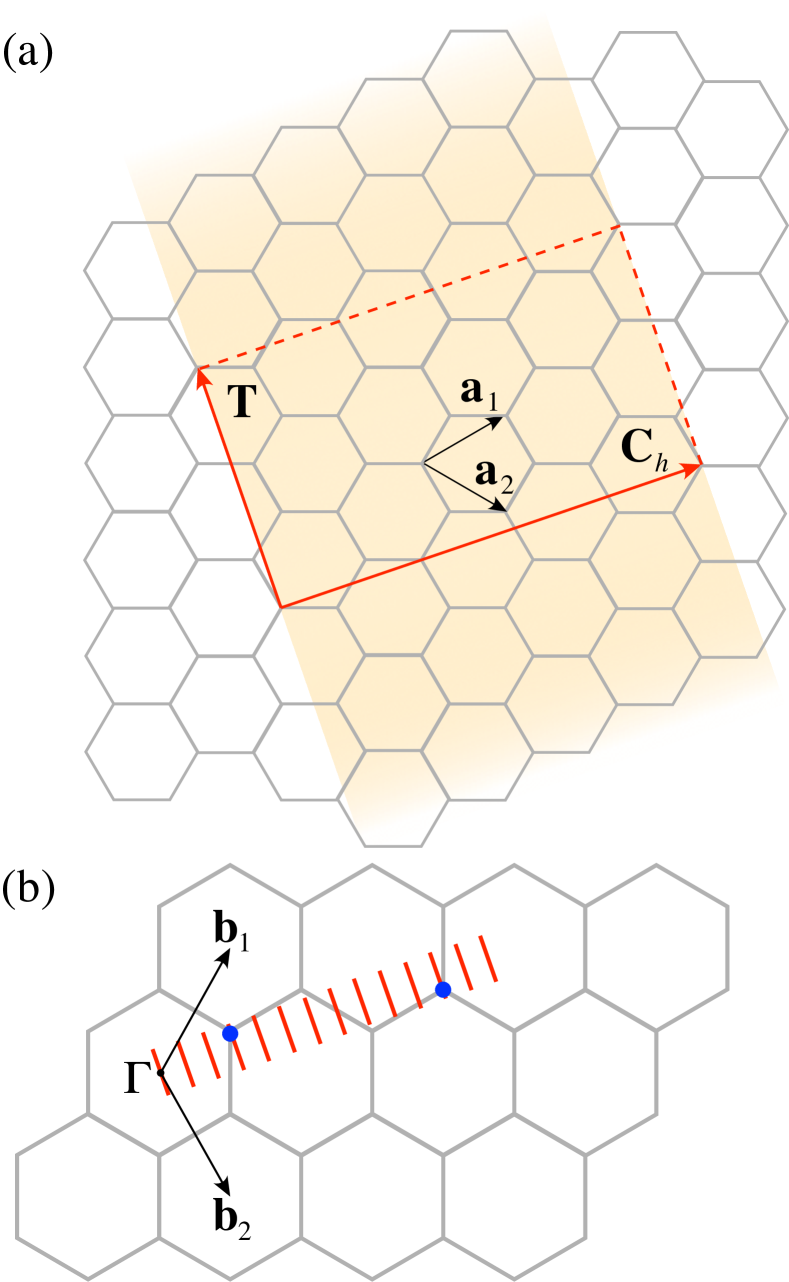
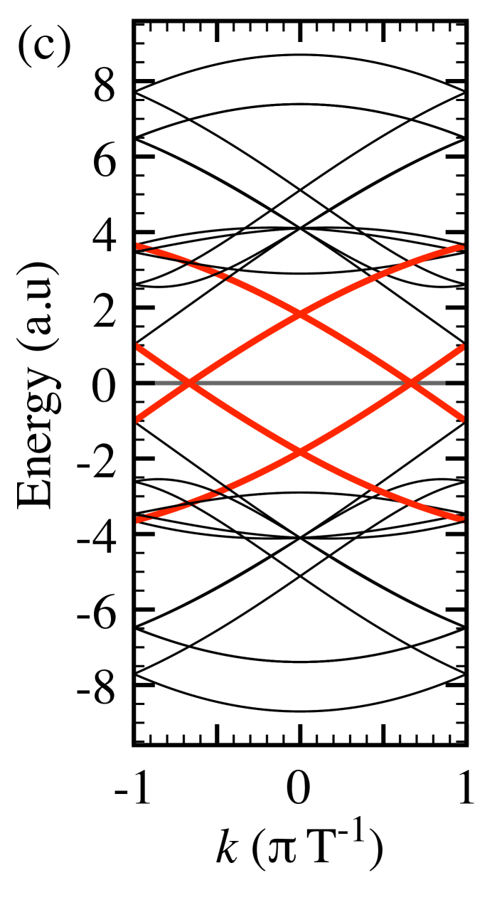
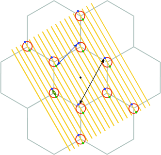
In Fig. 1(a) and (b) we show the case of a SWNT in the real and reciprocal space, respectively. Starting from the -point we have a set of 14 parallel lines that are touching the vertices of the reciprocal honeycomb lattice in two points marked with dots — the is then a metallic SWNT. note:two In Fig. 1(c) we show the energy spectrum with energies measured relative to the CNP. The lines touching the dots representing and of Fig. 1(b) are mapped in a set of bands (thick lines) crossing at the CNP. Around the CNP these bands have a quasi-linear behavior with respect to the momentum. Near the two -points where the energy becomes very small, it is possible to perform an effective-mass or kp approximation. Here, the wavefunction is factorized in a slowly-varying part — containing information about the lattice topology — times a plane wave. In this limit, the energy spectrum around each of the points reads
| (5) |
where is the effective Fermi velocity — the slope of the bands around zero energy. Here is the longitudinal component of the momentum relative to the -points. The total longitudinal component of the electron momentum is (). The energy spectrum (5) presents a four-fold degeneracy: a two-fold one due to the presence of two independent -points, and a two-fold one related to the electron spin. This degeneracy leads to the fundamental result that the conductance at zero temperature is quantized and equal to for ideal ohmic contacts.
So far we have considered the properties of a perfect, infinitely long SWNT. However, this is the exception, in reality we usually are faced with tubes with imperfections, in particular defects in the atomic structure. These correspond in some cases to simple vacancies of one or more carbon atoms, Charlier et al. (2007) or lattice distorsions like Stone-Wales defects. Stone and Wales (1986) Adatoms (C, H, N…) also modify the chemical structure of SWNTs. Buchs et al. (2007a); Buchs_Ar In the presence of defects, the translational invariance of the SWNTs is broken. This implies that the electronic spectrum cannot simply be calculated by applying Bloch’s theorem as done previously.
In the following we provide an approach tackling the problem of quantum transport in SWNTs in the presence of defects. First we need to define the important length scales of the problem. A defect will distort the lattice structure of a SWNT in a region around the defect site characterized by a typical length, the effective size of the scatterer. This has to be compared with other characteristic lengths of SWNTs such as the diameter , the translational period , and the atomic lattice spacing . In addition, defects and impurities give rise to an effective scattering potential with a potential strength . This has to be compared with the effective hopping strength between carbon atoms. In the following we assume that the effective size of the scatterer is smaller than the SWNT diameter , and that the impurity potential is smaller than the hopping strength .
Let us start with some considerations concerning the smallest of the characteristic length scale of a SWNT: the lattice constant . In presence of long-range defects backscattering within the same valley or between different valleys is suppressed. This effect — known also as Klein tunneling — has been predicted in SWNTs for the first time in 1998 by Ando and Nakanishi Ando and Nakanishi (1998) and has recently been observed in SWNT quantum dots. Steele et al. (2009b) On the other hand, if the effective size of the defects is comparable to the lattice constant , backscattering within the same valley — intra-valley scattering — and between different valleys — inter-valley scattering — become relevant. These scattering mechanisms become in general exponentially suppressed as the effective size of the defect grows.Ando (2005)
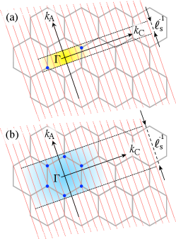
In order to understand how to go beyond the aforementioned standard kp model when dealing with defected SWNTs, we have to recall the role played by translational invariance in presence of umklapp processes. These processes are characterized by exchanged momenta exceeding in modulus the length of the reciprocal lattice vectors — the electrons are scattered into a different Brillouin zone of the reciprocal lattice. For a translationally invariant system, the equivalence of wave vectors differing by a reciprocal lattice vector allows to reduce these scattering events to the first Brillouin zone. Ando (2005)
Defects change drastically this physical picture: the translational invariance is broken and wave vectors differing by reciprocal lattice vectors are no longer equivalent. We illustrate this situation in Fig. 2. Here we show the honeycomb reciprocal lattice and the parallel lines due to the periodic boundary conditions (3). In order to understand the consequences of the lack of translational invariance, we consider two distinct cases: in panel (a), and in panel (b). The area of influence of defects in the reciprocal space is represented as a shadow area of approximative width . The precise extent of this area will depend on the details of the shape of the Fourier transform of the defect potential. For a single defect, this is in general a decreasing function of the distance from the point. In case (a), scattering events induced by the defect produce an exchanged momentum smaller than any reciprocal lattice vector. This is usually the regime in which backward scattering is suppressed — therefore the scattering processes can all be studied within the original first Brillouin zone of the translationally invariant case. In this approximation we can adopt the conventional kp picture. However, in case (b) this is no longer valid: defects induce scattering processes with exchanged momenta exceeding the size of the original first Brillouin zone. Hence, we have to account explicitly for all processes within a new extended scattering zone whose dimensions are given by the inverse effective size of the scatterer. In the extended kp approach we allow for new scattering channels that are associated with exchanged momenta larger than the difference between the original points. We refer to this consequences of broken translational symmetry as multi-component scattering. The exchanged momentum of each of these scattering processes will be characterized by an axial and a circumferential component, respectively (c.f. Fig. 4). This approach will be detailed in the following section.
III Model Hamiltonian and scattering Processes
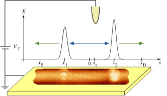
We consider now a metallic SWNT device with ideal ohmic contacts to source (S) and drain (D) as well as a weak tunneling contact to a third electrode. In our case this is an atomically sharp STM tip, henceforth denoted as tip (T). The SWNT has a finite length and for the coordinate along it we choose the origin in the middle of the nanotube so that the interfaces to the S and D electrodes are located at and , respectively. In the tube we account for the presence of several defects characterized by an effective size comparable to the lattice constant . The tip is described as a semi-infinite non-interacting Fermi gas, and denotes the coordinate axis along the tip orthogonal to the tube, the origin corresponding to the injection point on the tip. The latter is located at position with respect to the middle of the tube, and electron injection is modeled by a tunneling Hamiltonian.
The total Hamiltonian of the system reads
| (6) |
where the first term describes the defected SWNT and the coupling to the S and D leads. The second term accounts for the tip, whereas the last one includes SWNT-tip tunneling.
Concerning the SWNT, we focus on the low-energy excitations: the energy spectrum is considered as linear with respect to the electron momentum around the CNP (c.f. Eq. (5)). The electron operator can be decomposed around each of the two Dirac points into right- and left-moving components and , respectively. The electron field reads
| (7) |
where denotes the equilibrium Fermi momentum of the SWNT with respect to the charge neutrality point . The Hamiltonian for the SWNT reads
| (8) |
In the previous equation the first term
| (9) |
describes the band linearized spectrum (5). The symbol stands for normal ordering with respect to the equilibrium ground state. The second term in Eq. (8) models impurity scattering. In the low-energy approximation, impurities with an effective size comparable to the lattice constant can be approximated by delta-like impurities. In order to fully account for the extended kp model introduced in the previous section we have to account for multi-component scattering: Each of these impurities can either scatter electrons within the same valley — intra-valley scattering — or can change the valley index of the backscattered electrons — inter-valley scattering. In addition, we have to account for extended inter-valley scattering processes where the exchanged momenta are larger than the difference between the K points. In terms of field operators, the scattering Hamiltonian within the extended kp model is of the form
| (10) | ||||
with and . Here terms with describe forward scattering processes and terms with describe backscattering. Moreover, for we have intra-valley scattering while terms with describe inter-valley scattering. Finally, is a reciprocal lattice vector and describes extended inter-valley scattering processes. For a particular case, the various scattering processes are sketched in Fig. 4. In practice, the coupling constant will depend on the Fourier transform of the scattering potential of the –th defect. Hence, for a given defect the coefficient differs for each of the available scattering processes. Also the range of -terms to be summed over depends on the spatial extend of the defects. We will allow for several defects at positions .
The third term in Eq. (8) accounts for the source and drain electrodes
| (11) |
with
| (12) |
where the term is the electron density fluctuation with respect to the equilibrium value.
The Hamiltonian of the tip, the second term in Eq. (6), reads
| (13) |
Here
| (14) |
describes the (linearized) band energy with respect to the equilibrium Fermi points of the tip, and denotes the Fermi velocity. Notice that the integral runs also over the positive -axis, since right and left moving electron operators along the physical tip axis have been unfolded into one chiral (right-moving) operator defined on the whole -axis. The second term in Eq. (13) describes the bias applied to the tip that affects the incoming electrons according to
| (15) |
Finally, the third term in Eq. (6) accounts for the SWNT-tip tunneling and reads
| (16) | ||||
where is the tunneling amplitude for electrons, and [] is the coordinate of the injection point along the tube [tip].
In the following we will evaluate the differential conductance in the tip terminal of the described set-up. Explicitly, due to the unfolding procedure described above, the electron current flowing in the tip at a point acquires the form
| (17) |
Since the system Hamiltonian (6) is quadratic in the fields and it admits an exact solution. In fact, we can determine the transport properties within the Landauer-Büttiker formalism. Büttiker (1986); Pugnetti et al. (2009) In the three-terminal set-up the energy-dependent scattering matrix is a matrix. It is a function of the tip position, the applied tip-SWNT bias, and the exchanged momenta in the scattering processes described by the extended kp model. The axial component of determines the momentum exchanged by the electrons along their direction of motion. On the other side, the circumferential component of affects — via the values of — the strength of the scattering process. In the following the scattering matrix is expressed by the simplified notation
| (18) |
where the energy is measured with respect to the CNP. The scattering matrix is obtained by solving the equations of motion for the system formed by the SWNT and the tip of the STM. The current flowing through the tip from the SWNT may be written as
| (19) |
with
| (20) | ||||
Here , , and are the Fermi distribution functions for the source, drain and tip contacts, respectively.
In the low temperature STM/STS experiment described in the next section, the differential conductance is deduced from the current flowing through the tip terminal. In addition, in the experimental set-up the metallic SWNT lays on a gold substrate, therefore its potential is uniform along the tube length. In our formalism this corresponds to the case of chemical potentials of source and drain electrodes fixed to the same value, so that . Given these conditions, the differential conductance can be readily obtained from Eq. (19). At zero temperature we have
| (21) |
This is a function of the tip position and the voltage applied between the SWNT and the tip.
We want to add an important remark about the validity of the result (21) for the differential conductance. The strong contact between the metallic SWNT and the gold substrate is ruling the phenomena observable experimentally — this leads to a short lifetime of electrons injected from the tip into the SWNT. rubio:1999:a ; rubio:1999:b Taking into account that experiments are performed at 4 K and that the applied voltages correspond to even larger energies, effects due to interactions with an energy scale smaller than cannot be resolved in the local density of states. eggert:2000 In addition, the gold substrate is also partially screening the electronic Coulomb interaction in the SWNT and the tunneling junction resistance is dominating over the experimental set-up resistive circuit therefore excluding effects as the dynamical Coulomb blockade. devoret:1990 Therefore, the only effect of interaction that we take explicitly into account is a renormalization of the Fermi velocity egger:1997 in Eq. (9). Within this reasonable approximation the result (21) is valid and will suffice to describe the experimental observations.
IV Experiments
In the following section, we use our model to study the electronic interference patterns observed in the LDOS both in real and reciprocal spaces between artificially created scattering centers on metallic SWNTs deposited on a conductive substrate. In the next three sections we give a brief introduction to the experimental set-up and the data analysis technique.
IV.1 LT-STM/STS setup
The experiments have been carried out in a commercial LT-STM set-up (Omicron) operating in ultra high vacuum (UHV) with a base pressure below 10-10 mbar. The STM topography images have been recorded in the constant current mode. In this set-up we refer to sample bias being the potential difference between the grounded sample and the tip. We used mechanically cut Pt/Ir tips for the topographic scans and the spectroscopy measurements, where the metallic nature of the tips has been regularly checked on the conductive substrate. Differential conductance spectra — proportional to the LDOS in first approximation Tersoff and Hamann (1985) — were measured using the lock-in technique. Under open loop conditions a low amplitude a.c. bias (5-15 mV at 600 Hz) is added to the sample bias and the resulting a.c. component of the tunneling current is detected. All the measurements have been carried out at a temperature of 5 K. All STM topography images presented in this work have been treated with the open source WSXM software. Horcas et al. (2007)
IV.2 Sample preparation
Gold on glass substrates have been used to support the SWNTs for the measurements. In order to obtain clean Au (111) monoatomic terraces, the gold surface has been prepared by several in situ sputtering and annealing cycles. The SWNTs provided from Rice University were grown by the high pressure CO disproportionation process (HiPco) and purified. Chiang et al. (2001) To maximize the number of individual nanotubes, the raw material was sonicated for 2-3 h in 1,2-dichloroethane and a droplet of the obtained SWNT suspension was then deposited ex situ on the well prepared gold surface. Finally, residues from the solvent of the suspension were removed in situ by means of a short sample annealing at about 390 ∘C. More details on the sample preparation can be found in Ref. [Buchs et al., 2007b].
Strong electron scattering centers were created by two methods: bombardment with medium energy Ar+ ions inducing vacancy-type defects, Gómez-Navarro et al. (2005); Tolvanen:2009 whereas voltage pulses in the STM created cuts of the SWNT at the tip position. In the former case, we used a standard Leybold™ ion gun designed to be integrated with the preparation chamber of the STM setup. The ion gun and exposition parameters needed to achieve a defect density along the tube axis of about 0.1 nm-1 have been obtained from irradiation tests performed on a freshly cleaved graphite (HOPG) substrate, as described in details in Ref. [Tolvanen:2009, ]. In order to create short SWNT segments, we have made use of the technique reported earlier by Lemay et al. in Ref. [Lemay et al., 2001b] where nanotubes were cut by applying a local voltage pulse of about V at constant height (open loop). It is known that the ultrasonication process used to disperse the nanotubes can also introduce defects. However, we checked the tubes before ion bombardment and found at most one defect every 200 nm. Since we aimed at a density of one defect per 10 nm, not more than one out of twenty defects was introduced by the ultrasonication process. The precise creation of a scattering defect is in fact not of much relevance for the electron scattering processes discussed here.
IV.3 Real and reciprocal space measurements
Electronic interference patterns induced between consecutive scattering centers are measured by recording a series of equidistant STS spectra along the SWNT. In a first approximation, these give information about the LDOS along the tube axis. Tersoff and Hamann (1985) Typical data sets — called -scans in the following — generally consist of 150 spectra recorded on topography line scans of 300 pts.
Insights into the electron scattering leading to the interference patterns are obtained in the reciprocal space by means of the Fourier transform STS technique. Here, line-by-line zero-padding Fourier transforms of the -scans are performed in the spatial region of interest — generally between two consecutive scattering centers — where the offset amplitude of each line has been subtracted. In order to avoid aliasing effects in the resulting data set, we always make sure to fulfill the sampling theorem. This requires that the highest spectral component of a signal must be smaller than , where is the spatial sampling frequency. Shannon (1949) This frequency is defined as where is the distance between two consecutive measurement points in the -scan. For our purpose, we can show that for the usual spacing nm in a -scan, the relevant spectral features with nm-1 are guaranteed free of aliasing effects up to the maximum analyzed length of about 20 nm. Buchs et al. (2009)
Note that the spatial extent of a -scan generally acquired within a time frame of about 30 min is always observed to be slightly larger (of the order of 5%) than the spatial extent of the successive (or previous) topography lines acquired within about 0.5 s, due to a dependency of the piezoelectric voltage constant on the scan velocity. This effect has been systematically corrected by a compression of the -scale of the -scan to allow for a consistent comparison between the topographic and spatially resolved spectroscopic information on the same nanotube.
V Comparison between Theory and Experiment
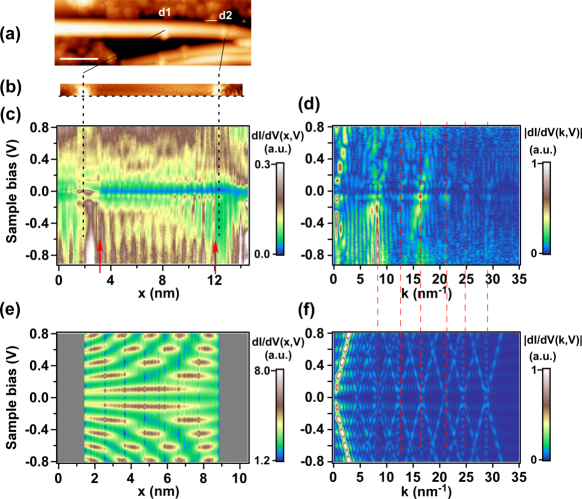
The first experimental example to which we applied our model is illustrated in Fig. 5. Panel (a) shows the topography image of a nm long portion of a metallic SWNT that has been exposed to a low dose of keV Ar+ ions. Tolvanen_Ar; Buchs et al. (2009) A detail image of the zone delimited by the pair of defects labeled d1 and d2 is displayed in (b). Defects induced by medium energy Ar+ ions appear typically as hillocks with an apparent height ranging from Å to Å and a lateral extension between Å and Å. We have shown in an earlier work Tolvanen:2009 , by means of a detailed comparison of the spectroscopic signature of defect sites with predictions of ab-initio simulations, that 1.5 keV Ar+ ion bombardment of semiconducting SWNTs mainly gives rise to single and double vacancies, C-adatoms as well as combinations of these individual species. For metallic tubes the same defect structures are expected, but because of prohibitively high computational costs, the exact structure of defects in metallic SWNTs can hardly be determined with high accuracy. However, since the effective size of these defects is comparable to the lattice constant , they can approximately be treated as delta-like impurities with a given scattering strength as presented in Sec. III. We will show later in this section that this simplified approach is accurate enough to interpret our experimental data to a large extent. In Panel (c) of Fig. 5 we shows the corresponding -scan recorded along the horizontal dashed line in Panel (b). The map resulting from a line-by-line zero padding Fourier transform performed between the positions indicated by the two red arrows drawn in (c) is depicted in (d). The low frequency Fourier spots positioned between nm-1 and nm-1 correspond to intra-valley scattering processes. Buchs et al. (2009) They are characterized by an average energy separation of 160 meV. This is in agreement with the value 169 meV resulting from the one dimensional particle-in-a-box model for the linear dispersion of a metallic nanotube ( around the inequivalent Fermi points). The energy spacing can be obtained by
| (22) |
with nm and the Fermi velocity m/s. Lemay et al. (2001b)
The more intense dispersive features allowing for intervalley scattering are visible around nm-1 and at nm-1. Further dispersive sets of spots are visible around nm-1, nm-1 , nm-1 and nm-1. The left-right asymmetry of the interference pattern in the experimental -scan (Fig. 5c) can be attributed to different scattering strengths of the defect sites d1 and d2. Buchs et al. (2009) From atomically resolved topography images of the nanotube we can determine a chiral angle of . Based on this value of the chiral angle and the position of the Fourier spots in the map, we find a good match with a (14,5) metallic SWNT (). Panel (e) displays the calculated differential conductance for a (14,5) SWNT with inter-defects length nm and asymmetric impurity strengths and . In general, each of the coefficients in Eq. (10) depends on the Fourier transformed scattering potential of the defect in question. Here we assume that this Fourier transform can adequately be described by a simple Gaussian. The interference patterns show characteristic stripes with increasing curvature when moving form the weaker left to the stronger right impurity. Buchs et al. (2009) All the observed Fourier components in (d) are reproduced in the calculated map in (f). The comparison between experiment and theory shows that regarding the positions and slopes of the scattering related branches close correspondence is found for the Fourier transformed -scans. The intensity of the branches is, however, not well reproduced by the theory, which is the reason for a less pronounced agreement between the spatial -maps. This is mainly due to the fact that in reality the scattering strength of a defect will depend on energy, momentum and pseudo-spin in a complex manner, which is not reproduced by the simplified delta-like scattering potential of our theoretical model. Nevertheless, the agreement between the Fourier transforms of the theoretical (f) and experimental (d) -scans clearly proves that the model well reproduces the effect of multi-component scattering in metallic SWNTs. In the experiment, an asymmetry in the intensity of the positive and negative slope branches of the scattering process can be observed. In the experiment an asymmetry in the intensity of the positive and negative slope branches of the scattering process. The dispersion lines show a more intense signal for the positive slope branch than for the negative one. This asymmetry can be ascribed to a breaking of the particle-hole symmetry due to lattice reconstruction that mixes the two carbon sub-lattices of the SWNT structure at the defect site. Mayrhofer and Bercioux (2010)
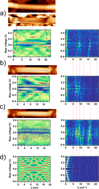
A second example is illustrated in Fig. 6. Panel (a) displays a 23 nm long section of a metallic SWNT irradiated with 200 eV Ar+ ions showing two defect sites separated by nm. The -scan shows well-defined modes with an energy spacing of about 100 meV as expected from the separation of the two defects. In contrast to the example above, the interference pattern does not show curved stripes. This indicates that in this case the scattering strengths of the two defects are similar. There is however a discernible symmetry breaking with respect to the -axis at , which should be the position of a mirror-axis. This points to different scattering phase shifts at the two defect sites. Note that our Fabry-Pérot model does not take the phase shift into account. When the tube is cut at both defect sites as shown in panel (b), the mode pattern develops the typical asymmetric stripe pattern, which we found to be characteristic for different scattering strengths (here with ). Buchs et al. (2009) A further cutting pulse close to the left end of the tube results in the disappearance of the asymmetry as shown in panel (c). It also leads to a weaker resonant modes pattern, indicating a reduction of the scattering strength at the left end of the tube. The left and right ends have now similar scattering strengths.
This sequence of experiments indicates that even though one can expect tube ends to be hard potential walls for the electrons, the scattering strengths at tube ends can be different. This might result from different effects, e.g., due to different symmetry properties of the tube ends or due to a stronger tube–substrate interaction at the tube end. The latter can be induced by the cutting procedure, leading to electron absorption instead of scattering. Furthermore, one can notice that the maps corresponding to the three cases (a), (b), and (c) show intervalley scattering patterns with different intensities with some of them almost suppressed. To allow a better analysis of these changes, we used our model to calculate the differential conductance for a 20 nm long SWNT portion and the corresponding map for symmetric scattering strengths at both ends (d). The best match was found for a metallic (10,4) nanotube. Out of the nine projected Fermi cones included in the extended kp model [one right/left movers branch with a positive/negative slope and a dispersiveless branch corresponding to forward scattering processes], about six cones are visible in the maps of the three cases presented in Fig. 6. In each case, some of the cones are almost suppressed and some show a higher intensity. Also, in this case we observe that some of the presented cones display only one dispersive slope. We can interpret these observation again in terms of breaking of the particle-hole symmetry. In fact in the tube ends several hexagons are substituted by pentagons, Saito et al. (1998) this results in a direct bonding of carbon atoms on the same sub-lattice of the SWNT structure. Mayrhofer and Bercioux (2010)
VI Conclusions
We have presented a general method for studying electron scattering in metallic SWNTs in presence of defects. In particular, we focused on the presence of defects characterized by an effective size of the order of the SWNT lattice constant. In this limit, translational invariance is broken implying that the properties of SWNTs cannot be obtained from the Bloch theorem. We have shown that it is possible to introduce an extended kp model in which the momentum exchanged in scattering processes can exceed the first Brillouin zone and cover an extended region depending on the effective size of defects. Within this scheme several scattering channels are available for electrons: intra- and inter-valley scattering in addition to extended inter-valley scattering. The latter becomes relevant because of the lack of translational invariance.
We have studied the consequences of this kind of defects on the electronic properties of a metallic SWNT contacted by source and drain electrodes. Further, we have accounted for a weak coupling to a tip. Based on a field theoretical approach describing low-energy electrons, we have obtained a general relation for the differential conductance between the SWNT and the tip, which provides access to the modifications of the local density of states induced by defects. We have compared the results of our theoretical model for the local density of states with the results of experiments where — via the STM/STS technique — the same quantity has been measured in defected or finite length metallic SWNTs. In the experimental set-up defects have been created via Ar+ ion bombardment, while finite length tubes have been obtained by means of the pulsed-voltage cutting technique. The experimental results clearly show two important features of the theoretical approach. Firstly, the particle-in-a-box-like states observed experimentally between consecutive defects are well described by a model with linear dispersion for electrons close to the CNP. In accordance with the model, the measured level spacing depends only on the distance between successive defects. Secondly, the extended kp approach fully succeeds in explaining the features observed in the Fourier transformed local density of states. This includes characteristics coming from intra- and inter-valley scattering as well as these associated with extended inter-valley scattering. Within this model the chiral angle determines uniquely the momenta exchanged in the scattering events causing the structure of the Fourier transformed local density of states. We have shown that the angle obtained from this procedure is in agreement with the one measured experimentally by atomically resolved topography images of SWNTs.
In spite of these assets, the model for the impurities we have introduced in our theory fails in catching one essential feature observed experimentally in the Fourier transformed density of states. Specifically, we have routinely observed an enhancement of some scattering channel with respect to others. These features can be explained by a more elaborate atomistic description of defects accounting for a possible breaking of the particle-hole symmetry due to lattice reconstruction at the defect sites. Mayrhofer and Bercioux (2010)
Acknowledgements.
We gratefully acknowledge helpful discussions with A. De Martino, M. Grifoni, P. Gröning, O. Johnsen, S. G. Lemay, L. Mayrhofer, T. Nakanishi, Y. Nazarov, D. Passerone, C. Pignedoli, P. Ruffieux and Ch. Schönenberger. OG acknowledges financial support by the CabTuRes project funded by Nano-Tera.ch. The work of DB and HG is supported by the DFG grant BE 4564/1-1 and by the Excellence Initiative of the German Federal and State Governments.References
- (1) S.Iijima, Nature 354, 56 (1991).
- Iijima and Ichihashi (1993) S. Iijima and T. Ichihashi, Nature 364, 737 (1993).
- Bethune et al. (1993) D. Bethune, C. Kiang, M. Devries, G. Gorman, R. Savoy, J. Vazquez, and R. Beyers, Nature 363, 605 (1993).
- Saito et al. (1998) R. Saito, G. Dresselhaus, and M. Dresselhaus, Physical Properties of Carbon Nanotubes (Imperial College Press, London, 1998).
- Tomanék and Enbody (1999) D. Tomanék and R. Enbody, Science and Application of Nanotubes (Kluwer Academic, Dordrecht, 1999).
- Ando (2005) T. Ando, J. Phys. Soc. Jpn. 74, 777 (2005).
- Charlier et al. (2007) J.-C. Charlier, X. Blase, and S. Roche, Rev. Mod. Phys. 79, 677 (2007).
- Steele et al. (2009a) G. A. Steele, A. K. H ttel, B. Witkamp, M. Poot, H. B. Meerwaldt, L. P. Kouwenhoven, and H. S. J. van der Zant, Science 325, 1103 (2009a).
- Lassagne et al. (2009) B. Lassagne, Y. Tarakanov, J. Kinaret, D. Garcia-Sanchez, and A. Bachtold, Science 325, 1107 (2009).
- Jarillo-Herrero et al. (2004) P. Jarillo-Herrero, S. Sapmaz, C. Dekker, L. P. Kouwenhoven, and H. S. J. van der Zant, Nature 389, 429 (2004).
- (11) It has been recently shown that ultraclean metallic SWNT can show a Mott insulating phase. V. V. Deshpande et al., Science 323, 106 (2009).
- Tomonaga (1950) S. Tomonaga, Prog. Theor. Phys. 5, 544 (1950).
- Luttinger (1963) J. Luttinger, J. Math. Phys. 4, 1154 (1963).
- Egger and Gogolin (1997) R. Egger and A. Gogolin, Phys. Rev. Lett. 79, 5082 (1997).
- Egger and Gogolin (1998) R. Egger and A. Gogolin, Eur. Phys. J. B 3, 281 (1998).
- Kane et al. (1997) C. Kane, L. Balents, and M. P. A. Fisher, Phys. Rev. Lett. 79, 5086 (1997).
- Egger (1999) R. Egger, Phys. Rev. Lett. 83, 5547 (1999).
- Bockrath et al. (1999) M. Bockrath, D. Cobden, J. Lu, A. Rinzler, R. Smalley, L. Balents, and P. McEuen, Nature 397, 598 (1999).
- Yao et al. (1999) Z. Yao, H. Postma, and C. Dekker, Nature 402, 273 (1999).
- Gao et al. (2004) B. Gao, A. Komnik, R. Egger, D. C. Glattli, and A. Bachtold, Phys. Rev. Lett. 92, 216804 (2004).
- Postma et al. (2001) H. W. C. Postma, T. Teepen, Z. Yao, M. Grifoni, and C. Dekker, Science 293, 76 (2001).
- Pugnetti et al. (2009) S. Pugnetti, F. Dolcini, D. Bercioux, and H. Grabert, Phys. Rev. B 79, 035121 (2009).
- Liang et al. (2001) W. Liang, M. Bockrath, D. Bozovic, J. H. Hafner, M. Tinkham, and H. Park, Nature 411, 665 (2001).
- Wu et al. (2007) F. Wu, P. Queipo, A. Nasibulin, T. Tsuneta, T. H. Wang, E. Kauppinen, and P. J. Hakonen, Phys. Rev. Lett. 99, 156803 (2007).
- Herrmann et al. (2007) L. G. Herrmann, T. Delattre, P. Morfin, J.-M. Berroir, B. Plaçais, D. C. Glattli, and T. Kontos, Phys. Rev. Lett. 99, 156804 (2007).
- Tersoff and Hamann (1985) J. Tersoff and D. R. Hamann, Phys. Rev. B 31, 805 (1985).
- Buchs et al. (2009) G. Buchs, D. Bercioux, P. Ruffieux, P. Gröning, H. Grabert, and O. Gröning, Phys. Rev. Lett. 102, 245505 (2009).
- Ouyang et al. (2002) M. Ouyang, J.-L. Huang, and C. M. Lieber, Phys. Rev. Lett. 88, 066804 (2002).
- Venema et al. (1999) L. Venema, J. Wildoer, J. Janssen, S. Tans, H. Tuinstra, L. Kouwenhoven, and C. Dekker, Science 283, 52 (1999).
- Lemay et al. (2001a) S. Lemay, J. Janssen, M. van den Hout, M. Mooij, M. Bronikowski, P. Willis, R. Smalley, L. Kouwenhoven, and C. Dekker, Nature 412, 617 (2001a).
- Leroy et al. (2007) B. J. Leroy, I. H., V. K. Pahilwani, , C. Dekker, and S. G. Lemay, Nano Lett. 7, 3138 (2007).
- Fan et al. (2005) Y. Fan, B. R. Goldsmith, and P. G. Collins, Nature Mater. 4, 906 (2005).
- Bockrath et al. (2001) M. Bockrath, W. Liang, D. Bozovic, J. H. Hafner, C. M. Lieber, M. Tinkham, and H. Park, Science 291, 283 (2001).
- (34) J. de Pablo et al., Phys. Rev. Lett. 88, 036804 (2002).
- (35) Effects of finite curvature open a gap in the energy spectrum of non-armchair SWNTs.
- Stone and Wales (1986) A. J. Stone and D. J. Wales, Chem. Phys. Lett. 128, 501 (1986).
- Buchs et al. (2007a) G. Buchs, A. V. Krasheninnikov, P. Ruffieux, P. Gröning, A. S. Foster, R. M. Nieminen, and O. Gröning, New J. Phys. 9, 275 (2007a).
- Gómez-Navarro et al. (2005) C. G. Gómez-Navarro, P. J. D. Pablo, J. Gómez-Herrero, B. Biel, F. J. Garcia-Vidal, A. Rubio, and F. Flores, Nature Mater. 4, 534 (2005).
- Ando and Nakanishi (1998) T. Ando and T. Nakanishi, J. Phys. Soc. Jpn. 67, 1704 (1998).
- Steele et al. (2009b) G. A. Steele, G. Gotz, and L. P. Kouwenhoven, Nature Nanotech. 4, 363 (2009b).
- (41) A. Rubio et al., Phys. Rev. Lett. 82, 3520 (1999).
- (42) A. Rubio, Appl. Phys. A 68, 275 (1999).
- (43) S. Eggert, Phys. Rev. Lett. 84, 4413 (2000).
- (44) M. H. Devoret et al., Phys. Rev. Lett. 64, 1824 (1990).
- (45) R. Egger and H. Grabert, Phys. Rev. B 55, 9929 (1997).
- Büttiker (1986) M. Büttiker, Phys. Rev. Lett. 57, 1761 (1986).
- Horcas et al. (2007) I. Horcas, R. Fernandez, J. M. Gomez-Rodriguez, J. Colchero, G.-H. J., and A. M. Baro, Rev. Sci. Instrum. 78, 013705 (2007).
- Chiang et al. (2001) I. W. Chiang, B. E. Brinson, A. Y. Huang, P. A. Willis, M. J. Bronikowski, J. L. Margrave, R. E. Smalley, and R. H. Hauge, J. Phys. Chem. B 105, 8297 (2001).
- Buchs et al. (2007b) G. Buchs, P. Ruffieux, P. Gröning, and O. Gröning, Appl. Phys. Lett. 90, 013104 (2007b).
- Lemay et al. (2001b) S. G. Lemay, J. W. Janssen, M. van den Hout, M. Mooij, M. J. Bronikowski, P. A. Willis, R. E. Smalley, L. P. Kouwenhoven, and C. Dekker, Nature 412, 617 (2001b).
- Shannon (1949) C. E. Shannon, Proc. Institute of Radio Engineers 37, 10 (1949).
- (52) A. Tolvanen, G. Buchs, P. Ruffieux, P. Gröning, O. Gröning, and A. V. Krasheninnikov, Phys. Rev. B 79, 125430 (2009).
- Mayrhofer and Bercioux (2010) L. Mayrhofer and D. Bercioux, arXiv:1009.4839, unpublished (2010).