Atomic-scale Field-effect Transistor as a Thermoelectric Power Generator and Self-powered Device.
Abstract
Using first-principles approaches, we have investigated the thermoelectric properties and the energy conversion efficiency of the paired metal-Br-Al junction. Owing to the narrow states in the vicinity of the chemical potential, the nanojunction has large Seebeck coefficients such that it can be considered an efficient thermoelectric power generator. We also consider the nanojunction in a three-terminal geometry, where the current, voltage, power, and efficiency can be efficiently modulated by the gate voltages. Such current-voltage characteristics could be useful in the design of nano-scale electronic devices such, as a transistor or switch. Notably, the nanojunction as a transistor with a fixed finite temperature difference between electrodes can power itself using the Seebeck effect.
pacs:
73.50.Lw, 68.43.Pq, 73.40.Jn 81.07.NbI Introduction
In the past decade, considerable concern has arisen regarding the transport properties of atomic-scale junctions, which are the basic building blocks for molecular electronics Aviram ; Reed1 . This concern is motivated by the aspiration to develop new forms of electronic devices based on subminiature structures and by the desire to understand the fundamental properties of electron transport under non-equilibrium book . A growing number of research studies are now available to diversify the scope of electron transport properties in molecular/atomic junctions, including current-voltage characteristics Kaun ; DiVentra2 ; Nitzan1 , inelastic electron tunneling spectroscopy (IETS) Wang2 ; Ratner3 ; Yluo ; Kushmerick ; Brandbyge ; Dicarlo ; alkane ; cheniets ; chenh2 ; thygesen , shot noise Ruitenbeek1 ; Kiguchi ; Natelson ; chenshot , counting statistics liushot , local heating chenheating ; Huang2 , and gate-controlled effects DiVentragate ; Ma ; Solomon1 ; Solomon2 ; Reed . Substantial progress in experiment and theory has been achieved Ahn ; Lindsay ; Tao1 .
Recently, growing attention has been paid to the thermopower of nanojunctions. Pioneering experiments have been conducted to measure the Seebeck coefficients at the atomic and molecular level Ruitenbeek ; Reddy1 ; Reddy2 ; Reddy3 . The Seebeck coefficient is related not only to the magnitude, but also to the slope of the transmission function in the vicinity of chemical potentials. Thus, it can provide richer information than the current-voltage characteristics regarding the electronic structures of the molecule bridging the electrodes Malen . The thermoelectric effect hybridizes the electron and energy transport, which complicates the fundamental understanding for quantum transport of electron and energy under non-equilibrium conditions. This has spurred rapid developments in the fundamental thermoelectric theory in nanojunctions Paulsson ; Zheng ; Wang ; Pauly ; Dubi ; Markussen ; Ke ; Finch ; Troels ; Bergfield ; Liu2 including the effects of electron-vibration interactions Galperin ; Imry ; Hsu . The Seebeck coefficient is typically measured under equilibrium condition, non-equilibrium current and inelastic effects potentially offer new possibilities of engineering systems leading to enhanced the thermopower Esposito ; Liu . The emergence of thermoelectric nanojunctions may also have profound implications on the design of subminiature energy-conversion devices, such as nano-refrigerators DiventraS ; Galperin2 ; Liu3 .
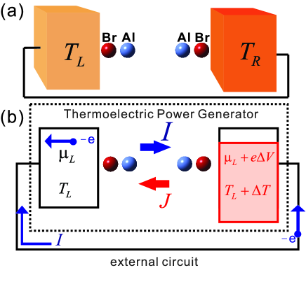
Thermoelectric power generators in bulk systems employ electron gas as a working fluid. It directly converts thermal energy into electric energy using the Seebeck effect. Provided a temperature difference is maintained across the device, it can generate electric power converted from the thermal energy. In this paper, we explore the energy conversion mechanism of nanojunctions. We present a parameter-free first-principles calculations for a thermoelectric power generator in a truly atomic-scale system. To gain further insight into the mechanism of energy conversion, we also developed an analytical theory for it. As a specific example, we consider an atomic junction depicted in Fig. 1(a), where the left and right electrodes serve as independent cold- and hot-temperature reservoirs, respectively. This is not just an academic example since recent studies have demonstrated the capability to assemble one magnetic atom on a thin layer of atoms on the surface of STM Heinrich . A similar technique might be applicable to a single Al atom adsorbed onto a layer of Br atoms on the metal surface. In this regard, the atomic junction could be formed by bringing two identical pieces of metal-Br-Al surfaces close together before the reconstruction of Br and Al atoms occurs.
As it was found in Ref. 57, the paired metal-Br-Al junction shows interesting device properties, such as negative differential resistance, that utilize the relatively narrow density of states (DOSs) near the chemical potentials. The narrow DOSs are due to the weak coupling between the Al atoms and the electrodes via the “spacer” Br atoms Lyo ; Lang3 . This junction also serves as an efficient field-effect transistor because the narrow DOSs near chemical potentials can be easily shifted by the gate voltages. As the Seebeck coefficients are relevant to the slope of DOSs, the sharp DOSs result in a large magnitude in the Seebeck coefficient Liu . When a temperature difference is maintained between electrodes in a closed circuit, the Seebeck effect generates an electromotive force (), which drives a current flowing through the junction, hence the nanojunction can also be considered as an efficient thermoelectric power generator Justin .
We investigate further the possibility of powering an atomic-scale device as a field-effect transistor using heat instead of electricity. To illustrate this point, we consider the paired metal-Br-Al junction in a three-terminal geometry. When a finite temperature difference is maintained between electrodes, the Seebeck effect converts the electron’s thermal current into the electric current flowing through the nanojunction. We observe that the current’s magnitude, polarity, and power on-off are controllable by the gate field. Such current-voltage characteristics could be useful in the design of nanoscale electronic devices, such as a transistor or switch.The nanojunction, therefore, can be considered a transistor that employs the Seebeck effect to power itself by converting the thermal energy into electric energy. The results of this study may be of interest to researchers attempting to develop new styles of thermoelectric nano-devices.
The flow of the discussion in this paper is as follows. In Sec. II, we describe density functional theory, theory of thermoelectricity, and theory of thermoelectric power generator as a self-powered electronic device. In Sec. III, we discuss the thermoelectric properties of nanojunctions and the thermoelectric power generator as a self-powered device. Finally, we conclude our findings in Sec. IV.
II Theoretical Methods
We briefly present an introduction of the Lippmann-Schwinger (LS) equation and density-functional theory (DFT) in subsection A. In subsection B, we present the theory of the Seebeck coefficient, electric conductance and thermal conductance. In subsection C, we present the theory to calculate the Seebeck-induced electric current, voltage, power, and efficiency of energy conversion. These quantities are calculated in the truly atomic scale junction in terms of the nonequilibrium scattering wave-functions obtained self-consistently in the framework of DFT+LS calculations. Both DFT+LS and DFT+Keldysh nonequilibrium Green’s function (NEGF) have been applied extensively to a wide range of problems of nonequilibrium quantum transport of device physics problems under finite biases from first-principles approaches. The formal connection between DFT+LS and DFT+NEGF can be found in Ref. 61.
II.1 Density Functional Theory and Lippmann-Schwinger Equation
We model a nanoscale junction as a passive element formed by two semi-infinite metal with planar surfaces held a fixed distance apart connecting to an external battery of bias , with a nano-structured object bridging the gap between them. The full Hamiltonian of the system is , where is the Hamiltonian due to the biased bimetallic electrodes that we model as ideal metal (jellium model), and is the scattering potential of a group of atoms bridging the gap. We assume that the left electrode is positively biased such that , where and are the chemical potential deep in the left and right electrodes, respectively.
The unperturbed wave functions of the biased bimetallic electrodes have the form, , where is the coordinate parallel to the surfaces and is the coordinate normal to them. Electrons are free to move in the plane perpendicular to the direction, and is the momentum of electron in the plane parallel to the electrode surfaces. Partial charges spilled from the electrode positive-background edges into the vacuum region. This causes an electrostatic potential barrier between two electrodes. The charge density distribution and effective single-particle wave functions are calculated in the framework of the density functional formalism by solving the coupled Shrödinger and Poisson equations iteratively until self-consistency is obtained Lang4 . The wave function describes the electrons incident from the right electrode, satisfying the following boundary condition :
| (1) |
The group of atoms is considered in the scattering approaches. Corresponding to each of the unperturbed wave functions, a Lippmann-Schwinger equation involving a Green’s function for the biased bimetallic junction is solved in the plane wave basis, where a basis of approximately plane waves has been chosen for this study Lang :
| (2) |
where represents the nonequilibrium scattering wave function of the electrons with energy incident from the left (right) electrode. The quantity is the Green’s function for the biased bimetallic electrodes and is the scattering potential electrons experience:
| (3) |
where is the electron-ion interaction potential represented with pseudopotential; is the exchange-correlation potential calculated at the level of the local-density approximation; is the electron density for the pair of biased bare electrodes; is the electron density for the total system; and is their difference. The wave functions of the entire system are calculated iteratively until self-consistency is obtained Lang .
These right- and left-moving wave functions, weighed with the Fermi-Dirac distribution function according to their energies and temperatures, are applied to calculate the electric current as:
| (4) |
where and represents an element of the electrode surface. Here, we assume that the left and right electrodes are independent electron reservoirs, with the electron population described by the Fermi-Dirac distribution function, , where and are the chemical potential and the temperature in the left (right) electrode, respectively. More detailed descriptions of theory can be found in Refs. 63; 5; 64.
The above expression can be cast in a Landauer-Büttiker formalism:
| (5) |
where is a direct consequence of the time-reversal symmetry, and is the transmission function of the electron with energy incident from the right (left) electrode,
| (6) |
Note that is positive in the definition of Eq. (5).
The electron’s thermal current, defined as the rate at which thermal energy flows from the right (into the left) electrode, is
| (7) |
respectively.
II.2 Theory of the Thermoelectric Properties in the Nanoscale Junctions
We assume that the nanojunction is not connected to external circuit such that and , and then we consider an infinitesimal current [ induce by an infinitesimal temperature difference raised in the right electrode [i.e., ]. The Seebeck effect generates a voltage difference in the right electrode [i.e., ] which drives current []. The current cannot actually flow, thus, counterbalances [i.e., ]. The Seebeck coefficient (defined as ) can be obtained by expanding the Fermi-Dirac distribution functions in and to the first order in and :
| (8) |
where
| (9) |
The Seebeck coefficient up to the lowest order in temperatures is,
| (10) |
where Liu2 . Here, we have expanded to the lowest order in temperatures by using Sommerfeld expansion: , , and . The Seebeck coefficient is positive (negative) when the slope of transmission function is negative (positive) near the chemical potential.
When a finite temperature difference is raised in the right electrode, the Seebeck effect generates a finite electromotive force, , raising the potential energy of the charge. We assume that the voltage difference is applied to the right electrode such that and . The voltage difference generated by the temperature difference is approximately given by,
| (11) |
where the Seebeck coefficient is given by Eq. (8) with . Equation (11) becomes exact when . The sign of depends on the sign of the Seebeck coefficient . For example, for , as shown in Fig. 1(b).
Equation (11) is an approximation when is finite. We have to remind ourselves of the fact that the left chemical potential differs from the right chemical potential when the temperature difference is large. In this case, the Seebeck coefficient becomes relevant to both and with a more complicated form Liu ,
| (12) |
where and are given by Eq. (9). A more elaborate evaluation of the voltage difference can be performed using,
| (13) |
where , and .
The induced voltage by the Seebeck effect using Eq. (11) and (13) have been numerically verified, showing that Eq. (11) is a good approximation when the transmission function does not change rapidly around the chemical potentials and when is not too large. Accordingly, we evaluate throughout this study using Eq. (11) instead of Eq. (13) for simplicity.
Corresponding to the electric current, the extra electron’s thermal current induced by an infinitesimal temperature () and voltage () across the junctions is,
| (14) |
where and can be calculated by Eq. (7).
The electron’s thermal conductance (defined as ) can be decomposed into two components:
| (15) |
where and . Using Sommerfeld expansion, they can be can be written as,
| (16) |
and
| (17) |
where and are given by Eq. (9). One should note that if the Seebeck coefficient of the system is zero.
By expanding and to the lowest order in temperatures, Eqs. (16) and (17) become
| (18) |
where and . In the above expansions, we have applied the Sommerfeld expansions: , , and Eq. (10).
In the limit of zero bias, Eq. (5) yields the electric conductance (defined as ),
| (19) |
which is relatively insensitive to temperatures if tunneling is the major transport mechanism.
II.3 Theory of the Thermoelectric Power Generator as a Self-powered Electronic Device
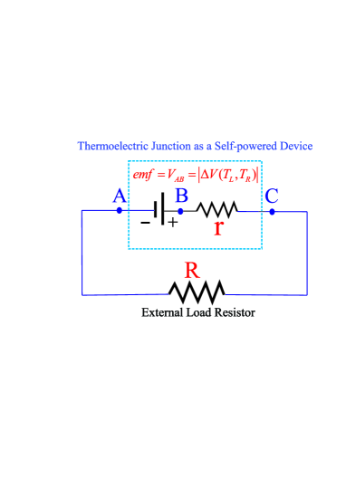
In this subsection, we present a closed-circuit theory of the thermoelectric nanojunction as a power generator and a self-powered electronic device by itself. We consider the nanojunction with the Seebeck coefficient and such that the open-circuit Seebeck-effect induced is , as depicted in Fig. 1(b). Figure 1(b) can be represented as a circuit diagram shown in Fig. 2, where the thermoelectric junction is considered to consist an ideal battery of plus an internal resistance . The thermoelectric junction employs the Seebeck effect to generate an and converts thermal energy into electric energy. Concurrently, the nanojunction itself serves as a passive element with resistance which consumes electric energy.
We choose clockwise as positive such that the induced current for . Beginning at point as the current traverses the circuit in the positive direction, we obtain from Kirchhoff’s loop rule,
| (20) |
where the open-circuit is for , is the internal resistance of the nanojunction, and is the resistance of the external resistor, as depicted in Fig. 2. Note that the current encounters a potential increase due to the source of between points and , a potential drop [] due to the internal resistance between points and , and a potential drop [] as the current traverses the external resistor with resistance between points and , respectively.
In particular, we carry out this research considering such that the voltage drop between points and is . It yields
| (21) |
It implies that external circuit does not consume electric energy because the potential difference across two terminals of the thermoelectric power generators (i.e., the terminal voltage) is zero due to . This simplified scenario helps us to analyze the detailed mechanism of energy conversion between the thermal current and electric current. Such analysis will provide us an insight into the device physics of the thermoelectric junctions as self-powered electronic devices.
The current can be evaluated by Eq. (21), where is the Seebeck-effect induced [which is evaluated by Eq. (12)] and is the conductance of nanojunction [which is evaluated by Eq. (19)]. We have numerically verified and confirmed that , where
| (22) |
and
| (23) |
The above two equations have the sign convention conformed to the direction of current depicted Fig. 1(b) and Fig. 3 for . We may interpret as the current which traverses the thermoelectric nanojunction as a ”pure” source of generated by the temperature difference using the Seebeck effect. Similarly, is the current which traverses the nanojunction as an internal resistor. Equations (22) and (23) describe the flow of electrons associated with the probability flux.
The flow of probability density can also transport energy as electrons travel between two electrodes. The electrons that travel with energy from the right (left) electrode carry an amount of energy . Correspondingly, the -induced energy current carried by the probability current flowing out of the right electrode (into to the left electrode) is,
| (24) |
where and is given by Eq. (11). Similarly, the -induced electron’s thermal current carried by the probability current flowing out of the right electrode (into to the left electrode) is,
| (25) |
Note that and are positive and for . The sign convention defined in Eqs. (22)-(25) comply with the direction depicted in Fig. 1(b) and Fig. 2 for .
Subtracting from , we obtain
| (26) |
where is the electric power delivered by the thermoelectric junction served as a ”pure” battery which employs the Seebeck effect to convert the electron’s thermal current into electric energy. If the external resistor with resistance , then the external circuit does not consume electric energy. In this case, the nanojunction simultaneously serves as an electronic device which consumes the entire electric power generated by itself,
| (27) |
Note that Eq. (27) can alternatively be expressed as,
| (28) |
Eqs. (26)-(28) have been numerically verified to be consistent with each other. If the system is n-type (i.e., ), then and , as shown in Fig. 1(b). Similarly, if the system is p-type (i.e., ), then and . Both cases render .
III Results and Discussion
Provided that a finite temperature difference is raised between electrodes, the Seebeck effect will generate an electric current. It is observed that the nanojunction itself can be deemed a field-effect transistor, where gate field can control the current. Thus and so, the atomic junction in three-terminal geometry can be considered as an electronic device which can be self-powered by providing a temperature difference across the junction.
As an a specific example, we consider an atomic-scale junction in a three-terminal geometry as a thermoelectric power generator, depicted in Fig. 6(a). In the paired metal-Br-Al junction, we assume that the distance between two Al atoms is sufficiently large. The interaction between two pieces of metal-Br-Al is minimal, and in this fashion, no rearrangement of atom positions occurs. Accordingly, the phonon’s thermal current could be suppressed because of poor mechanical coupling between two pieces of metal-Br-Al is minimal. We neglect it for simplicity in this study.
III.1 Thermoelectric Properties of the Junction
In an open circuit, an infinitesimal temperature raised in the right electrode induces and which counterbalance each other. This renders the Seebeck coefficient defined in Eq. (8), as described in subsection IIB.
Correspondingly, the electron’s thermal conductance is defined as , as given by Eq. (15). The electron’s thermal conductance can be decomposed into two components, , where and are given by Eqs. (16) and (17), respectively.
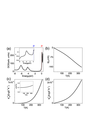
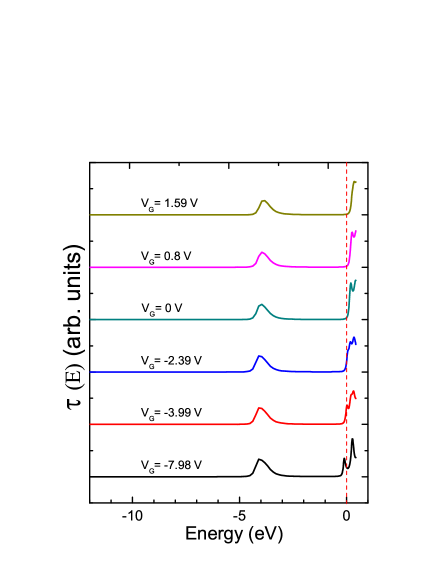
Fig. 3(a) shows that the system is characterized by a sharp transmission function corresponding to a narrow DOSs near the chemical potential. As it was found in Ref. 57, the DOSs become narrower when the distance between two Al atoms increases. The narrow DOSs result in substantial Seebeck coefficients, as shown in Fig. 3(b). It shows that the thermoelectric junction is n-type () since the narrow DOSs are slightly above the chemical potential and the slope of the transmission is positive. At low temperatures (about K), the Seebeck coefficients remain linear (), as described in Eq. (10). We present the absolute values of and as functions of temperatures in Fig. 3(c) and (d), respectively. At low temperatures, and , as shown in Eq. (18). The inset of Fig. 3(c) shows the zero-bias electric conductance as a function of temperatures calculated from Eq. (19).
III.2 The Junction as a Thermoelectric Power Generator and a Self-powered Electronic Device
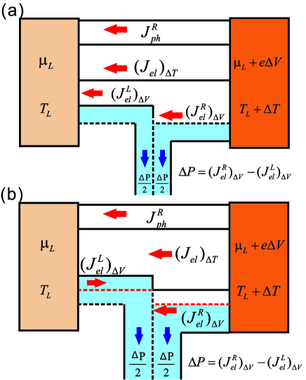
Suppose that the junction is not connected to battery (i.e., ) and . Provided that a finite temperature difference is raised in the right electrode (i.e., and ), the Seebeck effect generates a finite electromotive force , where is given by Eq. (11). This voltage difference induces a net electric current which travels from lower to higher potential inside the power generator, as described in Eq. (22) and Fig. 1(b). Correspondingly, the electron’s thermal current [Eq. (24)] absorbs energy in heat from the hot (right) electrode, produces electric power [Eq. (26)] using the Seebeck effect, and then gives up energy in heat to the cold (left) electrode via [Eq. (24)], as described in Fig. 1(b) for .
To gain further insight into the mechanism of energy conversion, we theoretically analyze the electron’s thermal current. Applying Sommerfeld expansion to and in Eq. (24), we obtain
| (29) |
and
| (30) |
where we have simplified Eqs. (29) and (30) using the following approximations: , , , , and .
Equations. (29) and (30) immediately provides the law of energy conservation as further described below. The thermoelectric junction serves as an ideal source of which delivers electric power converted from the electron’s thermal currents using the Seebeck effect. Concurrently, the nanojunction itself serves as a passive element which consumes electric power dissipated by the internal resistor at a rate of .
Equations (29) and (30) imply that each electrode approximately provides one half of the electric power using the Seebeck effect and the electric power is mainly converted from . No energy conversion is possible when the Seebeck coefficients is vanishing because . We note that removes heat energy from the hot electrode, converts heat energy into electric energy, and rejects waste heat to the cold electrode by . Both and do not play active role in the energy conversion. The above discussions are summarized in Fig. 4(a).
The energy current flowing into the cold electrode could be negative when is sufficiently large, as shown in Fig. 4(b). To show this, we integrate Eq. (11) using Eq. (10), , . We obtain , where . Together with Eq. (30), we arrive at
| (31) |
from which we observe that changes sign at (which is universal), and when . Fig. 4(a) and 4(b) illustrate the schematic representation of energy conversion for positive and negative , respectively. Fig. 4(a) and 4(b) illustrate the schematic representation of energy conversion for positive and negative , respectively.
Let us focus on the energy conversion efficiency defined as the ratio of the electric power generated by the Seebeck effect to the electron’s thermal current which removes thermal energy from the high temperature reservoir:
| (32) |
where , , and are given by Eq. (28), (24), and (25), respectively. In the above definition, we have neglect other effects [e.g. the phonon’s thermal current and possible photon radiation] which transfer energy from the hot to cold electrodes. From this viewpoint, the energy conversion efficiency presented in this study may be overestimated. We note that the size of the paired metal-Br-Al system is small. This may lead to suppression of the photon radiation because photon radiation is proportional the surface area. Moreover, the paired metal-Br-Al system has a poor mechanical link between electrodes when the distance of two Al atoms is sufficiently far apart. The poor mechanical coupling between two phonon reservoir could lead to suppression of the phonon’s thermal current. These two features are helpful to increase the energy conversion efficiency. Note that the phonon’s thermal current and photon radiation do not affect the magnitudes of the current and electric power generated by the Seebeck effect.
To show that the atomic junction can be considered as a field-effect transistor which can be self-powered, we consider the nanojunction in a three-terminal geometry with a finite temperature K maintained between electrodes (where K and K). The gate field is introduced as a capacitor composed of two parallel circular charged disks separated at a certain distance from each other. The axis of the capacitor is perpendicular to the transport direction. One plate is placed close to the nano-object while the other plate, placed far away from the nano-object, is set to be the zero reference field DiVentragate ; Solomon1 ; Solomon2 ; Ma .
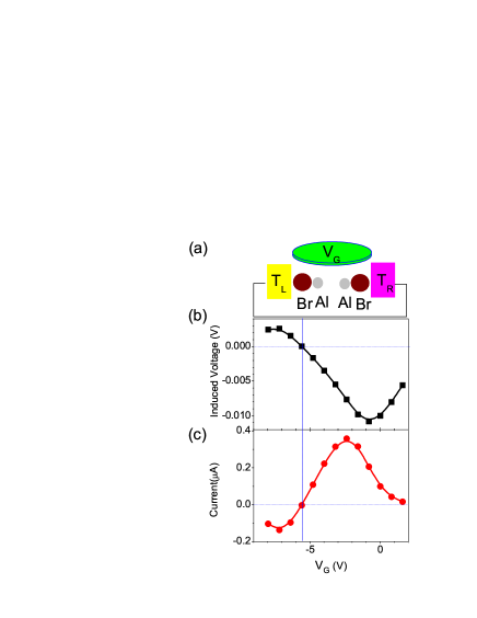
The nanojunction can be considered as a field-effect transistor which is powered by itself via the temperature difference maintained between electrodes using the Seebeck effect. We observe that the gate voltages can shift the narrow DOSs and transmission function near the chemical potential, as shown in Fig. 5. Figure 6 shows the induced potential [upper panel; given by Eq. (11)] and current [lower panel; given by Eq. (22)] for K and K as functions of gate voltages. We observe that the extremal of and do not occurs at the same value of because the gate voltage also modulates the conductance of the junction [note that ]. Figure 6 demonstrates that the gate field can efficiently control the magnitude, polarity, and power on-off of the voltage and current induced by the Seebeck effect. Such current-voltage characteristics could be useful in the design of nanoscale electronic devices such as a transistor or switch. Note that the induced voltage and induced current described in Fig. 6 comply with the sign convention described in Fig. 1(b).
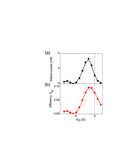
Figure 7 shows the electric power [upper panel; given by Eq. (26)] delivered by the battery and the energy conversion efficiency [lower panel; given by Eq. (32)] as functions of the gate voltages. It illustrates that the gate field is capable of controlling and optimizing the electric power and energy conversion efficiency . The energy conversion efficiency if optimized by the gate field. The optimized power is about nW at V. We also observe that the maximum values of electric power and energy conversion efficiency occur at different voltages, similar to the case of induced voltage and current. If a macroscopic system can be formed by two identical pieces of surfaces, each of which is formed by a layer of Al atoms adsorbing onto metal surface coated with a layer of Br atoms as spacer. The macroscopic system could be equivalent to more than single paired metal-Br-Al-Al-Br-M junctions which are connected in parallel on cm2 surface. We conjecture that the power could be substantial in such a macroscopic system.
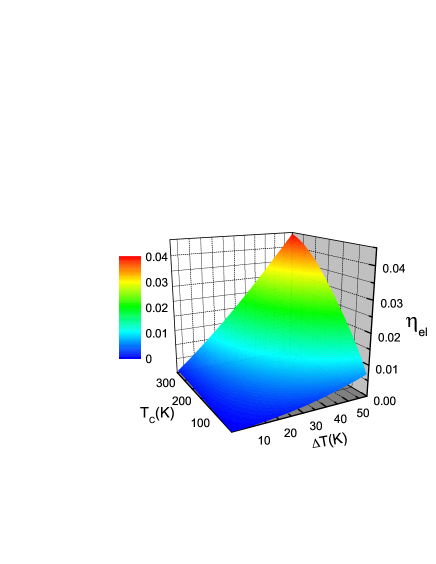
Finally, we investigate the efficiency of energy conversion as a function of () and for , as shown in Fig. 8. The paired metal-Br-Al junction shows sufficiently large efficiency around when K and K. Such a high efficiency is attributed to the enhanced the Seebeck coefficients.
IV Conclusions
In summary, we developed a theory for thermoelectric power generator in the truly atomic scale system. The theory is general to any atomic/molecular junction where electron tunneling is the major transport mechanism. As an example, we investigated the thermoelectric properties and the efficiency of energy conversion of the paired metal-Br-Al junction from first-principles approaches. Owing to the narrow states near the chemical potentials, the nanojunction has large Seebeck coefficients; thus, it can be considered as an efficient thermoelectric power generator. Provided that a finite temperature difference is maintained between electrodes, the thermoelectric power generator converts thermal energy into electric energy. The optimized electric power generated by the Seebeck effect is about nW at K at V. To gain further insight into the mechanism of energy conversion, we investigate the electron’s thermal currents analytically. The electron’s thermal current which removes heat from the hot temperature reservoir can be decomposed into two components, . Only is capable of converting energies. The electron’s thermal current removes heat from the hot reservoir via and rejects waste heat into the cold reservoir via . No energy conversion is possible when the Seebeck coefficients is vanishing.
We also consider the nanojunction in a three-terminal geometry, where the current, voltage, and electric power can be modulated by the gate voltages, which shift the states of the junction. We observe that the gate field can control the magnitude, power on-off, and polarity of the induced current and voltages generated by the Seebeck effect. Such current-voltage characteristics could be useful in the design of nanoscale electronic devices such as a transistor or switch. Notably, the nanojunction as a transistor with a fixed finite temperature difference between electrodes can power itself using the Seebeck effect. The results of this study may be of interest to researchers attempting to develop new forms of thermoelectric nano-devices.
The authors thank Ministry of Education, Aiming for Top University Plan (MOE ATU), National Center for Theoretical Sciences (South), and National Science Council (Taiwan) for support under Grants NSC 97-2112-M-009-011-MY3, 098-2811-M-009-021, and 97-2120-M-009-005.
References
- (1) A. Aviram and M. A. Ratner, Chem. Phys. Lett. 29, 277 (1974).
- (2) M. A. Reed, C. Zhou, C. J. Muller, T. P. Burgin, and J. M. Tour, Science 278, 252 (1997).
- (3) M. Di Ventra, Electrical transport in nanoscale systems, (Cambridge University Press, Cambridge, 2008).
- (4) C. C. Kaun and H. Guo, Nano Lett. 3, 1521 (2003).
- (5) M. Di Ventra and N. D. Lang, Phys. Rev. B 65, 045402 (2001).
- (6) A. Nitzan and M. A. Ratner, Science 300, 1384 (2003).
- (7) W. Wang, T. Lee, I. Kretzschmar, and M. A. Read, Nano Lett. 4, 643 (2004).
- (8) M. Galperin, A. Nitzan, and M. A. Ratner, Phys. Rev. B 78, 125320 (2008).
- (9) J. Jiang, M. Kula, W. Lu, and Y. Luo, Nano Lett. 5, 1551 (2005).
- (10) L. H. Yu, C. D Zangmeister, and J. G. Kushmerick, Phys. Rev. Lett. 98, 206803 (2007).
- (11) M. Paulsson, T. Frederiksen, and M. Brandbyge, Nano Lett. 6, 258 (2006).
- (12) G. C. Slomon, A. Gagliardi, A. Pecchia, T. Frauenheim, A. Di Carlo, J. R. Reimers, and N. S. Noel, J. Chem. Phys. 124, 094704 (2006).
- (13) J. G. Kushmerick and J. Lazorcik, C. H. Patterson, and R. Shashidhar, Nano Lett. 4, 639 (2004).
- (14) Y. C. Chen, M. Zwolak, and M. Di Ventra, Nano Lett. 5, 621 (2005).
- (15) Y. C. Chen, Phys. Rev. B 78, 233310 (2008).
- (16) I. S. Kristensen, M. Paulsson, K. S. Thygesen, and K. W. Jacobsen, Phys. Rev. B 79, 235411 (2009).
- (17) D. Djukic and J. M. van Ruitenbeek, Nano Lett. 6, 789 (2006).
- (18) M. Kiguchi, O. Tal, S. Wohlthat, F. Pauly, M. Krieger, D. Djukic, J. C. Cuevas, and J. M. van Ruitenbeek, Phys. Rev. Lett. 101, 046801 (2008).
- (19) P. J. Wheeler, J. N. Russom, K. Evans, N. S. King, and D. Natelson, Nano Lett. 10, 1287 (2010).
- (20) Y. C. Chen and M. Di Ventra, Phys. Rev. Lett. 95, 166802 (2005).
- (21) Y. S. Liu and Y. C. Chen, Phys. Rev. B 83, 035401 (2011).
- (22) Y. C. Chen, M. Zwolak, and M. Di Ventra, Nano Lett. 3, 1691 (2003).
- (23) Z. Huang, B. Xu, Y. C. Chen, M. Di Ventra, and N. J. Tao, Nano Lett. 6, 1240 (2006).
- (24) M. Di Ventra, S. T. Pantelides, and N. D. Lang, Appl. Phys. Lett. 76, 3448 (2000).
- (25) C. L. Ma, D. Nghiem, and Y. C. Chen, Appl. Phys. Lett. 93, 222111 (2008).
- (26) P. M. Solomon and N. D. Lang, ACS Nano 2, 435 (2008).
- (27) N. D. Lang and P. M. Solomon, ACS Nano 3, 1437 (2009).
- (28) H. Song, Y. Kim, Y. H. Jang, H. Jeong, M. A. Reed, and T. Lee, Nature 462, 1039 (2009).
- (29) C. H. Ahn, A. Bhattacharya, M. Di Ventra, J. N. Eckstein, C. D. Frisbie, M. E. Gershenson, A. M. Goldman, I. H. Inoue, J. Mannhart, A. J. Millis, A. F. Morpurgo, D. Natelson, and J. M. Triscone, Rev. Mod. Phys. 78, 1185 (2006).
- (30) S. M. Lindsay and M. A.Ratner, Advanced Materials 19, 23 (2007).
- (31) N. J. Tao, Nat. Nanotechnol. 1, 173 (2006).
- (32) B. Ludoph and J. M. van Ruitenbeek, Phys. Rev. B 59, 12290 (1999).
- (33) P. Reddy, S. Y. Jang, R. A. Segalman, and A. Majumdar, Science 315, 1568 (2007).
- (34) K. Baheti, J. A. Malen, P. Doak, P. Reddy, S. Y. Jang, T. D. Tilley, A. Majumdar, and R. A. Segalman, Nano Lett. 8, 715 (2008).
- (35) J. A. Malen, P. Doak, K. Baheti, T. D. Tilley, R. A. Segalman, and A. Majumdar, Nano Lett. 9, 1164 (2009).
- (36) J. A. Malen, S. K. Yee, A. Majumdar,and R. A. Swgalman, Chem. Phys. Lett. 491, 109 (2010).
- (37) M. Paulsson and S. Datta, Phys. Rev. B 67, 241403(R) (2003).
- (38) X. Zheng, W. Zheng, Y. Wei, Z. Zeng, and J. Wang, J. Chem. Phys. 121, 8537 (2004).
- (39) B. Wang, Y. Xing, L. Wan, Y. Wei, and J. Wang, Phys. Rev. B 71, 233406 (2005).
- (40) F. Pauly, J. K. Viljas, and J. C. Cuevas, Phys. Rev. B 78, 035315 (2008).
- (41) Y. Dubi and M. Di Ventra, Nano Lett. 9, 97 (2009).
- (42) T. Markussen, A. P. Jauho , and M. Brandbyge, Phys. Rev. Lett. 103, 055502 (2009).
- (43) S. H. Ke, W. Yang, S. Curtarolo, and H. U. Baranger, Nano Lett. 9, 1011 (2009).
- (44) C. M. Finch, V. M. García-Suárez, and C. J. Lambert, Phys. Rev. B, 79, 033405 (2009).
- (45) T. Markussen, A. P. Jauho, and M. Brandbyge, Phys. Rev. B, 79, 035415 (2009).
- (46) J. P. Bergfield and C. A. Stafford, Nano Lett. 9, 3072 (2009).
- (47) Y. S. Liu, Y. R. Chen, and Y. C. Chen, ACS Nano 3, 3497 (2009).
- (48) M. Galperin, A. Nitzan, and M. A. Ratner, Molecular Phys. 106, 397 (2008).
- (49) O. Entin-Wohlman, Y. Imry, and A. Aharony, Phys. Rev. B 82, 115314 (2010).
- (50) B. C. Hsu, Y. S. Liu, S. H. Lin, and Y. C. Chen, Phys. Rev. B (in press).
- (51) M. Esposito, K. Lindenberg and C. Van den Broeck, Phys. Rev. Lett. 102, 130602 (2009).
- (52) Y. S. Liu and Y. C. Chen, Phys. Rev. B 79, 193101 (2009).
- (53) Y. Dubi and M. Di Ventra, Phys. Rev. B 79, 081302(R) (2009).
- (54) M. Galperin, K. Saito, A. V. Balatsky, and A. Nitzan, Phys. Rev. B 80, 115427 (2009).
- (55) Y. S. Liu, B. C. Hsu, and Y. C. Chen, cond-mat/arXiv:0908.0992.
- (56) C. F. Hirjibehedin, C. P. Lutz, and A. J. Heinrich, Science 312, 1021 (2006).
- (57) N. D. Lang, Phys. Rev. B 55, 9364 (1997).
- (58) I. M. Lyo, Ph. Avouris, Science 245, 1369 (1989).
- (59) M. L. Yu, N. D. Lang, B. W. Hussey, T. H. P. Chang, and W. A. Mackie, Phys. Rev. Lett. 77, 1636 (1996).
- (60) J. P. Bergfield, M. A. Solis, and C. A. Stafford, ACS Nano 4, 5314 (2010).
- (61) J. Wang and H. Guo, Phys. Rev. B, 79, 045119 (2009).
- (62) N. D. Lang, Phys. Rev. B, 45, 13599 (1992).
- (63) N. D. Lang, Phys. Rev. B 52, 5335 (1995).
- (64) Y. C. Chen and M. Di Ventra, Phys. Rev. B 67,153304 (2003).