Electronic correlations and disorder in transport through one-dimensional nanoparticle arrays
Abstract
We analyze and clarify the transport properties of a one-dimensional metallic nanoparticle array with interaction between charges restricted to charges placed in the same conductor. We study the threshold voltage, the I-V curves and the potential drop through the array and their dependence on the array parameters including the effect of charge and resistance disorder. We show that very close to threshold the current depends linearly on voltage with a slope independent on the array size. At intermediate bias voltages, for which a Coulomb staircase is observed we find that the average potential drop through the array oscillates with position. At higher voltages I-V curves are linear but have a finite offset voltage. We show that the slope is given by the inverse of the resistances added in series and estimate the voltage at which this linear regime is reached. We also calculate the offset voltage and relate it to the potential drop through the array.
pacs:
73.23-b,73.63.-b,73.23.HkNanoparticle arrays made of metallicmetallicwhetten ; metallicheath ; metallicjaegerdis ; metallickiehl ; metalliclin ; metallicjaegerquasi1d ; metalliczhang ; metallicjaegernature ; metallicschoenen ; metallicysemi , semiconductingmetallicysemi ; semimurray ; semitalapin ; semibawendi ; semisionnest ; semidrndic ; semiheath , magneticmagneticsun ; magneticblack ; magneticpuntes or combinedmixedredl ; mixedkorgel ; mixedshevchenko materials and with radii of the order of 2-7 nm can be now synthesized. The transport properties of these systems are influenced by the ratio between the energy level spacing, the charging energy of the nanoparticles, and the temperature. The first two quantities depend on the material and the size of the nanoparticle. In the case of metallic nanoparticles, at not too low temperatures, the level spacing is much smaller than the temperature and does not play any role in the transportsinglecharge . On the contrary, the charging energy is of the order of 0.1 eV. Strong interactions between the electric charges and the possibility of tuning interparticle coupling make nanoparticles arrays an ideal system to study correlated motioncollectiveheath1 ; collectiveheath2 ; collectiveheathpb ; collectivebard ; collectivekorgel ; collectivepileni ; collectivesheng ; Middleton93 ; Matsuoka98 ; Shin98 ; Kaplan02 ; Kaplan03 ; Kinkhabwala04 ; DasSarma ; Belobodorov ; Glazman ; Turlakov ; Efetov ; Shklovskii .
Experimentally, these arrays are strongly influenced by disorderdisorderjaeger ; disorderheath ; disordercordan . Local charging disorder is present in all arrays due to randomly dispersed charged impurities lodged in the substrate or in the materials that separate and surround the nanoparticles. Because of the exponential dependence of the tunneling resistance, even a small dispersion in the distance between nanoparticles results in large variations in the tunneling resistances of the junctions. Differences in the island sizes and voids in the lattice can be other sources of disordermetallicjaegerdis .
Due to the combination of disorder and charging effects the current in voltage biased arrays is blocked up to a threshold voltagedisorderjaeger ; Tinkham99 ; Ancona01 ; Bakhalov89 ; Middleton93 ; Hu94 ; Melsen97 ; Berven01 ; Kaplan03 ; Schoeller05 . For bias voltages larger than current is in general non-linear in voltage with a power-law dependencedisorderjaeger ; Tinkham99 ; Clarke98 close to threshold, a linear dependence recovered at high-voltages and frequently a step-like behavior, called a Coulomb staircase, at intermediate voltages. Most studies have focused on the statistical analysis of the threshold voltage and on the power-law behavior of the current close to this threshold. This exponent depends on the dimensionality of the array, but there is controversy between different theoretical approaches in the one-dimensional case, with both linearMiddleton93 ; Kaplan03 ; Jha05 and square-rootReichhardt03 predictions. Much experimental work has been concentrated on two and three dimensional arrays, but some quasi-one dimensional systems have also been fabricatedmetallickiehl ; metallicjaegerquasi1d ; Tinkham99 . Comparison between experiments and theory is not yet well settled.
In this paper we provide a complete description of the zero-temperature transport properties of one-dimensional metallic nanoparticle arrays for the case in which interactions are restricted to charges in the same nanoparticle (onsite limit). In a separate workpaperlongrange we discuss the effect of the long-range character of the interactions on these properties. We resolve the controversy on the power-law, analyze carefully dependencies on different array parameters and estimate the voltage which delimits each of the transport regimes to favor comparison with experiment. We discuss arrays with and without charge disorder. Although clean arrays are mainly of academic interest, their analysis will help us to understand the main features of the experimentally more relevant, disordered arrays. The effect of variations in the junction resistances is also analyzed. Disorder in capacitances (nanoparticle size variations) is not considered as it is less important in present experiments. Nanoparticles synthesized nowadays are monodispersed in size to a few percent. In any case, the effect of capacitance disordercap in most of the properties studied here can be deduced from the analytic approximations provided in the text. Due to the one-dimensionality of the array and the nearest neighbor tunneling considered we assume that there are no nanoparticle voids in the array, as this would completely prevent current flow. We have analyzed the threshold voltage, the I-V characteristics, close to threshold but also at larger bias voltages and the potential drop through the array. Among the results presented we show that the threshold voltage of clean arrays in the onsite case does not approach the one found for capacitively coupled junctions in the limit of weak couplingBakhalov89 ; Hu94 . The controversy in the power-law dependence of current on bias voltage close to threshold is clarified and shown to be linear, but with a slope different from the one previously predictedJha05 . We find signatures of correlated charging of the system in the potential drop through the array, especially at intermediate values of the bias voltage. We show that even at high voltages, with the conductance controlled by the sum of the resistances in series, the potential drop through the array is not completely linear, but it has a contribution due to charging effects. We identify an asymmetry external parameter which controls the bias voltage drop. The influence of has barely been discussed in previous works. We show that its effect can a priori be observed experimentally in the width of the Coulomb staircase steps. Calculations are perfomed numerically, but analytic approximations are given in several limits and compared with numerical results.
I THE MODEL
We analyze the current through a one-dimensional array of metallic nanoparticles placed between two electrodes. We consider the classical Coulomb blockade regime with . is the level spacing, the temperature and the charging energy of the islands, with capacitance . Here and in the following the electronic charge We assume that each nanoparticle has a continuum level spectrum () and a constant density of states at the Fermi level, but a gap for adding charge. We restrict electrostatic interactions to those charges on the same conductor: capacitive coupling vanishes. This limit is referred to as short-range or onsite interaction limit. The nanoparticles are separated by high tunneling barriers with a resistance much larger than the quantum of resistance. In these conditions the charge in the islands can be assumed fixed and quantized. Eventually we allow tunneling processes between nearest neighbors, and treat the transport at the sequential tunneling level. A single charge is involved in the tunneling process. We assume that when a charge hops, the charge density in the final state of the array immediately relaxes to the electrostatic equilibrium configuration.
We take into account that the electrodes are not ideal voltage sources, but have a finite self-capacitance. In equilibrium, and before the tunneling event the electrodes are held at a given potential due to the charge provided by a battery. We assume that the tunneling time, i.e. the time needed by the electron to cross the tunnel barrier, is smaller than the circuit characteristic time that determines how quickly the battery can transfer charge to the leads in order to restore the voltage at the electrodes. As a consequence, just after the tunneling process the electrodes will not necessarily be at the same potential at which they were at before the tunneling event because the charge, provided by the battery, necessary to restore their initial potentials has not arrived yet. The voltage is restored to the nominal value before the next tunneling event. For finite-range interactions the potentials on the leads will thus fluctuate in response to all tunneling events, even those that do not directly involve the electrodes. In the short-range case, considered here, they will fluctuate only when an electron jumps into or out of the leads.
The current is calculated numerically by means of a Monte Carlo simulation, described in the Appendix, which depends on the tunneling rates. The probability of a tunneling processsinglecharge is given by
| (1) |
with the tunneling resistance of the junction. We will restrict the discussion to zero temperature for which . is the difference between the energy of the system before and after the tunneling event, with the sign convention that is negative if the energy decreases. It excludes the work done by the battery to recharge the electrodes, as explained before. The energy gained by tunneling is assumed to be dissipated. Only changes in energy with electrostatic origin are considered. The energy of our system is given by
| (2) |
Labels and refer to source and drain electrodes and ,…, to the islands. In the following, latin capital and lower case letters are used to denote electrodes and islands respectively. Greek indexes will be used when the labels refer to both islands and electrodes. and are respectively the conductor capacitance and the charge in it. The charges provided by the battery at the source and drain electrodes, which maintain their potentials at and are and . The capacitances of the electrodes are much larger than those of the nanoparticles. is a random potential at each island due to randomly dispersed charges within the substrate and within the material surrounding the nanoparticlesXue03 . Clean arrays will be characterized by for every . The random potential is included only at the islands because a similar term at each electrode is compensated by the battery and thus has no effect on transport. In the case of disordered arrays, the disorder potentials can, in principle, take values larger than the charging energy . However, for large values of the disorder potential, charges flow to compensate for these large fluctuations. In the case of short-range interactions, except if the original disorder potential is very weak, once the screening of the potential due to the mobile charges is taken into account, the set of disorder potentials is uniformly distributed in the interval disorderjaeger , and in the following we consider this distribution.
The relevant quantity for the transport is the change in energy due to a tunneling event. The tunneling process can be seen as the creation of a hole in the conductor from which the charge leaves, , and the addition of an electron in at which the charge arrives, . Here and thereafter, we let denote the charge of an electron (hole). In fact, the change in energy can be rewritten as the energy to create an electron-hole (also called in the following excitonic energy) plus the difference in potential between the sites involved in the process before the tunneling event.
| (3) |
The first term gives the energy to create an electron-hole pair in an uncharged clean array and is given by
| (4) |
This energy does not depend on the direction of tunneling (from to or from to ) and in the following it will be denoted with running from to . Index , when used to label a junction will refer to the one between conductors and . We will use the term contact junction for those junctions which connect an island and an electrode, and bulk or inner junction for those ones in between two nanoparticles. For the contact junctions as while for the bulk junctions to . The second term in (3) can be seen as the change in potential between the conductors involved in the tunneling. The potential at each site depends on the charge state of the array prior to the tunneling event. At the electrodes , . At the islands, the potential can be decomposed into two terms: , a random potential due to random charges in the substrate and a potential due to the charges in the islands. , with
| (5) |
Analogously we can define the potential drop at each junction
| (6) |
with the corresponding disorder and charging terms and . The potential drop at a contact junction depends on the disorder and charge state of the nanoparticle and on the applied bias voltage. On the contrary the potential drop at a bulk junction is not affected by the bias voltage, except via a change in the charge state.
In the following we rewrite the potential at the electrodes as and . The total potential drop through the array is . In our model some measurable properties depend on the value of , which characterizes how the bias voltage is partitioned between source and drain chemical potential shifts. In several previous works the value of was chosen either as , correspondingly to a symmetrically biased array, or as corresponding to completely asymmetric biasing. has been also called the forward bias conditionStopa01 Both values have been used in the literature, mostly without discussion. In the symmetrically biased case the potential drop at both contact junctions is equally modified by the bias voltage. On the contrary for only the drain (source) junction is affected by the bias. Since no physical properties depend on the overall zero of energy, varying in our model is entirely equivalent to rigidly shifting all impurity potentials by . The dependence on discussed below, corresponds in part to a dependence on the alignment of the equilibrium source and drain chemical potentials with respect to the addition and removal energies of the electron. For example for a single nanoparticle on whether the chemical potential shift required to add or remove an electron is larger. Since in our model all transport occurs by transfer between adjacent nanoparticles, the evolution of a nanoparticle array as the bias voltage is applied is sensitive to . For a given nanoparticle array with a fixed set of disorder potentials, we believe that the dependence on discussed below should in principle be observable.
Whenever not specified we assume that all the junction resistances are equal and given by . The effect of non homogeneous resistances will be studied in two ways. One of the junction resistances at a given position is larger than the other ones (given by ) or resistances, varying in between two values are randomly assigned to the junctions. To mimic that disorder in resistances originates in variations in distances between the islands and the exponential dependence of the junction resistance on the distance between islands the junction resistance is given by with and input parameters and . Here is a random number between and . In the paper, we have used and . With these values the resistance changes respectively between (5-11), (8-21) and (23-83).
II THRESHOLD VOLTAGE
In this section we analyze the dependence of the threshold voltage on the array parameters. The threshold voltage is controlled by changes in energy in tunneling and not affected by the resistance of the junctions. Thus, we do not address the case of disorder in resistance in this section, as it does not modify the threshold compared to the equal-resistances case.
The threshold voltage is the minimum bias voltage at which current can flow through the array. A finite bias voltage can assist the entrance of charge to the array from the leads, as it creates a potential drop at the contact junction, which can overcome the excitonic energy. A finite current requires that charges are able to be transferred from one electrode to the other one across the entire array. If charge flow can occur between the leads, the threshold voltage is the minimum voltage which permits the entrance of an electron or hole into the array. However it is possible for charge to become stacked inside the array due to the disorder potential configuration or due to the lack of potential drops across the bulk junctions. In this case the threshold will be controlled by the flow of charges.
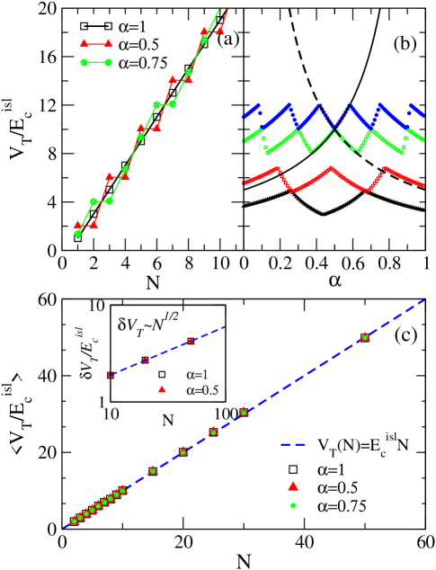
Here for disordered arrays we recover previously predictedMiddleton93 values for the average threshold and its root mean square deviation . is proportional to the number of particles and to . On the contrary, for clean arrays and strictly onsite interactions the threshold voltage differs from the one expected by extrapolating to zero coupling the value obtained for weakly coupled nanoparticles. In particular, for finite coupling (or its zero coupling extrapolation) an -independent threshold voltage is predicted for large arrays, while for strictly zero coupling we obtain . We also show that its value depends on .
The threshold corresponding to the clean case is plotted in Fig. 1(a) for the case of symmetrically biased arrays (), antisymmetrically biased arrays (), and an intermediate biasing (). In the symmetrically biased case, shows a step-like dependence on . There is a clear even-odd effect. The even-odd effect in the threshold voltage with the number of particles is absent for and with a threshold voltage . At strictly zero temperature the tunneling rate and vanishes when is positive or zero. At the inner junctions is independent of the bias voltage and zero or negative if the two islands differ just by just a single charge. Thus the tunneling rate vanishes. junctions prevent the flow of charges. A charge gradient at each bulk junction has to be created to allow flow of charge. In the symmetrically biased case, increasing the potential at the electrodes allows positive and negative charges to enter from the source and the drain respectively. These charges accumulate on the array and create potential drops across the bulk junctions. At voltages just below the threshold, the accumulated charges at the first and last islands are equal in number and opposite in sign. Current starts to flow at voltages larger than when is odd and when is even, as these values allow for the build up of and charges at the first and last islands for odd and even respectively. This corresponds to a charge gradient , across all bulk junctions for odd and across all bulk junctions except one for even . For , charge can only enter the array from one lead and the energy barriers across all bulk junctions must be overcome by accumulated charges. When the first and last junctions are equivalent and charge can enter from both leads so it is possible in some cases for the energy barrier across one of the bulk junctions to be overcome by the potential drop due to two injected charges of opposite sign from the two leads, i.e. one of the junctions can be uncharged. The absence of this possibility is what removes the even-odd effect when and . An intermediate situation is found for .
Complementary information can be obtained by looking at the threshold voltage as a function of for different values of in Fig. 1(b). The threshold voltage changes in a periodic way with . The periods of the features in depend on the number of barriers in the array. Dependence of on and periodic features in with respect to reflect the number of charges which have to accumulate in the first and last island prior to current flow. Fig. 1(b) includes curves corresponding to and for specific values of and . As the assymmetry of the array increases (increasing ), the threshold voltage is alternately determined by the cost of injecting a charge unto the array from the source and the drain. At all except for the values that lead to the minimum for a given array length, the difference in the charge occupying the first and last islands, , equals . At the minimum values of , this charge difference equals .
The clean case of a related system was studied by Hu and O’ConnellHu94 . They analyzed a one-dimensional array of N gated junctions with equal junction capacitances and equal gate capacitances . Due to the finite value of charges in a given island interact with charges in other islands and with charges in the electrodes. With an applied bias voltage the interaction between charges in the electrodes and in the islands results in a bias induced potential drop at the bulk junctions. Once a charge is injected unto the array, it will have no difficulty in traveling through it, and the threshold voltage equals the voltage required for injection of a charge from the electrodes. As the ratio increases the threshold voltage of a long array tends to an N-independent value of the order of the charging energy. The onsite case discussed here corresponds to . If one extrapolates the case discussed by Hu and O’ConnellHu94 to an N-independent threshold voltage would be expected for onsite interactions. As shown above, the threshold voltage of clean arrays does not satifies this prediction, as at zero temperature the charges cannot travel freely through the array, and the threshold voltage increases with the number of islands.
In the case of disordered arrays, each array has a threshold voltage dependent on the given configuration of disorder . The threshold voltage depends on , in a way similar to the clean case. see Fig. 1(b). However, as shown in Fig. 1(c), this dependence on disappears in the average value and we recover Middleton and Wingreen predictionMiddleton93 . For the disordered case Middleton and WingreenMiddleton93 predicted a linear dependence of the threshold voltage on the array length. Upward steps in the disorder potential prevent the flow of charge. The downward steps facilitate it. In average there are upward steps. To overcome such steps a charge gradient has to be created in those junctions. For onsite interactions this results innumeron . In this limit, they also argued that fluctuations in the values of over many random configurations of disorder are analogous to the fluctuations in the net distance traveled by a 1-D random walk with steps, resulting in .
Compared to arrays with no disorder, the threshold of disordered arrays in the onsite limit tends to be smaller because in the clean case, all the bulk junctions inhibit charge flow whereas in the disordered case, only the bulk junctions with positive block charge flow. As shown in the inset of Fig. 1(c), we also recover the relationship for the fluctuations in the threshold predicted by Middleton and WingreenMiddleton93 , .
III FLOW OF CURRENT
For bias voltages larger than threshold the current can flow, but it is a strongly non-linear function of voltage. The current depends on the charging energy and number of islands, the presence or not of charge disorder in the array, the resistances of the junctions and on the asymmetry of the applied bias voltage. Linearity and independence on is recovered at large voltages. As discussed by Middleton and WingreeenMiddleton93 a power-law dependence of the current on voltage is found close to threshold. In this section we discuss the different regimes which can be differentiated in an I-V characteristics and its dependence on the input parameters. At very low voltages by comparing analytical and numerical results we resolve the controversy on the exponent of the power-law and show it to be linear with a slope which depends on and the resistance of the contact junctions, but that is independent on the array length (except in a particular case in which an even-odd effect is found). The linearity is however restricted to very small values of . We also clarify the dependence of the Coulomb staircase profile on the bias parameter and estimate the asymptotic current at high voltages, and the bias voltage at which this high voltage regime is found. Very large values of the bias voltage have to be applied to reach this linear dependence.
III.1 Linear dependence close to threshold
There has been some controversy regarding the power-law of the current with through one dimensional disordered arrays for voltages close to , . Middleton and WingreenMiddleton93 predicted linear behavior for both the long and short range interaction. Reichardt and ReichardtReichhardt03 found a square root behavior using a model with a interaction between the charges in the islands. They argued that is the exponent corresponding to an sliding charge-density wave. They pointed out that the larger values of the exponent obtained by Middleton and WingreenMiddleton93 are a consequence of using voltages which are not small enough. Kaplan et al.Kaplan03 found in the long-range limit of an array of dots capacitively coupled to their nearest neighbors. Finally JhaJha05 and Middleton argued that the dependence of the current of disordered arrays in the onsite limit on for voltages marginally greater than is linear with an slope inversely proportional to the length of the array. Numerically they found an approximate linear behavior only in the case of very long arrays but not for the smallest voltages analyzed (where they found a sublinear dependence) but in an intermediate voltage regime. So far, there are no experiments available in completely one-dimensional arrays, but there are a few in quasi-one dimensional systems. The approximate power-law measuredTinkham99 at voltages is larger than unity which has been attributed to the fact that the system is not strictly one-dimensional.
In this subsection, we show that the current varies linearly with respect to for very small and that the slope is not inversely proportional to . The slope is sensitive to the resistance of the contact junctions and to the degree of symmetry between the applied bias voltages on the source and drain leads. While this linear dependence is found analytically and in the numerical calculations the value of at which it disappears is very small. Because of the small value of the current at such voltages, the linear dependence most probably cannot be seen experimentally.
The linearity above but very close to threshold can be easily understood. Charges can enter only through the contact junctions from the leads. The current through the array is equal to the average charge transferred per unit time. The average time necessary to transfer a charge through the array is the sum of the time involved in all the processes in the sequence of tunneling events from the moment in which charge enters the array from one electrode until it leaves the array to the other one. If the time associated to tunneling at a given junction is much larger than the time involved in the rest of processes, this junction acts as bottleneck and the time necessary to transverse the array is approximately equal to the inverse of the scattering rate through this junction. Thus, the current can be approximated by the tunneling rate across the bottle-neck junction. Below threshold, but close to it, the tunneling at the contact junctions costs finite energy and transport is suppressed. This cost in energy is reduced by the applied bias voltage and at threshold is zero at the entrance junction. When but very close to it, the junction from which the charge enters the array acts as bottle-neck for transport, once it is allowed. At zero temperature, the tunneling rate is . The dependence on bias voltage of the energy for tunneling compared to the one at threshold, at the source and drain junction is, respectively and . If charge enters through a single junction, the current approximately equals
| (7) |
if charge enters from the source, and
| (8) |
if holes enter unto the array from the drain. Both source and drain junctions have to be taken into account in the clean symmetrically biased case when is odd.
| (9) |
When is even and it is necessary that charge enters through both junctions for current to flow and current is approximately equal to
| (10) |
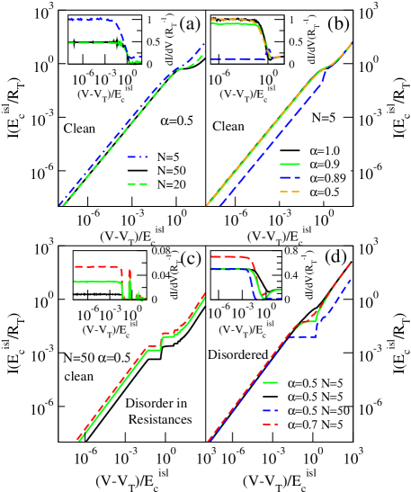
This behavior is observed in Fig. 2. The linear behavior is clearly appreciated in both the log-log scale in which the main figures are plotted as well as in the constancy of the derivatives in the insets. The dependence of the slope of the I-V curves is better seen in the conductance plotted in the insets. As seen in (a) the is equal for the , and curves, i.e. independent on the array length. On the contrary, it is double for . This behavior originates in the even-odd alternancy predicted by Eqs.(9) and (10). The dependence on is studied in Fig.2(b). From top to bottom, the change of slope with is smooth and given by as predicted by (7), but turns non monotonously if currents starts being controlled by (8) with slope . As also expected from the discussion above the slope is affected by disorder in resistances in Fig. 2(c), but not by charge disorder in Fig. 2(d), except in the lose of the even-odd effect present in the clean case for .
III.2 Loss of linear behavior and intermediate regime
The linear behavior in Fig. 2 appears for several orders in magnitude. In spite of this, it disappears for or . The magnitude of the current is probably too small for this linearity to be detected experimentally. We have found that linearity gives rise to sublinear behavior when the time of the other tunneling processes become relevant compared to the time spent at the bottle-neck. Upon increasing the tunneling rates of the different processes involved in the transport become more homogeneous. To obtain sublinear behavior, it is just necessary than the two slowest processes in a sequence have comparable rates. The lost of linearity can depend on the resistance of the junctions when a non bottle-neck junction has a resistance much larger than the bottle-neck one. The bottle-neck character of a process at a junction at the leads can disappear faster for longer arrays as there are more tunneling processes which will contribute to the total time. In the disordered case, the energy gain of some of the tunneling processes is smaller than in the clean case and the contact junctions can stop being the bottle-neck earlier, i.e. for smaller . But, in general we have not found very significative differences for different array parameters in the value of the bias voltage at which the linearity disappears.
As the energy of a tunneling process through an inner junction does not depend on the applied voltage (except via the charge accumulated on it), when a bulk junction controls the transport, the current is independent on voltage showing a characteristic staircase profile. The existence of the Coulomb staircase has been known for a long timesinglecharge ; averinlikharev ; amman91 ; hanna91 . Early claims reported a Coulomb staircase only in the asymmetrically biased casesinglecharge . More recent results in clean capacitively coupled nanoparticle arrays, show that a staircase also emerges in a symmetric array under symmetric biasStopa01 , but claim that the I-V characteristic for an N-dot array under forward bias is identical to that for a 2N-dot one under symmetric bias. We show here that while the appearance of the staircase is generic, the last statement is not correct.
The current has kinks at those voltage values which change the maximum number of charges which can be accumulated at the first or last island, allowing new transport processes. These voltage values depend on the asymmetry and the existence of charge disorder in the array but not on resistance disorder. To allow the addition of an extra charge in the first or last nanoparticle requires an increase in bias voltage in the adjacent electrode of approximately . In the clean case, when only one electrode changes its potential and the width of the steps in bias voltage is . On the other hand, when the change in potential of a given electrode is just the half of the bias voltage and steps appear in intervals of .
With charge disorder and the position of the kinks slightly depends on voltage, but the width of the voltage intervals between the kinks does not change, as new charges are added through a single junction. If , charges enter from both contact junctions but the corresponding kinks in the current do not appear at the same position. While the width of a kink corresponding to a given junction remains in a general case in the I-V characteristic there will be two kinks in each interval in bias voltage due to the alternative position of the kinks of both contact junctions. Except in very special cases the separation of kinks does not do equal .
The position of the kinks in the clean and disorder cases can be observed in Fig. 3. Two main features can be observed. For clean arrays (insets in (a) and (b)) at the onset the current shows a big jump. Once the charge gradient is created and charge can transverse the array, it flows easily. The steps at higher voltages are much smaller but have the width predicted above. In the main figures corresponding to disordered arrays, the large big jump has disappeared and steps are more clearly observed. Two stepwidths, which add are seen for and just steps with width appear for .
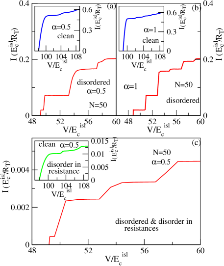
Previously, in the analysis of the threshold voltage, we saw that while the value of has an effect the value for the onset of current, it does not seem possible to determine from a measurement of in the, experimentally relevant case, of a disordered array. However if the onsite interaction case discussed here can be experimentally reproduced, the width of the steps in the I-V curve can differentiate values. Disorder in the resistances does not modify the voltages at which kinks in the current appear but it does affect the staircase profile. The staircase profile is modified in Fig. 2(c), compared to (a) due to the disorder in resistances. A very large resistance in a bulk junction can sharpen the steps, as it creates a bottleneck for the current at a junction with an associated energy for tunneling which does not directly depend on bias voltage, but the opposite behavior can also take place if the large resistance if found at any of the contact junctions. Note that the particular way in which the I-V curve is affected by disorder in resistance depends on the particular resistance and charge-disorder distributions.
III.3 Linear Regime at High-Voltages
At larger voltages linear dependence is recovered. The asymptotic linear I-V does not extrapolate to zero current at zero voltage, but it cuts the zero current axis at a finite offset voltage. This high-voltage linear regime can be understood analytically. We obtain that the slope of the I-V curve depends only on the sum of the junction resistances in series and the offset voltage is given by the sum of the excitonic energies of all the junctions. Contrary to what was found at low voltages, close to threshold, the offset voltage for purely onsite interactions recovers the zero inter-island capacitive coupling valueSchon ; Bakhalov91 calculated starting from a finite value of the inter-island capacitance. To assist comparison with experiments we compute the voltage at which this linear regime is reached.
At very high voltages, the charge gradient ensures that all the tunneling processes to the right decrease the energy. The corresponding tunneling rates are and the total tunneling rate for no resistance disorder is . Having in mind that , . This rate is independent on the selected tunneling process. To transfer a charge from the source to the drain requires in average tunneling events. The average current is thus
| (11) |
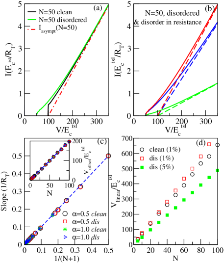
This prediction is compared in Fig. 4 (a) and (c) with numerical results. The slope of the current does not depend on or the existence of charge disorder, but only on the number of junctions . The slope is the same as obtained adding all the resistances in series. Asymptotically, at low voltage, this curve cuts the axis at the offset voltage . This value is, in general, different to the threshold voltage and independent of the resistance of the junction and the asymmetry of the bias voltage.
Previous derivation is valid even if there is inhomogeneity in the value of island capacitances but relies on the homogeneity of the junction resistances through the array. If this is not the case the total tunneling rate of each step in a sequence is . One could argue that on average, the charge gradient would be such that it ensures a uniform tunneling rate through all the junctions. The potential drop which gives such a tunneling rate is and with . There are possible tunneling events at each step in a sequence and steps, thus both factors cancel our. The resulting average current is
| (12) |
As in the uniform resistance case, the slope in the current corresponds to the addition in series of all the resistances. The predicted asymptotic high-voltage behavior is observed in Fig. 4 for arrays with different parameters. Note that as longer is the array larger voltages have to be applied to reach this voltage. The voltage at which the linear behavior is reached is estimated in Fig. 4(d). It is approximately three times the offset voltage and slightly larger in the presence of charge disorder. In long arrays can become very large and the linear behavior will not be easily reached experimentally.
IV Potential drop through the array
The potential through the array can nowadays be measuredSample02 , but to our knowledge it has not been studied theoretically. In conventional ohmic systems with a linear current-voltage relation the potential drops homogeneously through the array if the resistivity of the system is homogeneous. When the proportionality constant between voltage and current is given by the sum of the resistances in series, but these resistances are not all equal, the voltage drop at each point is proportional to the local resistance. The nanoparticle array I-V characteristics are highly non-linear and in general it is not obvious how the potential drops through it. At the islands the potential is the sum of the disorder and charge terms, while at the electrodes the potential is controlled by the applied bias. As seen above, there are two linear regimes which can be identified. At high voltages the differential conductance equals the inverse of the sum of the resistances in series. Naively, a potential drop proportional to the resistance at each junction could be expected at these voltages, but we will see that this is not exactly the case. In the low-voltage regime the slope of the current does not correspond to the addition of the resistances in series, but it is proportional to a single one (to the sum of two of them in the symmetric case) and it is not clear that the potential drop should be proportional to the junction resistance. In this section we study the potential drop through the array at low, intermediate and high voltages and show that in none of these regimes the potential drop at a given junction is strictly proportional to its resistance. In the linear regimes we show that deviations from this proportionality are related to the offset voltages and filling of the array. In the intermediate regime the voltage drop oscillates with position and reflects correlations between the charges.
IV.1 High-Voltage Regime
We start with the high-voltage linear regime, as it is the easiest to understand. Fig. 5 shows the average potential drop in a clean and a disordered array for a given bias voltage in the high-voltage linear regime. All the junction resistances are equal in the top figures. The average voltage drop is equal in both the clean and disordered case, and at first sight it seems linear. A linear potential drop through the array implies a homogeneous average junction potential drop. However, at the contact junctions is approximately times smaller than at the bulk junctions. The voltage drop at each junction is not equal to the current divided by the junction resistance either, as could be naively expected. The reasons for these deviations can be found in the offset voltage in the I-V curve and in Eq. (3) which gives the change in energy for tunneling.
At high voltages the I-V curve is linear but the total voltage drop through the array does not equal . As, seen in equation (12), there is an offset voltage . This offset voltage reflects the excitonic energy cost for tunneling. The excitonic energy is not equal at each junction. It is at the bulk junctions and approximately at the contact ones. Only the extra potential drop at each junction gives a finite contribution to current through it. On average
| (13) |
From current conservation at high voltages the average potential drop through the array
| (14) |
It is not affected by the presence of charge disorder in the array (but it would change if capacitances are not homogeneous, via ). As observed in Fig. 5, Eq (14) gives a good estimate of the potential drop. The validity of Eq(14) is better seen when is plotted. It is proportional to the resistance of the junction and equal in every junction if all resistances are the same. This statement is valid independently on the position of the resistance, as shown in the bottom figure of Fig. 5 and its inset and on the asymmetry of the applied voltage (not shown). The dependence of on the junction resistance is easily understood. The tunneling probability through a junction depends on its resistance. It is inversely proportional to it. When the resistance is very large, the charge has a lesser tendency to jump from an island to its neighbor and it will spend more time in the island producing a dependence of the time-averaged potential drop on the junction resistance distribution.
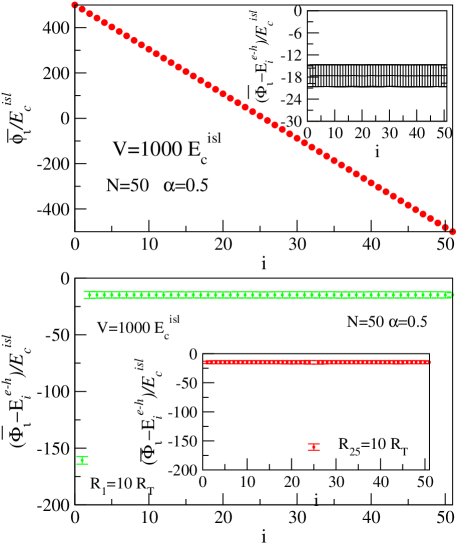
As seen above, in this high-voltage linear regime the current can be obtained from the average tunneling rate and correspondingly from the average potential drop. Deviations of the average value , i.e. the root mean square (r.m.s.), are shown in the inset in Fig.5, in the form of error bars. They are slightly smaller at the contact junctions as the potential at the electrodes is restored to its nominal value via a battery prior to any tunneling event and larger at junctions with a larger resistance. Fluctuations in the local voltage drop increase with applied bias voltage as the number of possible charge states and the width of the distribution of hopping energies do. Fluctuations are larger at those junctions with a larger resistance, but is smaller.
IV.2 Low-voltage regime
Close to threshold the current depends linearly on . Here we show that in this linear regime the average potential drop mainly reflects the charge state of the array at threshold. This charge state depends on the asymmetry of the voltage drop and disorder and in a symmetrically biased clean array on the even or odd number of islands. For , charges enter from the source and bulk junctions prevent charge motion. If an electron reaches the last nanoparticle, it can freely jump onto the drain at zero potential. There is no charge gradient at the drain junction. Consequently, the potential drop at this junction vanishes at threshold. On the contrary, at the bulk junctions there is a charge gradient equal to unity, with the corresponding potential drop . To allow current equals the excitonic energy of the first junction, approximately equal to . Close to threshold, as the bottle-neck for the current is the entrance of electrons from the source the charge state of the array is most of the time equal to the one at threshold, and only perturbed by the fast passage of charges. The average potential drop, plotted in Fig. 6(a) for a clean array with all junction resistances equal is almost the same as the static potential drop at threshold.
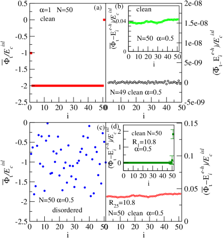
For and odd number of particles, at threshold the charge gradient and charge potential drop in a clean array are respectively one and at the bulk junctions. At the contact junctions the potential drop is . As in the case discussed above, the average potential drop in the linear regime close to threshold, is very close to the one found at threshold, which equals the excitonic energy at each junction, , what can be seen in the main figure in Fig. 6(b). When the number of particles is even, the charge gradient at one of the junctions vanishes. As shown in the inset of Fig. 6(b), in the bottleneck regime is positive and equal for all the junctions. This reflects that every junction is uncharged with equal probability.
In the disordered case, only those junctions with upward steps in the disorder potential are charged, and this is reflected in the average potential drop, in Fig.6 which adds disorder, charge and bias potential.
The threshold voltage does not depend on the resistance of the junctions, but the flow of charge does. This is reflected on the average potential drop on such very small scale that even if the threshold voltage potential drop is substracted at each junction and for reasonably large changes in resistance it is not visible (see main figure in Fig. 6(d). This is different to the dependence observed in the high-voltage regime. For extremely large values of the resistance disorder a weak effect on the average voltage at bias close to threshold can be seen (not shown). In this case, the potential drop at a junction with a larger resistance is slighltly larger than at the rest. At the adjacent junctions it is slightly smaller, what reflects the average charge state of the nanoparticles joined by the large resistance.
The r.m.s of the junction potential drop at low bias voltages are very small in some of the cases analyzed, of order in main figures in Fig. 6(a) and (b). Error bars are small because most of the time the array is at the threshold charge state. This is not the case in the inset in 6(b) where fluctuations are or the order of , or in the inset in 6(d) where they are small everywhere except at the last two junctions where they are of order . Disorder also increases the fluctuations in the average voltages to values of the order of the charging energy.
IV.3 Intermediate Voltage Regime
The most interesting regime to analyze the voltage drop is at intermediate voltages where the I-V curve show the Coulomb staircase. For the case of a clean array with capacitively coupled nanoparticles StopaStopa01 showed that the steps in the I-V characteristic correspond to alternation of the charge density between distinct Wigner crystalline phases. In our case, the interaction is short-range, but the possibility of such a Wigner state with charges periodically ordered to minimize their repulsion, if present, could be observed via the potential drop. Periodic charge ordering should lead to oscillations in the potential drop along the array. Such an observation would be a clear evidence of correlated motion.
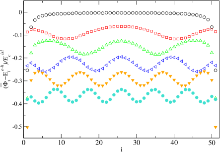
The average potential drop (with the excitonic energy subtracted) through the array for several voltages corresponding to clean N=50 nanoparticle arrays is shown in Fig. 7. Clear oscillations are seen. Comparing the values of the bias voltage chosen with the position of the steps in the corresponding I-V curve in Fig. 7, the number of maxima/minima in the potential drop do not change in a given step in the Coulomb staircase. For symmetrically biased arrays, they increase in pairs from a step to the next one. For odd/even number of particles, there is always a minimum/maximum at the center of the array. The other maxima and minima tend to be as equally spaced as possible, but this is not exact. Inconmensurability beween the period of the oscillations and the lattice can distort equal spacement. Also, when new maxima or minima appear they are closer to the source and drain electrodes and move inwards, producing a movement of the other maxima and minima, with increasing voltage. This can be taken as a finite size effect of the Wigner crystal state. As the number of charges in the array increase with increasing bias voltage the amplitude and period of the oscillations decreases, approaching the high-voltage regime for which is homogeneous.
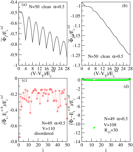
The anomalous potential drop can be also seen in the potential drop at a given junction as a function of the bias voltage, shown in Fig 8(a) and 8(b) for junctions 1 and 25 for a clean symmetrically biased 50-islands array At the first junction the potential drop show clear oscillations as a function of the bias voltage, which reflect that new charges state at the first island are allowed. The potential drop increases until an extra charge can be accumulated at the first nanoparticle, for larger voltages the average occupation of first island increases and the voltage decreases smoothly until a new value at which it increases again as the increase in occupation of first island cannot compensate the increase in the electrode potential. Oscillations, but less regular and less pronounced due to the movement of maxima and minima discussed above, are also observed at intermediate junctions . Potential drop is much more homogeneous at the middle of the array, where there is always a minimum (or maximum) in the potential drop.
Charge or resistance disorder alters the charge motion and frustrates the formation of this Wigner crystal like state, as seen in Fig. 8(c) and 8(d). This is the opposite behavior that would be naively expected if one just associates the appearance of plateaux with the oscillations in voltage drop and emphasizes that the step profile is just a consequence of the dependence on the bias voltage of the tunneling rate of the processes which control the current.
The r.m.s. of the junction potential drop is larger than at low voltages and smaller than at high voltages. It is of the order of the excitonic energy and reflects the variation in occupation of the island. It slowly increases with voltage.
V Summary
In this paper we have studied, analytical and numerically, the current through an array of metallic islands placed in between two large electrodes, the source and the drain at voltages and respectively. The applied bias voltage satisfies . Interactions are restricted to those charges in the same conductor. The capacitive coupling between different conductors vanishes. The nanoparticle level spacing is assumed negligible and transport is treated at the sequential tunneling level. In the model used we take into account that the electrodes are not ideal voltage sources, but have a finite self-capacitance. This means that the voltage at the electrodes fluctuates in response to tunneling processes, but we assume that prior to the next tunneling event the nominal voltage is restored. Due to the large value of the electrode capacitance numerical results are barely modified and its effect is neglected in the discussion. The probability of each process depends on the change in energy involved, which can be written as the energy to create an electron-hole pair plus the difference in potential between the sites involved in the tunneling, see Eq.(3). We have analyzed and clarified how the transport properties depend on the number of particles, the presence of charge or resistance disorder and the bias voltage, including how symmetrically it is applied. To quantify this symmetry we have introduced a parameter as .
We have shown that in the purely onsite interaction limit the dependence of the threshold voltage of clean arrays on the number of nanoparticles differs qualitatively of the dependence predicted for weakly coupled islands, as in the onsite case studied here a charge cannot flow freely through an empty array. For symmetrically biased arrays equals for odd and for even . The even-odd effect disappears for forward biasing () and , see Fig. 1(a). The threshold voltage is not affected by disorder in the junction resistances but it depends on the selected disorder configuration if charge disorder is present. With charge disorder, the average threshold voltage is independent on and we recover previously predicted values , see Fig. 1(b).
At voltages marginally close to threshold, current is linear on with a slope independent on the number of particles but which depends on the resistance of the contact junctions and on the bias asymmetry , see Eqs. (7) to (9) and Fig. 2. This dependence has been obtained both numerical and analytically and resolves previous controversy on the power-law close to threshold. It reflects that the junction through which charges enter into the array acts as a bottle neck. The range of voltages at which this linear dependence holds is probably too small to be observed experimentally. Linearity is lost when the scattering rate for tunneling through the contact junctions is comparable to other tunneling processes scattering rates.
The linear regime is followed by a Coulomb staircase at intermediate voltages. The width of the steps depends on and on the presence of charge disorder. For clean arrays the bias voltage step width is for forward bias and for symmetric bias. The stepwidth changes if disorder is present but still depends on the value of . The staircase profile depends on the junction resistances values. See Fig. 3.
At high voltages current depends linearly on bias voltage. The asymptotic I-V characteristic is given by (12) and cuts the zero current axis at a finite offset voltage, see Fig. 4. The slope of the asymptotic linear I-V is given by the inverse of the sum of the junction resistances in series and the offset voltage takes into account charging effects. The high-voltage linear behavior is reached for bias voltages approximately three times larger than the offset. can be very large long arrays.
We have studied the potential drop through the array and showed that in none of the transport regimes studied it drops completely linearly through the array. In the low-voltage linear regime the average potential drop mainly reflects the charge gradient created at threshold, see Fig. 6. The effect of disorder in resistances is extremely weak, except for symmetrically biased arrays with even number of particles. In the Coulomb staircase regime the potential drop along the array show almost periodic oscillations in disorder-free arrays which reflect the correlated motion and the tendency to form a Wigner-crystal like state, see Fig. 7. Such periodicity is destroyed by charge or resistance disorder in Fig. 8. In the high-voltage regime the ohmic dependence, and the associated proportionality between the potential drop and the junction resistance , is only recovered once the excitonic energy is substracted, as seen in (14) and Fig. 5. The mean value of the potential drop serves to compute the I-V characteristic in this regime.
VI Appendix: Simulation
We numerically determine the time evolution of the state of an array of nanoparticles sandwiched between two large metallic leads symmetrically biased at potentials and , with . The state of the array consists of the set of charges that occupy the array islands and the leads. The island charges take on integer values. The charge of the nanoparticles is modified when an electron tunnels between two adjacent sites. The charges of the source and drain can take on any real value because they can be modified discretely via the tunneling of charges or continuously via the charging of the leads by a battery.
The evolution of the system is computed by means of a kinetic Monte Carlo simulationBakhalov89 . At each iteration a single tunneling event takes place. The time involved in this event depends on the tunneling rates of all the possible tunneling processes. Each iteration starts from an initial charge configuration. First, it is computed the change in energy and the tunneling rate of the possible hopping events, corresponding to the tunneling of a single electron, to the left or to the right, through any of the junctions. The probability of changing the initial configuration varies with time like
| (15) |
with the time at which the preceding tunneling process took place and . and are the tunneling rates through the junction to the left or to the right, respectively, and are calculated from (1). To sample the time interval between two hopping events we generate random numbers between to mimic and obtain from (15). As the average of is the unity, if one is interested only in the average values of the charge or the current, and not on its fluctuations, the time step could be fixedEfros03 to . This option is numerically faster.
The relative probability of each tunneling event is . To determine the hopping process which changes the charge state, the relative probabilities are consecutively arranged in the interval . A second random number in this interval is generated to select the tunneling process.
Then, the charge configuration is updated. After we modify the state of the system, we allow the external circuit to return the leads to their applied bias values prior to the selection of the next hop. This effect is simulated by resetting the charges on the source and the drain to the values that restore the nominal applied bias.
In order to remove all sensitivity to initial conditions, before we track the evolution of as a function of time at any voltage, we perform iterations to equilibrate the system. Following these iterations, we track the evolution of the charge state until the net number of electrons that arrive at the drain, , equals a very large number (). The average calculated current is given by
| (16) |
where is the sum of all time intervals between hopping processes in the evolution runs. If a tunneling event involving the drain is selected, an amount is added to depending on whether an electron hopped to or from the drain. Current conservation ensures that the average current is the same through any junction. The minimum numbers of equilibration cycles, , and evolution cycles (set by ) depend on the voltage.
To calculate the average voltage drop, we assume that the system is in a given state a time equal to the interval until the next tunneling event takes place.
Financial support from the Swiss National Foundation, NCCR MaNEP of the Swiss National Fonds, the Spanish Science and Education Ministry through Ramón y Cajal contract and FIS2005-05478-C02-01 grant and the Dirección General de Universidades e Investigación de la Consejería de Educación de la Comunidad de Madrid and CSIC through grant 200550M136 is gratefully acknowledged. Work at UT Austin was supported by the Welch Foundation by the NSF under grant DMR-0606489 and by the ARO under grant W911NF-07-1-0439.
References
- (1) R.L.Whetten, J.T. Khoury, M.M. Alvarez, S.Murthy, I. Vezmar, Z.L. Wang, P.W. Stephens, C.L. Cleveland, W.D. Luedtke and U. Landman, Adv. Mater. 8, 428 (1996).
- (2) C.P. Collier, R.J. Saykally, J.J. Shiang, S.E. Henrichs, J.R. Heath, Science 277, 1978 (1997). G. Markovich, C. P. Collier, S.E. Henrichs, F. Remacle, R.D. Levine and J.R. Heath, Acc. Chem. Res. 32, 415 (1999).
- (3) R. Parthasarathy, X-M Lin and H. M. Jaeger, Phys. Rev. Lett. 87, 186807 (2001)
- (4) J.D. Le, Y. Pinto, N.C. Seeman, K. Musier-Forsyth, T.A. Taton and R.A. Kiehl, Nanoletters 4, 2343 (2004).
- (5) Y. Lin, A. Böker, J. He, K. Sill, H. Xiang, C. Abetz, X. Li, J. Wang, T. Emrick, S. Long, Q. Wang, A. Balazs and T.P. Russell, Nature 434, 55 (2005).
- (6) K. Elteto, X.-M. Lin and H.M. Jaeger, Phys. Rev. B 71, 205412 (2005).
- (7) J. Zhang, Y.Liu, Y. Ke and H. Yan, Nanoletters 6, 248 (2006).
- (8) T.P. Bigioni, X.-M.Lin, T.T. Nguyen, E.I. Corwin, T.A. Witten and H. M. Jaeger, Nature Materials 5, 265 (2006).
- (9) J. Liao, L. Bernard, M. Langer, C. Schönenberger and M. Calame, Adv. Mater.18, 2803 (2006). (ojo comprobar si es 2803 o 2444).
- (10) S.S. Mark, M. Bergkvist, X. Yang, L.M. Teixeira, P. Bhatnagar, E. R. Angert and C.A. Batt, Langmuir 22, 3763 (2006).
- (11) C.B. Murray, C.R. Kagan and M.G. Bawendi, Science 270, 1335 (1995).
- (12) D.V.Talapin, E.V. Shevchenko, A. Kornowski, N. Gaponik, M. Haase, A.L. Rogach and H. Weller, Adv. Mater. 13, 1868 (2001).
- (13) N.Y. Morgan, C.A. Leatherdale, M. Drndíc, M.V. jarosz, M.A. Kastner and M. Bawendi, Phys. Rev. B66, 075339 (2002). V.J. Porter, t. Mentzel, S. Charpentier, M.A. Kastner and M.G. Bawendi, Phys. Rev. B 73, 155303 (2006).
- (14) D. Yu, c. Wang, B.L. Wehrenberg and P. Guyot-Sionnest, Phys. Rev. Lett. 92, 216802 (2004).
- (15) H. Romero and M. Drndic, Phys. Rev. Lett. 95, 156801 (2005).
- (16) T. Feng, H. Yu, M. Dicken, J.R. Heath and H.A. Atwater, App. Phys. Lett. 86, 033103 (2005).
- (17) S. Sun, C.B. Murray, D. Weller, L. Folks and A. Moser, Science 287, 1989 (2000).
- (18) C.T. Black, C.B. Murray, R.L. Sandstrom and S. Sun, Science 290, 1131 (2000)
- (19) V. F. Puntes, P. Gorostiza, D.M. Aruguete, N.G. Bastus and A.P. Alivisatos, Nature Materials 3, 263 (2004).
- (20) F.X. Redl, K.-S. Cho, C.B. Murray and S. O’Brien, Nature (London) 423, 968 (2003).
- (21) A.E. Saunders and B. A. Korgel, Chem. Phys. Chem. 6, 61 (2005).
- (22) E.V. Schevchenko, C.V. Talapin, N.A. Kotov, S. O’Brien and C.B. Murray, Nature (London) 439, 55 (2006).
- (23) Single Charge Tunneling, NATO ASI Series, Vol B, 294, eds. H. Grabert and M.H. Devoret., New York, Plenum Press 1992.
- (24) P. Sheng and B. Abeles, Phys. Rev. Lett. 28, 34 (1972). P. Sheng, B. Abeles and Y. Arie, Phys. Rev. Lett. 31, 44 (1973). J.S. Helman and B. Abeles, Phys. Rev. Lett. 37, 1429 (1976).
- (25) J.J. Shiang, J.R. Heath, c.P. Collier and R.J. Saykally, J. Phys. Chem. B 102, 3425 (1998).
- (26) S.-H. Kim, G. Medeiros-Ribeiro, D.A.A. Ohlberg, R.S. Williams and J.R. Heath, J. Phys. Chem. B 103, 10341 (1999). J.F. Sampaio, K.C. Beverly and J.R. Heath, J. Phys. Chem. B, 105, 8797 (2001)
- (27) I.S. Weitz, J.L. Sample, R.Ries, E.M. Spain and J.R. Heath, J. Phys. Chem B 104, 4288 (2000).
- (28) B.M. Quinn, I. Prieto, S. K. Haram and A.J. Bard, J. Phys. Chem. B 105, 7474 (2001).
- (29) R.C. Doty, H. Yu, C.K. Shih and B.A. Korgel, J. Phys. Chem. B 105, 8291 (2001).
- (30) A. Courty, A. Mermet, P.A. Albouy, E. Duval and M.P. Pileni, Nature Materials 4, 395 (2005).
- (31) A.A. Middleton and N.S. Wingreen, Phys. Rev. Lett. 71, 3198 (1993).
- (32) K.A. Matsuoka and K.K. Likharev, Phys. Rev. B 57, 15613 (1998). D.M. Kaplan, V.A. Sverdlov and K.K. Likharev, cond-mat/0303477.
- (33) M.Shin, S. Lee, K.W. Park and E.H. Lee, Phys. Rev. Lett. 80, 5774 (1998).
- (34) D.M. Kaplan, V.A. Sverdlov and K.K. Likharev, Phys. Rev. B 65, 193309 (2002).
- (35) D.A. Kaplan, V.A. Sverdlov and K.K. Likharev, Phys. Rev. B 68, 045321 (2003).
- (36) Y.A. Kinkhabwala, V.A. Sverdlov, K.K. Likharev, J, of Phys. Condens. Matter 18 2013 (2006).
- (37) R.Kotliar and S. Das Sarma, Superlatt. and Microst. 20, 641 (1996).
- (38) I.S. Beloborodov, A.V. Lopatin, V.M. Vinokur and K.B. Efetov, Rev. Mod. Phys. 79, 469 (2007). I.S. Beloborodov, A. Glatz and V.M. Vinokur, Phys. Rev. B 75, 052302 (2007). T.B. Tran, I.S. Beloborodov, X.M. Lin, T.P. Bigioni, V.M. Vinokur and H.M. Jaeger, Phys. Rev. Lett. 95, 076806 (2005).
- (39) A. Atland, L. Glazman, A. Kamenev, Phys. Rev. Lett. 92, 026801 (2004). J.S. Meyer, A. Kamenev and L.I. Glazman, Phys. Rev. B 70, 045310 (2004).
- (40) Y.L. Loh, V. Tripathi and M. Turlakov, Phys. Rev. B 72, 233404 (2005).
- (41) K.B. Efetov and A. Tschersich, Europhys. Lett. 59, 114 (2002).
- (42) J. Zhang and B.I. Shklovskii, Phys. Rev. B 70, 115317 (2004).
- (43) R. Parthasarathy, X.-M. Lin, K. Elteto, T.F. Rosenbaum and H.M. Jaeger, Phys. Rev. Lett. 92, 076801 (2004). K. Elteto, E. G. Antonyan, T. T. Nguyen, and H. M. Jaeger, Phys. Rev. B 71, 064206 (2005).
- (44) K.C. Beverly, J.F. Sampaio and J.R. Heath, J. Phys. Chem B 106, 2131 (2002). F. Remacle, C.P. Collier, G. Markovich, J.R. Heath, U. Banin, R.D. Levine J. Phys. Chem B 102, 7727 (1998). F. Remacle, K.C. Beverly, J.R. Heath and R.D. Levine, J. Phys. Chem B 106 4116 (2002).
- (45) A.S. Cordan, A. Goltzené, Y. Hervé, M. Mejías, C. Vieu and H. Launois, Jour. of App. Phys. 84, 3756 (1998). A. Pépin, C. Vieu, M. Mejias, Y. Jin, F. Carcenac, J. Gieraz, C. David, L. Couraud, A. S. Cordan, Y. Leroy and A. Goltzené, App. Phys. Lett. 74, 3047 (1999). A.S. Cordan, Y. Leroy, A. Goltzené, A. Pepin, C. Vieu, M. Mejias and H. Launois, Jour. of App. Phys. 87 345 (2000). Y. Leroy, A. S. Cordan and A. Goltzené, Jour. of App. Phys. 90 953 (2001).
- (46) N.S. Bakhalov, G.S. Kazacha, K.K. Likharev and S.I. Serdyukova, Sov. Phys. JETP 68, 581 (1989).
- (47) S. Semrau, H. Schoeller and W. Wenzel, Phys. Rev. B 72, 205443 (2005).
- (48) M.G. Ancona, W. Kruppa, R.W. Rendell, A.W. Snow, D. Park and J.B. Boos, Phys. Rev. B 64, 033408 (2001).
- (49) A. Bezryadin, R.M. Westervelt, and M. Tinkham, App. Phys. Lett. 74, 2699 (1999).
- (50) G.Y. Hu and R.F. O’Connell, Phys. Rev. B 49, 16773 (1994).
- (51) J.A. Melsen, U. Hanke, H.O. Müller and K.A. Chao, Phys. Rev. B 55, 10638 (1997).
- (52) C.A. Berven and M.N. Wybourne, App. Phys. Lett. 78, 3893 (2001).
- (53) C. Kurdak, A.J. rimberg, T.R. Ho and J. Clarke, Phys. Rev. B 57, R6842 (1998).
- (54) S. Jha and A.A. Middleton, cond-mat/0511094
- (55) C.Reichhardt and C.J. O. Reichhardt, Phys. Rev. Lett. 90, 046802 (2003).
- (56) E. Bascones,J.A. Trinidad, V. Estévez and A.H. MacDonald, cond-mat
- (57) Some previous work on capacitance disorder can be found inMelsen97 ; Jha05
- (58) Y. Xue and M.A. Ratner, Phys. Rev. B 68, 235410 (2003).
- (59) M. Stopa Phys. Rev. B 64, 193315 (2001).
- (60) D.V. Averin and K.K. Likharev, Mesoscopic Phenomana in Solids, edited by B.L. Altshuler, P. A. Lee, and R.A. Webb (Elsevier, Amsterdam, 1991).
- (61) M. Amman, R. Wilkins, E. Ben-Jacob, P.D. Maker, and R.C. Jaklevic, Phys. Rev. B 43, 1146 (1991).
- (62) A.E. Hanna and M. Tinkham, Phys. Rev. B 44, 5919 (1991).
- (63) U. Geigenmüller and G. Schön, Europhys. Lett. 10, 765 (1989).
- (64) N.S. Bakhalov, G.S. Kazacha, K.K. Likharev and S.I. Serdyukova, Physica B 173, 319 (1991).
- (65) J.L. Sample, K.C. Beverly, P.R. Chaudhari, F. Remacle, J.R. Heath and R.D. Levine, Adv. Mater. 14 124 (2002).
- (66) InMiddleton93 the average threshold voltage is predicted to be linear on the number of junctions, which in our case is . It is straightforward to argue for both that is linear in the number of bulk islands as observed in Fig.1(b). In large arrays the difference between both predictions is negligible.
- (67) D.N. Tsigankov, E. Pazy, B.D. Laikhtman and A.L. Efros, Phys. Rev. B 68, 184205 (2003)